


1. Introduction
According to the prediction of Cahners In-stat Group, a market research company, in the next few years, the image products based on CMOS image sensors will reach more than 50%, that is to say, CMOS image sensors will replace CCD and become the mainstream of the market. It can be seen that the market prospect of CMOS cameras is very broad [1]. CMOS image sensors (CIS) have become an important component in the technology sector, with applications in various electronic devices such as cellphones, cameras, surveillance systems, space, and medical equipment among others [2]. They can take different forms, including line-scan, area-scan, and depth image scanners, for various imaging modalities such as visible light, infrared (NIR and LWIR), X-ray imaging, and more.
CIS is used in the automotive industry as well as in industrial and consumer markets. In medical and scientific areas, CIS is used for a variety of applications as well. Specifically, low noise, high dynamic range, and speed are key features of interest in the industrial and scientific fields. The versatility of CIS allows them to be utilized in different industries. For instance, in the automotive field, they are used in advanced driver assistance systems (ADAS) for collision avoidance, lane departure warnings, and more. In the industrial field, they are used for quality control inspection and monitoring processes.
In the scientific area, CIS help to capture and analyze images for research and experimentation. Medical applications of CIS include endoscopy and microscopy, among other things. Overall, the ability of CIS to function across multiple industries and different imaging modalities has made them an indispensable tool in the field of modern technology
The principle of CMOS image sensor was put forward in the late 1960s, but it was put into practical use after the development of semiconductor micro-machining technology in the 1990s [1]. Before that, the Charge-coupled Device(CCD) is in the dominant place of the image sensor area. Along with the improvement of microelectronics technology, especially in recent years, the development of micro and nanotechnology is represented by the microelectromechanical systems (MEMS) and micro optoelectromechanical systems (MOEMS). They all provide fundamental production equipment for CMOS image sensors because they can fit the existing CMOS semiconductor manufacturing process, and at the same time meet the image quality requirements of the CCD image sensors which need a dedicated production line. As the demands for image sensor increase, CCD is difficult to meet the requirements in terms of volume, weight, and power consumption. On the contrary, the CMOS image sensor has the characteristics of low power consumption, small size, and small weight, which makes it possible to realize the image acquisition function [3].
In 1963 [1], Morrison published a programmable sensor, with a structure that can measure the position of light spots by using the photoconductive effect, and became the beginning of the development of the CMOS image sensor.
The CMOS image sensor is a solid-state imaging sensor that shares a common historical origin with CCD. Typically, the CMOS image sensor consists of an array of image-sensitive units, row drivers, column drivers, timing control logic, analog-to-digital (AD) converters, data bus output interfaces, and control interfaces. These components are usually integrated onto the same silicon chip.
The purpose of the review paper is to introduce the function of the CMOS image sensor, analyze the structure and components of image sensors, and explain its working principle. Explain the advantages and disadvantages of the CMOS image sensor compared with other sensors. Summarize the application of CMOS image sensor in different fields, and focus on the application of monitoring, aerospace, and medical fields. Analyze the special needs of various fields and the characteristics of CMOS image sensors to meet these needs.
2. CMOS image sensors
An image sensor is an electronic device that converts incident photons of light into corresponding electrical signals [4]. The image sensor typically consists of three main components: the pixel array, readout circuits, and driver circuits [5]. The architecture of a CMOS image sensor is illustrated below.
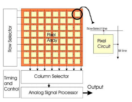
Figure 1. CMOS image sensor architecture [5].
Conventional image sensors employ various technologies, including photodiodes, photogates, and charge-coupled devices (CCD), among others. Photodiodes are utilized to convert incoming light into electrical signals or electrons. The photodiode absorbs incident photons, generating a flow of electrons. However, to collect these electrons, the photodiode must operate at high voltages.
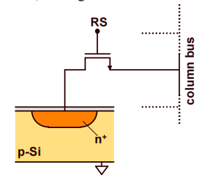 In modern times, the photodiode pixel is commonly utilized in CMOS image sensors. The pixel's structure is uncomplicated, consisting of solely a photodiode paired with an addressing transistor switch. There are two types of pixel structures, which is passive pixel sensors(PPS) that were developed earlier and active pixel sensor(APS) developed later in order to improve the quality of an image. APS is named after the introduction of an active amplifier in the circuit, where the amplifier can improve the performance of the pixel. The first structures are used in CMOS image sensors are Passive Pixel Sensors(PPS). As shown in Figure 2.
Figure 2. Passive CMOS pixel based on a single in-pixel transistor [6].
Passive pixel circuits are composed of photodiodes without any amplification within the structure. These pixel structures are composed of photodiodes and transistors, which are interconnected to the readout structure. After pixel addressing is accomplished by activating the selection line transistor, the pixel is reset via the bit line and selection line transistor.
Passive pixels operate according to the following principle: when an exposure commences, a high voltage is applied in reverse to the photodiode [6]. When photons enter during the exposure phase, they cause a decrease in the reverse voltage across the photodiode. At the end of the exposure time, the remaining voltage across the diode is measured, and the difference from the initial value indicates the number of photons that impinged on the photodiode during exposure. To prepare for a new exposure cycle, the photodiode is reset.
Nonetheless, passive pixel circuits experience elevated levels of noise and reduced sensitivity due to the significant capacitance of the column, which leads to a mismatch between the small capacitance of the pixels and the large capacitance of the vertical bus. This limitation has led to the development of alternative designs, such as the active pixel sensor (APS), which includes an amplifier in each pixel to improve sensitivity and reduce noise levels. Despite these drawbacks, passive pixel circuits remain prevalent in applications such as digital cameras and image scanners. However, the significant capacitance of the column results in high levels of noise and reduced sensitivity, which stems from the mismatch between the small capacitance of the pixel and the large capacitance of the vertical bus.
To address the issue of noise performance, the active pixel concept was introduced, resulting in the creation of active pixel sensors (APS). Each pixel in an APS is equipped with its own in-pixel amplifier. As shown in Figure 3.
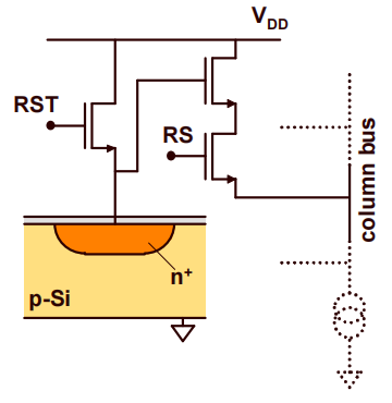
Figure 3. Active CMOS pixel based on an in-pixel amplifier [6].
The active pixel sensor (APS) improves upon the limitations of passive pixel circuits by integrating an amplifier in each pixel to improve sensitivity and reduce noise levels. The amplifier is a source follower that is inactive during the readout state. The working principle of APS is similar to that of passive pixel sensors. The process starts with the reverse biasing or resetting of the photodiode. During the exposure phase, photons that strike the photodiode cause a decrease in the reverse voltage across it. After the exposure period ends, the pixel is addressed, and the voltage across the diode is transferred outside of the pixel using the source follower. To prepare for a new exposure cycle, the photodiode is reset once more.
Yet, APS also has some disadvantages, notably elevated fixed pattern noise, which stems from variations in the transistor's threshold level and gain resulting from alterations to the wafer process. To mitigate this noise, a sampling circuit known as a correlation double sampling (CDS) circuit can be implemented. The CDS circuit minimizes video background shifts that occur due to changes in the threshold level.
Overall, APS represents a significant improvement over passive pixel sensors, offering higher sensitivity and lower noise levels. With the addition of a CDS circuit, APS can further improve its performance, making it the preferred technology for many imaging applications. The CMOS image sensor adopts the standard CMOS semiconductor production process, which inherits the advantages of CMOS technology, such as extremely low static power consumption, dynamic power consumption proportional to the working frequency, large noise tolerance, strong anti-interference ability, especially suitable for working under harsh noise environment, fast working speed, and only need a single power supply. The advantages of CMOS image sensor compared with CCD make the former develop rapidly and widely used in industrial technology and civil video technology. Although it still has some problems, such as slightly higher dark current, high resolution, and high-performance devices, which need further development, I believe these problems can be solved.
3. Application
To ascertain the primary uses of CMOS image sensors, an exhaustive review of the literature was conducted, with a focus on their applications in diverse fields including, but not limited to, automotive, Internet of Things (IoT), medical, intelligent surveillance systems (ISS), space, military, and wireless sensor networks (WSNs) [5]. As shown in Figure 4.
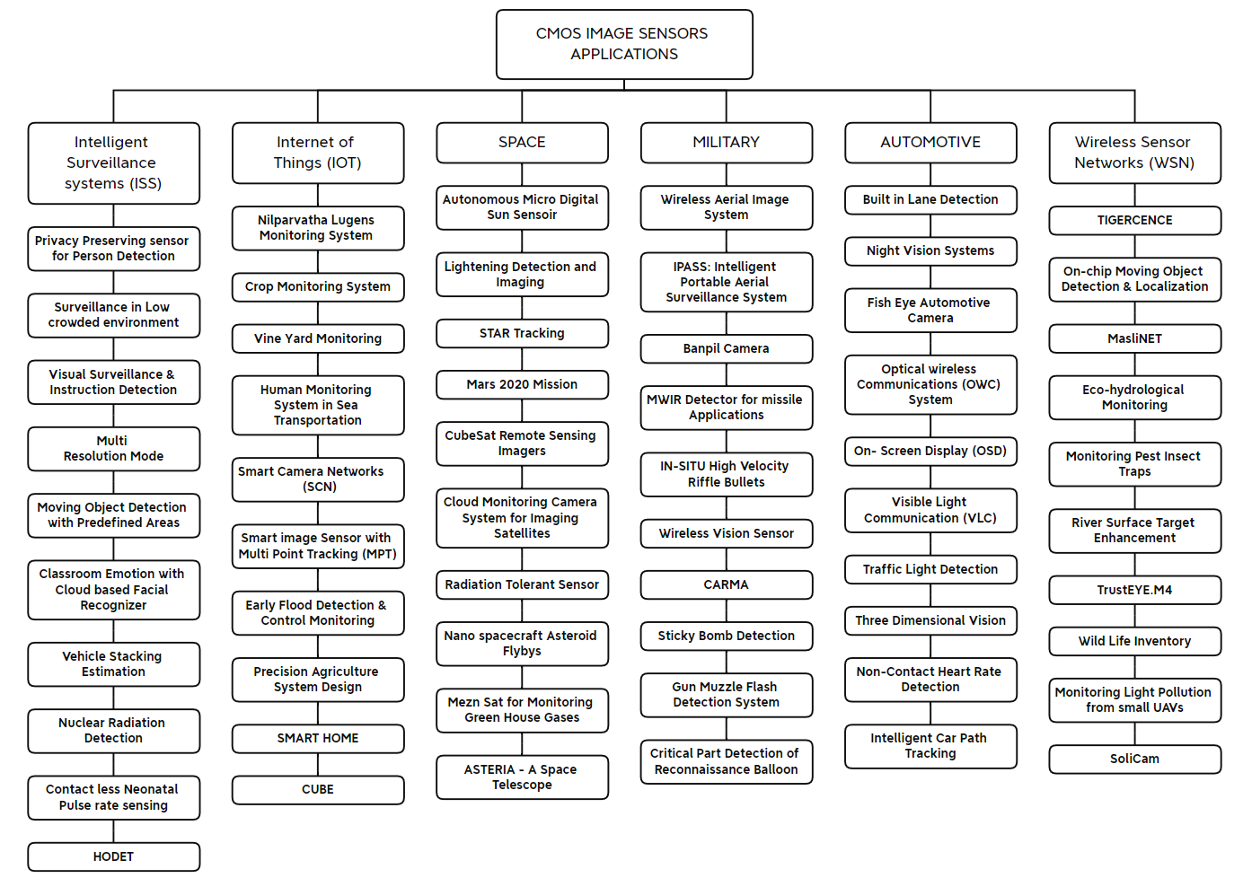
Figure 4. Classification of CMOS image sensor
Over the years, applications using digital cameras have become increasingly convenient and reliable, resulting in their widespread usage and numerous benefits for humanity. Since the 1980s [1], with the development of high technology, significant changes have been made to traditional film cameras.
Electrically writable and controllable FLASH ROMs, coupled with the emergence of low-power, low-price CMOS cameras, have propelled digital cameras into a brand-new era. The internal device of a digital camera has changed considerably compared to traditional film cameras. Under the control of the electronic shutter, a color CMOS camera captures an image and stores it in DRAM before transferring it to FLASH ROM for storage. The storage capacity of a digital camera relies on both the compression level of the image data and the size of the FLASH ROM. Similar to changing a film, users can expand the storage capacity of their digital cameras by swapping out the ROM with a PCMCIA card. Transferring digital image data from the camera to a computer's hard disk significantly simplifies photo storage, retrieval, processing, editing, and transmission.
1.1. ISS (Intelligent Surveillance Systems) CIS applications
For security reasons, surveillance systems have become a part of everyday life to prevent theft and attacks and to help police arrest criminals or thieves. The advanced integration capabilities of CMOS technology make it possible to merge digital circuits into a single chip [7]. This unique feature allows it to offer significant advantages in producing high-definition monitoring images with optimal brightness and crystal-clear details. In particular, higher resolutions can provide even more benefits, making it an ideal choice for handling the large data volumes associated with high-definition monitoring.
However, due to privacy issues, the camera cannot be placed in the bathroom, so it is impossible to monitor the fall of the elderly. Most people feel uncomfortable recording videos in public places, which is why someone recently concerned about privacy policy. It is difficult to determine the difference between the ordinary cameras and the private cameras. The data protection sensor can detect the position of a person by distinguishing the brightness of the background and the brightness of an object in one dimension. The sensor can detect people who fall or stand by maintaining a vertical position and detect other people by maintaining a horizontal position.
A low-power and intelligent CIS suitable for low-traffic areas has been developed by Habibi et al. [4]. The system captures images and features a difference detector inside the pixel to detect any variations in the image over time. Identifying pixels with zero difference and high pixel values enables person detection within the system, indicating when someone enters the frame. The circuit's change window recognizes significant time changes in the pixels. This image sensor node employs a UCAM camera to capture images and can transmit wireless signals to a sensor network to signal an intruder at the image sensor node.
Kim et al. [4] developed a multi-resolution mode CMOS image sensor (CIS) specifically designed for intelligent surveillance system (ISS) applications. This sensor can adjust its image resolution to lower levels during less intensive monitoring modes and then switch to higher resolutions during high monitoring or secure mode. The CIS's adaptive resolution capability significantly decreases power consumption for the always-on surveillance system.
1.2. Space
Image sensors are widely used for space applications, mainly within sensors and optical payloads [8]. At present, among the main remote sensing imaging technologies of Earth observation satellites, infrared remote sensing technology equipment is complex and expensive. Microwave radiometer is usually only suitable for low-resolution data acquisition in a large range (such as local sea area, desert, or geological structure). The radar system is heavy and complex, which requires large power, data transmission rate, and storage capacity. At the same time, it is still difficult for these devices to realize miniaturization.
At present, optical imaging technology (mainly visible light) will be the main means for nano-satellites to complete the Earth observation mission for those weighing less than 10kg. In the visible light system, solid imaging devices (such as CCD) are widely used in the electronic optical system for remote sensing imaging. CMOS imaging devices have a broad application prospect in micro-nano satellites due to their own advantages.
In 1998, Surrey University of the United Kingdom tried the Vision V M5426CMOS camera module in the T MSAT small satellite with a resolution of 382 × 287 achieved satisfactory results [9]. Similar to the requirements for on-board computers, CMOS miniature cameras should also have the function of radiation protection, mainly to prevent single event rollover (SEU). At present, CMOS image sensors with high integration are mostly integrated with SRAM and other devices that may cause single ion inversion. It is necessary to further study the space availability of CMOS miniature camera system by means of radiation experiments. To determine its adaptability to aerospace applications. At present, in the field of remote sensing imaging, the application of CMOS image sensor is still in its infancy, which is related to the relatively small number of high-resolution and high-performance CMOS APS products and the technology needs to be further mature, and also because the technology of the device applied to space has not yet developed and matured, and its adaptability to space environment needs to be further investigated.
1.3. Medical
Biosensors are assuming an ever more significant role in bioscientific applications in the modern world, and there is an expectation that advanced sensors will replace conventional bioanalytical systems due to their enhanced efficiency, sensitivity, and ease of use [10]. The potency of CMOS technology for developing molecular diagnostic systems stems from its versatility and high integration capabilities. Several examples of CMOS sensor applications are shown in the Figure.
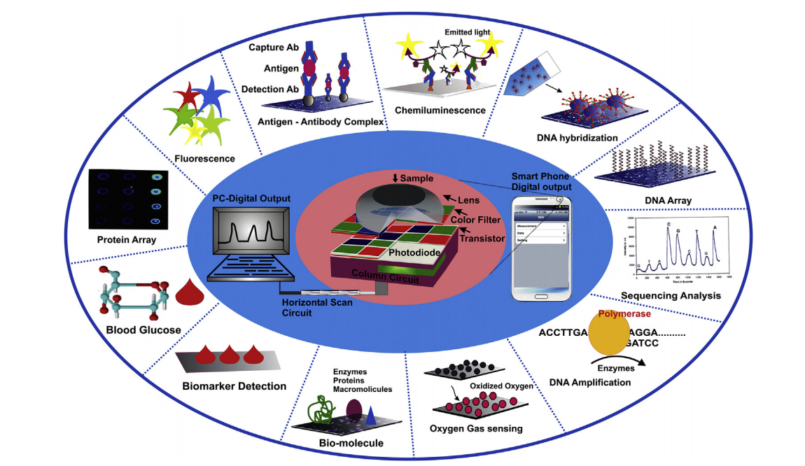
Figure 5. CMOS sensor based on various biomolecular diagnoses
DNA-DNA hybridization is a crucial genetic analysis technique that utilizes sequence similarity to identify target genes. Although Southern hybridization is a frequently employed method with multiple detection steps, it necessitates highly specialized personnel and can take several hours to execute. To overcome these limitations, microarray technology has been developed for DNA and RNA hybridization, enabling analysis with smaller sample sizes, less waste, and shorter processing times. However, the cost of array readers limits their widespread use.
Despite this limitation, microarray technology offers several advantages over traditional southern hybridization, including higher throughput and improved accuracy. Microarrays can analyze thousands of genes simultaneously, providing researchers with a powerful tool for gene expression profiling, drug discovery, and disease diagnosis. Recent advancements in microarray technology have increased its sensitivity and specificity, allowing for more precise and accurate analysis. These advancements also include the use of portable microarray readers, making diagnostics accessible in remote locations.
Overall, microarray technology represents a major advancement in DNA and RNA hybridization, offering improved efficiency and accuracy over traditional techniques. While cost limitations remain an issue, continued advancements in technology are making microarray analysis more accessible and affordable, paving the way for increased use in research and clinical applications.
On the other hand, CMOS image sensors have become promising optical reader for DNA hybridization. By fixing pre-marked single-chain DNA probes onto a matrix chip with a micro-point instrument, CMOS sensors integrated with silicon chips have been developed as carrier materials for the construction of silicon-based DNA micro-array chips. This represents a significant step forward in DNA-DNA hybridization based on CMOS sensors.
4. Advances in CMOS image sensors
Semiconductor-based DNA sequencing systems available in the commercial market are promising innovations for biomedical applications. Furthermore, several sensors have been suggested for DNA-DNA hybridization, gene amplification, and gene sequencing. The efficiency of CMOS sensors enables high sensitivity, quantitative and qualitative analysis, ease of use, portability, and speed. They offer several advantages, including data storage and transmission, sensor integration, reduced workforce requirements, increased profitability, and the ability to perform multiple analyses. Overall, CMOS sensors are becoming an increasingly important tool in molecular biology and biomedical applications. Their versatility and ease of use make them attractive for a wide range of research and diagnostic applications, contributing to the development of more efficient and accurate diagnostic tests and bioanalytical systems. Recent advances in CMOS image sensor technology have opened up new possibilities for image capture and processing. Three of the most significant advances are backside illumination, global shutter, and 3D imaging.
Backside illumination (BSI) is a technique that involves flipping the sensor so that the light enters from the backside rather than the front. This allows for more photons to reach the photodiodes, resulting in better sensitivity and lower noise. BSI has become increasingly popular in smartphones and other consumer devices, where low-light performance is critical.
Global shutter is another recent advance that addresses a common problem with CMOS sensors: rolling shutter distortion. Rolling shutter distortion occurs when the sensor captures different parts of the image at slightly different times, resulting in skewed or distorted images. Global shutter solves this problem by capturing the entire image at once, eliminating rolling shutter distortion.
Finally, 3D imaging is an emerging technology that uses time-of-flight or structured light to capture depth information along with the image. This allows for more accurate and detailed 3D reconstructions of objects and scenes.
Each of these advances has significant performance improvements over traditional CMOS sensors. BSI sensors can capture images in low-light conditions with less noise, while global shutter sensors produce more accurate and distortion-free images. 3D imaging provides a new dimension of information for applications such as robotics, augmented reality, and medical imaging. These advances have already had a significant impact on many industries. BSI sensors are now ubiquitous in smartphones, and global shutter sensors are becoming more common in industrial and scientific applications. 3D imaging is still in its early stages, but its potential applications are vast.
In the future, we can expect to see further improvements in CMOS image sensor technology, including higher resolutions, faster frame rates, and more advanced signal processing. These advances will enable new applications in fields such as autonomous vehicles, virtual reality, and machine vision. Overall, the recent advances in CMOS image sensor technology have opened up new possibilities for image capture and processing, and their impact is likely to continue to grow in the coming years.
5. Conclusion
To provide a more comprehensive conclusion, it is essential to highlight the significance of CMOS image sensors in the electronic industry. CMOS image sensors have revolutionized the field of digital imaging, enabling high-quality image capture in various applications. Their low power consumption, small size, and weight, along with their high integration, fast readout speed, and low cost, have made them the preferred choice in the market. The development of CMOS image sensors has several main trends at present.
Firstly, there is a focus on achieving high frame rates through the flexible access provided by CMOS technology [11]. By reading out only a small area of interest on the photosensitive surface, frame rates can be increased.
Secondly, there is a push for reduced noise levels. While high-performance CCDs used for scientific research can achieve impressive noise levels of 3-5 electrons, CMOS image sensors have a higher noise level ranging from 300-500 electrons.
Finally, there is a drive towards creating multi-functional, intelligent, single-chip digital cameras. CMOS image sensors are particularly advantageous for this due to their high integration capability. It is theoretically possible to integrate all required functions for image sensors, such as vertical and horizontal displacement, timing control, correlated double sampling, and analog-to-digital conversion onto a single chip, thus creating a single-chip camera. This level of integration is made possible through large-scale integrated circuit technology [12].
In summary, CMOS image sensors are developing towards high sensitivity, high resolution, high dynamic range, high frame rates, integration, miniaturization, low power consumption, digitization, and intelligence [13]. Researchers are primarily focusing on improving the overall performance of CMOS image sensors, especially CMOS active pixel sensors (CMOS-APS), by reducing the size of pixels, adjusting CMOS process parameters, integrating clock and control circuits, signal processing circuits, A/D circuits, image compression circuits, etc. with the image sensor array, and producing color filters and microlens arrays. This is in order to achieve a low-cost, low-power, highly integrated single-chip imaging microsystem.
References
[1]. Voinigescu, Sorin. High-Frequency Integrated Circuits. Cambridge University Press. pp: 164,2013.
[2]. Freitas L, Morgado-Dias F . A CMOS Image Sensor with 14-Bit Column-Parallel 3rd Order Incremental Sigma-Delta Converters J. Sensors and Actuators A Physical, 2020, 313:112162.
[3]. Zhu MX, Tang PY, Huang ZL, et al A multi-channel CMOS image monitoring system based on DSP and FPGA J.Electronic Design Engineering, 2011, 19 (14): 3.
[4]. Sukhavasi S B , Sukhavasi S B , Elleithy K , et al. CMOS Image Sensors in Surveillance System Applications J. Sensors, 2021, 21(2):488.
[5]. Zhang YM, Xu JT, Nie KM, Liu CJ, Yang YL, Wang H. Analysis and optimization design of control signal line parasitic effects on streaking phenomenon in CMOS image sensor. Microelectronics Journal 133(2023). March 2023.
[6]. Theuwissen A . CMOS image sensors: State-of-the-art and future perspectives[C]// ESSCIRC 2007 - 33rd European Solid-State Circuits Conference. IEEE, 2008.
[7]. Liu YQ, Wu ZJ, Liu CJ, et al. Research on an automatic exposure algorithm for CMOS image sensors used in security monitoring J. Semiconductor Optoelectronics, 2017,38 (02): 283-287. DOI: 10.16818/j.issn1001-5868.2017.02.027.
[8]. You Z, Li T, Application of CMOS image sensors in space technology J. Optical Technology, 2002, 28 (1): 5.
[9]. O. Saint-Pé, Magnan P , M. Bréart de Boisanger, et al. High-performance imagers for space applications: The strong benefits of CMOS image sensors processes J. Nuclear Instruments & Methods in Physics Research, 2009, 610(1):230-233.
[10]. Devadhasan S . Overview of CMOS image sensor use in molecular diagnostics J. Current applied physics: the official journal of the Korean Physical Society, 2015, 15(3).
[11]. Li JJ, Du YG, Zhang LH, Liu QL, Chen JR. Research Progress of CMOS Image Sensors J. Laser and Optoelectronics Progress, 2009, 46(04): 45-52.
[12]. Shilin V. A., Skrylev P.A., Stempkovsky A.L. Optimum design of CMOS imagers C.SPIE, 2003, 5036: 157~164.
[13]. M. Bigas, E. Cabruja, J. Forest et al.. Review of CMOS image sensor J.Microelectronics Journal, 2006, 37: 433~451.
Cite this article
Shi,C. (2023). Applications of CMOS image sensors: Applications and innovations. Applied and Computational Engineering,11,95-103.
Data availability
The datasets used and/or analyzed during the current study will be available from the authors upon reasonable request.
Disclaimer/Publisher's Note
The statements, opinions and data contained in all publications are solely those of the individual author(s) and contributor(s) and not of EWA Publishing and/or the editor(s). EWA Publishing and/or the editor(s) disclaim responsibility for any injury to people or property resulting from any ideas, methods, instructions or products referred to in the content.
About volume
Volume title: Proceedings of the 2023 International Conference on Mechatronics and Smart Systems
© 2024 by the author(s). Licensee EWA Publishing, Oxford, UK. This article is an open access article distributed under the terms and
conditions of the Creative Commons Attribution (CC BY) license. Authors who
publish this series agree to the following terms:
1. Authors retain copyright and grant the series right of first publication with the work simultaneously licensed under a Creative Commons
Attribution License that allows others to share the work with an acknowledgment of the work's authorship and initial publication in this
series.
2. Authors are able to enter into separate, additional contractual arrangements for the non-exclusive distribution of the series's published
version of the work (e.g., post it to an institutional repository or publish it in a book), with an acknowledgment of its initial
publication in this series.
3. Authors are permitted and encouraged to post their work online (e.g., in institutional repositories or on their website) prior to and
during the submission process, as it can lead to productive exchanges, as well as earlier and greater citation of published work (See
Open access policy for details).
References
[1]. Voinigescu, Sorin. High-Frequency Integrated Circuits. Cambridge University Press. pp: 164,2013.
[2]. Freitas L, Morgado-Dias F . A CMOS Image Sensor with 14-Bit Column-Parallel 3rd Order Incremental Sigma-Delta Converters J. Sensors and Actuators A Physical, 2020, 313:112162.
[3]. Zhu MX, Tang PY, Huang ZL, et al A multi-channel CMOS image monitoring system based on DSP and FPGA J.Electronic Design Engineering, 2011, 19 (14): 3.
[4]. Sukhavasi S B , Sukhavasi S B , Elleithy K , et al. CMOS Image Sensors in Surveillance System Applications J. Sensors, 2021, 21(2):488.
[5]. Zhang YM, Xu JT, Nie KM, Liu CJ, Yang YL, Wang H. Analysis and optimization design of control signal line parasitic effects on streaking phenomenon in CMOS image sensor. Microelectronics Journal 133(2023). March 2023.
[6]. Theuwissen A . CMOS image sensors: State-of-the-art and future perspectives[C]// ESSCIRC 2007 - 33rd European Solid-State Circuits Conference. IEEE, 2008.
[7]. Liu YQ, Wu ZJ, Liu CJ, et al. Research on an automatic exposure algorithm for CMOS image sensors used in security monitoring J. Semiconductor Optoelectronics, 2017,38 (02): 283-287. DOI: 10.16818/j.issn1001-5868.2017.02.027.
[8]. You Z, Li T, Application of CMOS image sensors in space technology J. Optical Technology, 2002, 28 (1): 5.
[9]. O. Saint-Pé, Magnan P , M. Bréart de Boisanger, et al. High-performance imagers for space applications: The strong benefits of CMOS image sensors processes J. Nuclear Instruments & Methods in Physics Research, 2009, 610(1):230-233.
[10]. Devadhasan S . Overview of CMOS image sensor use in molecular diagnostics J. Current applied physics: the official journal of the Korean Physical Society, 2015, 15(3).
[11]. Li JJ, Du YG, Zhang LH, Liu QL, Chen JR. Research Progress of CMOS Image Sensors J. Laser and Optoelectronics Progress, 2009, 46(04): 45-52.
[12]. Shilin V. A., Skrylev P.A., Stempkovsky A.L. Optimum design of CMOS imagers C.SPIE, 2003, 5036: 157~164.
[13]. M. Bigas, E. Cabruja, J. Forest et al.. Review of CMOS image sensor J.Microelectronics Journal, 2006, 37: 433~451.