


1. Introduction
1.1. Background
As the rapid advancement of the electronic industry, the requirements for instruments and circuits are increasing rapidly in recent years. An absolute value circuit is a high-precision rectifier. Compared with the general rectifier circuit, it uses the high gain characteristics of the operational amplifier to improve the rectifier accuracy [1]. The advantage of an absolute value circuit is that the high gain characteristics of the operational amplifier can be used to improve the rectification accuracy [2]. Absolute value circuit has found an increasingly wide utilization in digital signal processing. They can be used in many electronic instruments. In terms of bipolar signal instrumentation, absolute value circuits make it less necessary to use gain-polarity-switched amplifiers [3]. Traditional designs of absolute value circuits used two op-amps and two precision resistors. Jones, David, and Mark Stitt optimized the circuit with an op-amp and an IC difference amplifier, with the advantages of no resistor adjustments from users and suitable for precision split supply operation [4].
In addition, a difference amplifier can enhance performance and lower the power of traditional absolute value circuits. Early design used full-wave rectifier circuits including two fast operational amplifiers and five precision resistors. In contrast, the improved design includes a dual-channel difference amplifier to provide a precision absolute value output, and the design has no external components. Optimizing the circuit lowers cose and reduces complexity by eliminating the need for dual power supplies and great performance external components, eliminating crossover recovery problems by implementing the difference amplifier solution, and lowering power consumption by using a single IC [5].
Digital Signal Processing (DSP) using digital processing to perform various signal-processing operations. When compared to analog processing, the use of digital computers in signal processing has various benefits, including data reduction and error detection and correction in transmission [6]. Digital technologies like wireless communications and digital telecommunications also depend on digital signal processing [7]. DSP works well with both static and streaming data.
1.2. Recent progress
One of the main design requirements is energy minimization, important for almost all electronic systems especially for portable electronic systems like smartphones and different devices [8]. Reaching this minimization with minimal performance penalty is highly desired. Digital signal processing blocks are a key component of these portable devices for various multimedia applications [9].
The design community has become more interested in spike sorting algorithms as a result of the advancement of neural signal acquisition technologies [10]. An absolute value detector is one of the most widely used algorithms used for detecting spikes [11].The community responsible for designing absolute value detectors compares the incoming signal to the predetermined threshold [11].
The paper [12] first suggests three different topologies. The first topology makes use of a comparator, a truth table for the absolute value of the 2’s complement format, and a combinational logic circuit. The second design comprises a comparator, a set of half adders, and transmission gates. The combinational logic circuit by truth table of 2’s complement and a cascade of full adders connected in series with the carry-out signal make up the third design. The report then compares the overall stage count and transistor consumption of each circuit. mainly because the second circuit uses the least amount of transistors and has the fewest steps. In the end, it decides to focus the critical path delay’s and energy consumption’s optimization on the second circuit.
In the paper [13], a 4-bit absolute value detector with low latency and low energy consumption is designed to cope with the increasing demand of equipment developing with the electronics industry [14].MUX, adder, and comparator make up the detector. This study redesigns the XOR gate using the transmission gate logic, which significantly enhances the performance of the XOR gate, based on the logical effort theory. It also estimates the logical effort and parasitic delay at each stage of the detector. In the complement format of 2, it is feasible to calculate the absolute value of a 4-bit input digit, compare it to a threshold value, and draw conclusions.
1.3. This paper
In this paper, different applications of absolute value circuit are introduced based on three articles which separately show its applications in biological signal processing, analog to digital conversion and chip signal processing. Absolute Value Circuit have different structures that can be modified to meet different need.
2. Theoretical analysis of 4-bit absolute value detector
As neural signal acquisition systems develop recently, the design community shifts its interest to spike-sorting algorithms [10]. The input signal will be compared to a threshold previously setted by the absolute-value detector. The absolute value circuit can convert dual-polarization data into single-polarization data. In the process of computer acquisition and processing, the symbol part should be removed, and the digital-analog conversion window should be expanded to improve the accuracy [15].
The basic diagram of an Absolute-value detector is shown by Figure 1.
Figure 1. Absolute value detector.
The absolute-value detector has two main components i) researching and finding the neural signal’s magnitude (x [n]) ii) comparing this magnitude to the given threshold value. If the threshold is greater than the magnitude of the signal output should display a ‘0’ (high logic value), otherwise the output should be a ‘1’ (low logic value).
The value of input ranges from negative seven to seven, whose format will be given as 2’s complement. Although −8 can be represented in 2’s complement using 4 bits, this study can assume that this will never occur at input. Therefore, the magnitude of the signal compared to the given 3-bit threshold value in the comparator will always be 3 bits.
As Figure 2, the comparator is used to compare the value of the 3-bit magnitude of signal and the given threshold. To compare the most significant bits of the two numbers is the strategy here . If one is greater than the other, the comparator understands that number is greater. If the two numbers are equal, the comparator will move to the second most significant bit, and so on.
Figure 2. A 4-bit magnitude comparator.
3. Applications of absolute value circuits
3.1. Biological signal processing applications
The absolute value might be very important in the biological signal processing process. To achieve a high signal-to-noise ratio, this field needs low energy consumption, great precision, and a wide dynamic range. The article [16] proposes a nano power high precision absolute value circuit based on subthreshold MOS transistors, with six MOS transistors, one bias voltage, two bias currents, and lower, which can be used in biomedical signal processing applications. The circuit can cleanly output a low level signal after rectifying it.
The goal of the work is to create or improve a precision absolute value circuit that is based on conventional AB rectifiers but has greater accuracy, better output peak symmetry, and more stable temperature. The proposed absolute value circuit used in biological signal processing applications is shown in Figure 3.
Figure 3. The proposed absolute value circuit used in biological signal processing.
The transistors M4 and sthece of current I-B1 produce a voltage, which is named transistor M3’s gate-biasing-voltage, allowing the transistor to operate in class-AB by lowering its threshold voltage and obtaining a subthreshold region. The operation of the circuit is as Figure 4. Since both when Iin >0 and when Iin <0, the output value of the current is the absolute value of Iin, the relationship can be expressed as: Iout = |Iin|. Therefore, the circuit can be operated as an absolute value circuit.
Figure 4. The operation procedure of the proposed circuit.
The issue of inadequate matching characteristics between current mirror devices will result in an output waveform that is not symmetrical because the first polarity signal’s amplitude is not equal to the second polarity signal’s amplitude. The bias voltage is supplied to solve this by increasing the bias of current mirror M1-M2 to improve output waveform.
After testing the circuit simulation, some results can be known. The transfer characteristics of direct of the absolute value with its zero crossing region are shown in Figure 5. The figure shows a good linear relationship between Iin and Iout, and they are strictly equal, which shows good DC current characteristics.
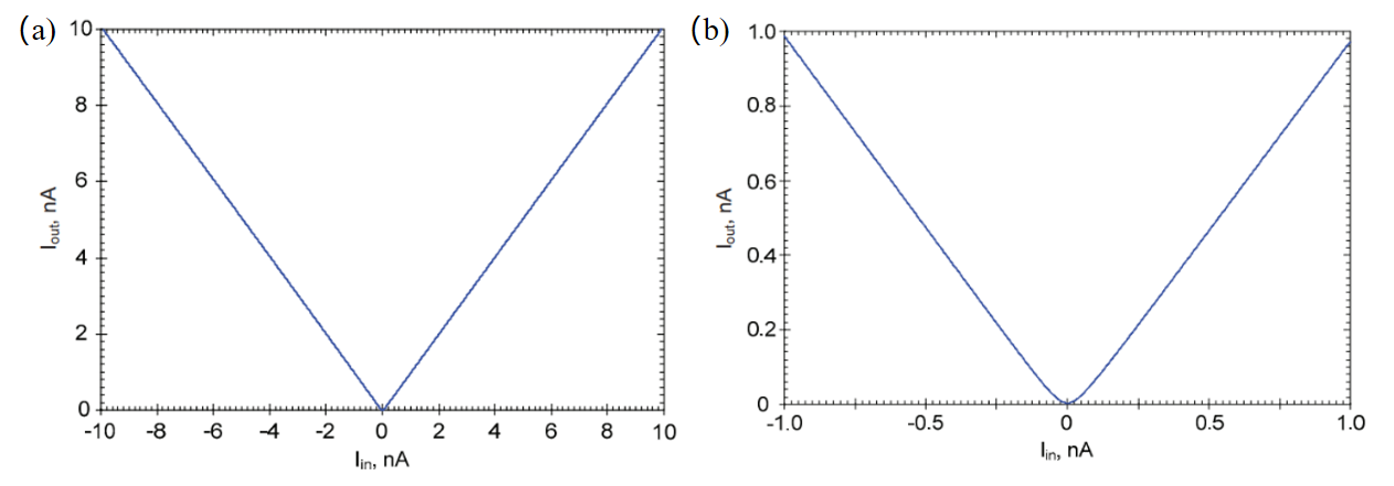
Figure 5. The transfer characteristics of direct current of the absolute value, (a) Analog results for direct current transfer characteristic, (b) Zero crossing’s zooming.
Performance of the suggested absolute value at various temperatures at 1 Hz frequency are shown in Figure 6, which shows the circuit have good temperature stability from 27℃ to 40℃.
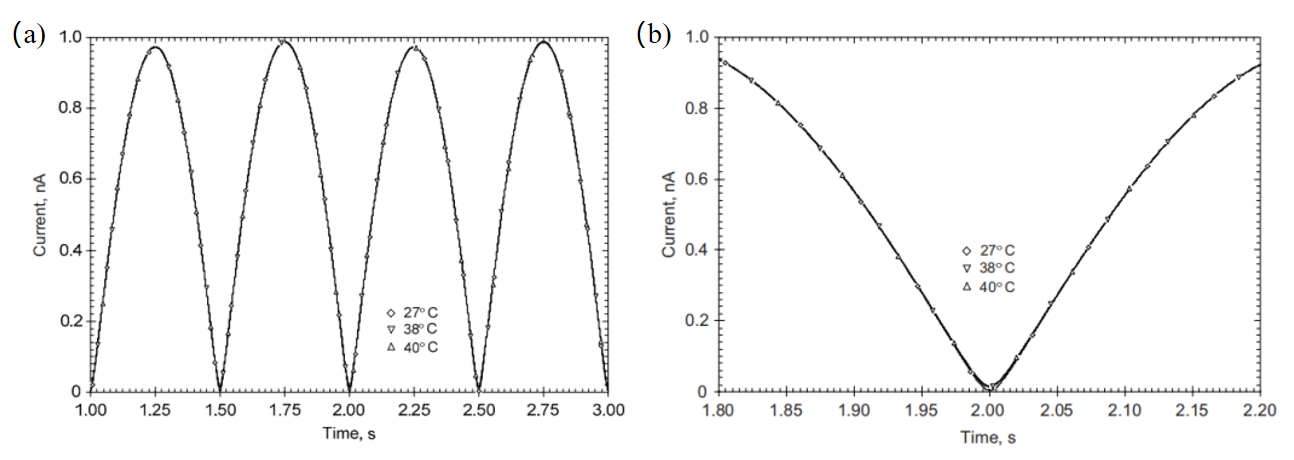
Figure 6. Performance of the suggested absolute value at various temperatures at 1 Hz frequency, (a) Simulated results for suggested absolute value circuit’s operation at 1 Hz frequency at different temperatures, (b) Zoming of one of the zero points(2.00).
Given that biological signals are typically relatively tiny and improved circuit precision is needed, the absolute value circuit is presented to make it more suitable for signal processing applications in biology field. Additionally, the accuracy of the identification of biological signals depends on the symmetry of each output waveform’s peak.
3.2. Analog to digital conversion
Through A/D converters (ADCs), analog signals can be converted into digital signals to attain the ability of being processed by software. The article [17] shows that, for the purpose of A/D conversion, the absolute value circuit with operational amplifier can realize signal fidelity transform and the circuit is simple and cheap.
The usual analog converter needs to input information is the DC voltage type, which means that the signals need to be converted into a DC voltage for delivery to the analog-to-digital converter. Such signal transformation and transmission can be realized by using the absolute value output, absolute value multiplier, negative value output and the same type of circuit.
There are three methods to design an absolute value circuit for AD conversion. The first one is the absolute value output circuit, shown in Figure 7. The circuit in the dashed box has YF 1 as the core, and the output point C is negative when input point A is positive and output point C is zero when input point A is negative. The circuit outside of the dashed box constitutes the adder.
where there are three addresses, you should insert numbered superscripts 1, 2 and 3 to link surnames to addresses and then insert footnotes 4 and 5. Note that the first footnote in the main text will now be number 6.
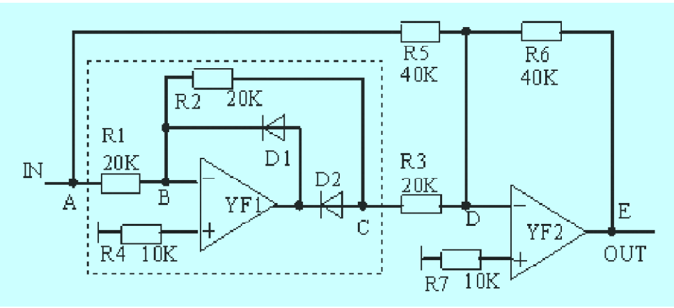
Figure 7. Absolute value output circuit.
The second one is the negative value output circuit, which is shown in Figure 8. In the control and analog transformation system, changing the positive and negative signals into the negative value of equal magnitude is sometimes necessary, which also belongs to the absolute value transformation.
The circuit in the dashed box has YF 1 as the core, and the output point C is negative when input point A is positive and output point C is zero when input point A is negative. The circuit outside of the dashed box constitutes the adder. Suppose the input signal of point M is negative. In that case, D01 is off, D02 is on, the output voltage of YF 02 is fed back to point N and makes it equal to the potential of point M, and the two-stage operational amplifiers form a series voltage follower, so that the output of point W OUTW= INM. However, due to the isolation and delay of YF 02, YF 01 will undergo a weak high-frequency oscillation during the negative half-wave input of the AC signal. Add R05 and C1 negative feedback to eliminate the oscillation. Because the C1 capacitor is very small, it has no effect on the power frequency level signal. No oscillation occurs when the input signal is DC.
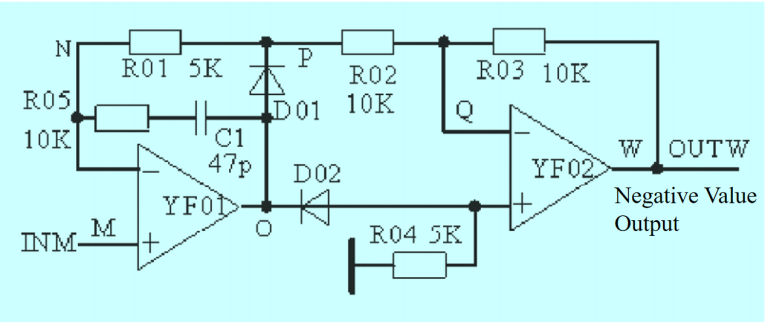
Figure 8. Negative value output circuit.
The last one is the absolute value sampling for a multiplexed system, which is shown in Figure 9. The three-way absolute value adder processing and transformation can achieve high-fidelity feedback information transmission. The waveform can be sent to the analog to digital converter into digital signal output and directly to the feedback control circuit to achieve a more accurate and larger range of control.
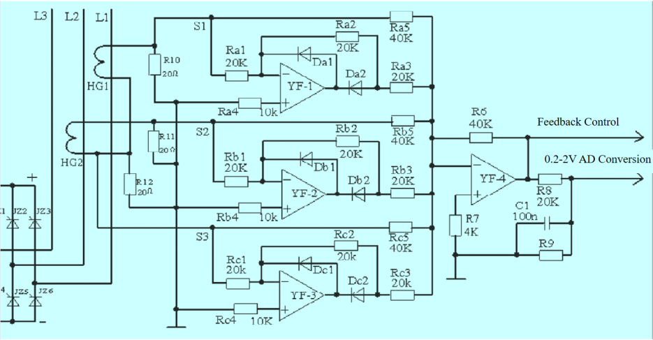
Figure 9. Three-way absolute value adder sampling circuit.
After verification, the above circuit built by the operational amplifier realizes the high fidelity transformation of the signal well, and the circuit is simple and cheap. A highly accurate digital AC ammeter can be made with a current transformer, equipped with the circuit shown in Figure 7 and properly reducing the output to the analog-to-digital converter. Therefore, the absolute value circuit built with the operational amplifier plays an important role in the data sampling, measurement and display link in the field of automatic control.
3.3. Chip signal processing applications
In the paper, they finally optimized a 4-bit value detection to have a minimum latency energy 50% longer than its minimum latency.
In the paper, the circuits are designed using static CMOS design theory and pass transistor circuit theory. After obtaining an optimized design, they applied logic workload calculations to calculate the circuit’s minimum delay and determine each gate size values for specific logic component. Ultimately, they sacrificed a little delay for a lot of energy reduction. The main design idea is shown in Figure 10.
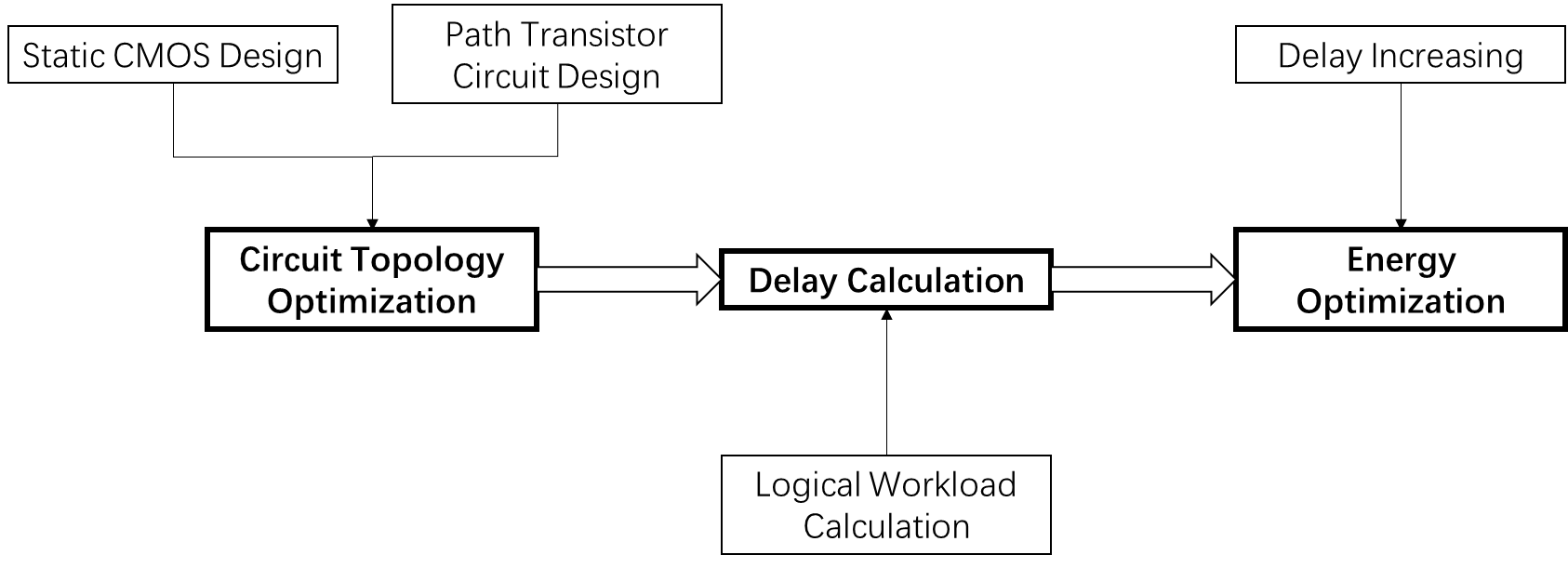
Figure 10. 4-bit value detection optimization flowchart.
The whole circuit has two main parts, finding the magnitude value of a 4 bits random variable inputs, and the second compares the calculated value with a threshold value and the greater value will be the output. In the case, there is only 4-bits value, and the most significant bit (MSB) is a sign bit, so they only have 3-bits value to represent its magnitude. If the value is positive, the magnitude is just the 3-bits value itself in binary. If the value is negative, then this study needs to flip all bits and add 1 to get the magnitude value. Then it comes to the comparator. In the comparator it will compare the calculated result from the first step and compare it with the threshold. The final output is 1 if the value is larger than the threshold value and 0 if the value is less than or equal to the threshold value. The detail information as shown in the Figure 11 below.
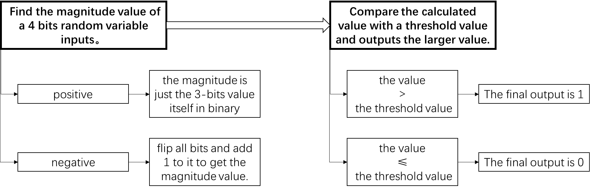
Figure 11. 4-bit value detection schematic.
In-Circuit Topology Optimization, they introduced a better half adder circuit design, a more static transmission gate multiplexer (MUX) design, and a comparator design, all of which are best fits to the 4-bit Absolute-Value Detector. Because of the optimization circuit design introduced in Circuit Topology Optimization, the total critical path delay in Delay calculating is smaller than a traditional design. Then, in energy optimization they sacrificed the delay a little bit to get a minimum energy consumption, and eventually got a minimum energy consumption which is 78% reduction.
According to all the optimization as mentioned above the absolute value detector has less delay and lower energy consumption.
A 4-bits Absolute-Value Detector can be used in plenty of areas, most commonly in a chip ALU unit. Since this circuit consists of adder and comparator circuit, which are also broadly used in chip’s ALU unit, a good optimization of 4-bits absolute value detector is very useful.
4. Conclusion
Absolute value circuits are widely used in electronic industries like digital signal processing applications. This paper introduced three different absolute value circuit for different uses. The absolute precision value circuit is optimized based on conventional class-AB rectifiers in biological signal processing applications to meet the demands for better precision, better symmetry of each output peak, and more stable temperature, which the biological signal field requires. In AD Conversion applications, three different absolute value circuit are proposed to meet the need for AD conversion. In chip signal processing Applications, the paper finally used static CMOS theory and pass transistor circuit theory to optimize a 4-bit value detection to have a minimum latency energy 78% longer than its minimum latency.
References
[1]. Cao, Y 1984 Absolute Value Circuits and the Application in the A/D Converter. Process Automation Instrumentation, (2), 5.
[2]. Gan, X 2006 Principles and design of integrated circuits. Peking University Press.
[3]. Barker, R. W. J., & Hart, B. L 1989 Precision absolute-value circuit technique. International Journal of Electronics, 66(3), 445-448.
[4]. Jones, D., & Stitt, M 1997 Precision absolute value circuits. Burr-Brown application bulletin.
[5]. Gerstenhaber, M., & Malik, R 2010 More value from the absolute value circuit-difference amplifier enables low-power, high-performance absolute value circuit. Analog Dialogue, 44-04 Burner, April.
[6]. Broesch, J. D., Stranneby, D., Walker, W 2008 Digital Signal Processing: Instant access (1 ed. Butterworth-Heinemann-Newnes.
[7]. Srivastava, V. M., Singh, & Ghanshyam 2013 MOSFET Technologies for Double-Pole F-the-Throw Radio-Frequency Switch. Springer Science & Business Media.
[8]. Alioto, M 2012 Ultra-low power VLSI circuit design demystified and explained: A tutorial. IEEE Transactions on Circuits and Systems I: Regular Papers, 59(1), 3-29.
[9]. Zendegani, R., Kamal, M., Bahadori, M., et al 2016 RoBA multiplier: A rounding-based approximate multiplier for high-speed yet energy-efficient digital signal processing. IEEE Transactions on Very Large Scale Integration (VLSI) Systems, 25(2), 393-401.
[10]. Veerabhadrappa, R., Ul Hassan, M., Zhang, J., & Bhatti, A 2020 Compatibility evaluation of clustering algorithms for contemporary extracellular neural spike sorting. Frontiers in Systems Neuroscience, 14.
[11]. Yuan, M 2021 An absolute-value detector with threshold comparing for spike detection in the brain-machine interface. Journal of Physics: Conference Series, 2113(1), 012038.
[12]. Jia, Y 2023 Design and Optimization of 4-bit Absolute-value Detector Based on CMOS. Journal of Physics: Conference Series, 2435(1), 012011.
[13]. Du, C., Guo, Y., & Zhang, J 2023 A Low Energy Depletion CMOS Transistor-based 4-bit Absolute-value Detector. Journal of Physics: Conference Series, 2435(1), 012012.
[14]. Poustie, A., Blow, K., Kelly, A., & Manning, R 1998 All-optical binary half-adder. Optics Communications, 156(1-3), 22-26.
[15]. Chandrakasan, A. P., Sheng, S., & Brodersen, R. W 1992 Low-Power CMOS Digital Design. IEEE Journal of Solid-State Circuits, 27(4), 473-484.
[16]. Kumngern, M 2013 Absolute Value Circuit for Biological Signal Processing Applications. 2013 4th International Conference on Intelligent Systems, Modelling and Simulation, Bangkok, Thailand, pp. 601-604.
[17]. Wu, J., Wu, W., & Jia, Q 2012 The Application of Absolute Value Circuit in the A / D Converter. Industrial Applications and Communications.
Cite this article
Sha,B. (2023). 4-bit absolute value detection for digital signal processing applications. Applied and Computational Engineering,12,13-21.
Data availability
The datasets used and/or analyzed during the current study will be available from the authors upon reasonable request.
Disclaimer/Publisher's Note
The statements, opinions and data contained in all publications are solely those of the individual author(s) and contributor(s) and not of EWA Publishing and/or the editor(s). EWA Publishing and/or the editor(s) disclaim responsibility for any injury to people or property resulting from any ideas, methods, instructions or products referred to in the content.
About volume
Volume title: Proceedings of the 2023 International Conference on Mechatronics and Smart Systems
© 2024 by the author(s). Licensee EWA Publishing, Oxford, UK. This article is an open access article distributed under the terms and
conditions of the Creative Commons Attribution (CC BY) license. Authors who
publish this series agree to the following terms:
1. Authors retain copyright and grant the series right of first publication with the work simultaneously licensed under a Creative Commons
Attribution License that allows others to share the work with an acknowledgment of the work's authorship and initial publication in this
series.
2. Authors are able to enter into separate, additional contractual arrangements for the non-exclusive distribution of the series's published
version of the work (e.g., post it to an institutional repository or publish it in a book), with an acknowledgment of its initial
publication in this series.
3. Authors are permitted and encouraged to post their work online (e.g., in institutional repositories or on their website) prior to and
during the submission process, as it can lead to productive exchanges, as well as earlier and greater citation of published work (See
Open access policy for details).
References
[1]. Cao, Y 1984 Absolute Value Circuits and the Application in the A/D Converter. Process Automation Instrumentation, (2), 5.
[2]. Gan, X 2006 Principles and design of integrated circuits. Peking University Press.
[3]. Barker, R. W. J., & Hart, B. L 1989 Precision absolute-value circuit technique. International Journal of Electronics, 66(3), 445-448.
[4]. Jones, D., & Stitt, M 1997 Precision absolute value circuits. Burr-Brown application bulletin.
[5]. Gerstenhaber, M., & Malik, R 2010 More value from the absolute value circuit-difference amplifier enables low-power, high-performance absolute value circuit. Analog Dialogue, 44-04 Burner, April.
[6]. Broesch, J. D., Stranneby, D., Walker, W 2008 Digital Signal Processing: Instant access (1 ed. Butterworth-Heinemann-Newnes.
[7]. Srivastava, V. M., Singh, & Ghanshyam 2013 MOSFET Technologies for Double-Pole F-the-Throw Radio-Frequency Switch. Springer Science & Business Media.
[8]. Alioto, M 2012 Ultra-low power VLSI circuit design demystified and explained: A tutorial. IEEE Transactions on Circuits and Systems I: Regular Papers, 59(1), 3-29.
[9]. Zendegani, R., Kamal, M., Bahadori, M., et al 2016 RoBA multiplier: A rounding-based approximate multiplier for high-speed yet energy-efficient digital signal processing. IEEE Transactions on Very Large Scale Integration (VLSI) Systems, 25(2), 393-401.
[10]. Veerabhadrappa, R., Ul Hassan, M., Zhang, J., & Bhatti, A 2020 Compatibility evaluation of clustering algorithms for contemporary extracellular neural spike sorting. Frontiers in Systems Neuroscience, 14.
[11]. Yuan, M 2021 An absolute-value detector with threshold comparing for spike detection in the brain-machine interface. Journal of Physics: Conference Series, 2113(1), 012038.
[12]. Jia, Y 2023 Design and Optimization of 4-bit Absolute-value Detector Based on CMOS. Journal of Physics: Conference Series, 2435(1), 012011.
[13]. Du, C., Guo, Y., & Zhang, J 2023 A Low Energy Depletion CMOS Transistor-based 4-bit Absolute-value Detector. Journal of Physics: Conference Series, 2435(1), 012012.
[14]. Poustie, A., Blow, K., Kelly, A., & Manning, R 1998 All-optical binary half-adder. Optics Communications, 156(1-3), 22-26.
[15]. Chandrakasan, A. P., Sheng, S., & Brodersen, R. W 1992 Low-Power CMOS Digital Design. IEEE Journal of Solid-State Circuits, 27(4), 473-484.
[16]. Kumngern, M 2013 Absolute Value Circuit for Biological Signal Processing Applications. 2013 4th International Conference on Intelligent Systems, Modelling and Simulation, Bangkok, Thailand, pp. 601-604.
[17]. Wu, J., Wu, W., & Jia, Q 2012 The Application of Absolute Value Circuit in the A / D Converter. Industrial Applications and Communications.