


1. Introduction
Power devices play a critical role in modern technology, including renewable energy systems, electric vehicles, and data centers. However, traditional silicon-based power devices face limitations in terms of efficiency, switching speed, and power density [1]. SiC and GaN power devices, which are based on wide-bandgap semiconductor materials, have emerged as promising alternatives.
SiC and GaN power devices are based on wide-bandgap semiconductor materials that exhibit superior material properties, such as high breakdown voltage, high electron saturation velocity, and high thermal conductivity [2]. As a result, SiC and GaN power devices have shown significant improvements in power density, efficiency, and reliability, making them attractive candidates for a wide range of applications. However, the design and optimization of SiC and GaN power devices present unique challenges that require a deeper understanding of their material properties and device structures.
This review paper aims to provide a comprehensive analysis of SiC and GaN power devices, including their material properties, device structures, and performance characteristics. The paper will also discuss the challenges and opportunities associated with SiC and GaN power devices, as well as their potential applications in various fields. In addition to the existing literature, this paper will also explore recent advances in SiC and GaN power devices, and provide insights into future research directions in this field.
2. SiC Power Devices (SiC MOSFET, SiC JFET, SiC Schottky diode)
SiC power devices, such as SiC MOSFETs, SiC JFETs, and SiC Schottky diodes, offer several advantages over traditional silicon-based devices, including higher efficiency, faster switching speeds, and higher power density. In this section, this paper provide an overview of SiC power device structures and their properties, including Ron-Vbd, efficiency, power loss, electron mobility, threshold voltage, breakdown voltage, switching speed, and reliability. This paper review recent research on SiC power devices, including improvements in performance and reliability, and discuss current and potential applications of SiC power devices.
SiC power devices have garnered significant attention in recent years due to their superior performance compared to traditional silicon-based devices
2.1. MOSFETSiC
MOSFETs and GaN MOSFETs are both wide-bandgap semiconductor devices that offer superior performance compared to traditional silicon-based devices. Figure 1 shows the structure of SiC MOSFETs.
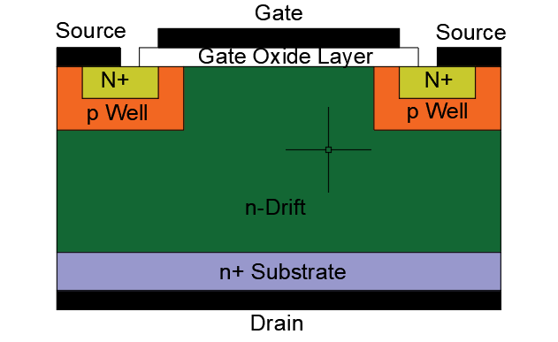
Figure 1. Structure stacks of MOSFET.
However, there are some differences between the two that are worth discussing.
2.1.1. Material properties. SiC has a wider bandgap (3.3 eV) than GaN (3.4 eV), which makes SiC devices more suitable for high-temperature applications. SiC also has a higher thermal conductivity (4.9 W/cmK) compared to GaN (1.3 W/cmK), which makes it easier to dissipate heat from the device.
2.1.2. Breakdown voltage. SiC MOSFETs generally have higher breakdown voltage compared to GaN MOSFETs. This is because SiC has a higher critical electric field strength (2.4 MV/cm) compared to GaN (3 MV/cm) [3].
2.1.3. On-State resistance. GaN MOSFETs generally have lower on-state resistance (Ron) compared to SiC MOSFETs. This is because GaN has a higher electron mobility (2000 cm2/Vs) compared to SiC (900 cm2/Vs).
2.1.4. Switching speed. Both SiC MOSFETs and GaN MOSFETs have fast switching speeds, but GaN MOSFETs are generally faster due to their smaller gate capacitance.
2.1.5. Cost. SiC MOSFETs are currently more expensive compared to GaN MOSFETs, but the cost is expected to come down as production volumes increase.
In terms of technology differences, SiC MOSFETs are typically manufactured using 4H-SiC or 6H-SiC substrates, while GaN MOSFETs are typically manufactured using GaN-on-Si or GaN-on-SiC substrates [4]. MOSFETs also require higher processing temperatures compared to GaN MOSFETs, which can affect the performance of some components in the device.
In summary, SiC MOSFETs and GaN MOSFETs have their own unique advantages and disadvantages, and the choice between the two will depend on the specific requirements of the application. SiC MOSFETs are generally more suitable for high-temperature and high-voltage applications, while GaN MOSFETs are more suitable for high-frequency and high-power density applications.
2.2. JFETS
SiC JFET (Junction Field-Effect Transistor) and GaN JFET are both wide-bandgap semiconductor devices with superior performance compared to traditional silicon-based JFETs.
The following Figure 2 shows the structure of SiC JFET.
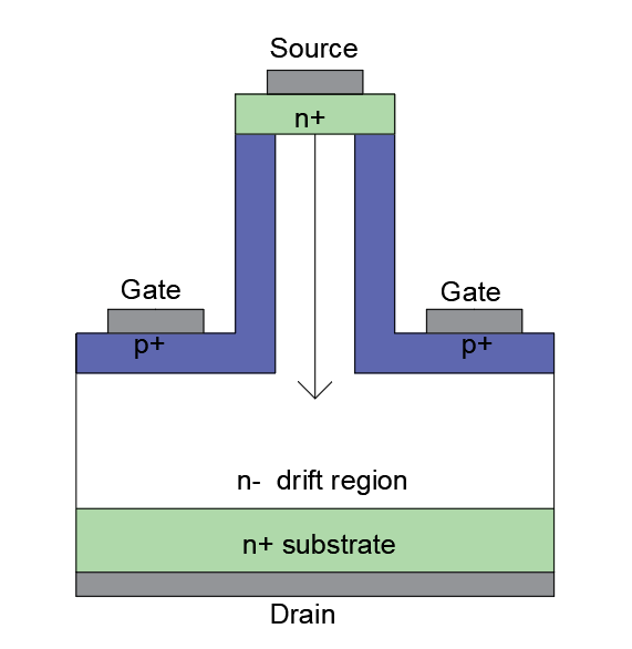
Figure 2. Cross section of the SiC MOSFET.
Here are some differences, advantages, and technical distinctions between the SiC JFET and GaN JFET.
SiC JFETs are made of Silicon Carbide, while GaN JFETs are made of Gallium Nitride. SiC has a higher thermal conductivity and wider bandgap (2.3-3.3 eV) compared to GaN (3.4 eV), which allows for higher operating temperatures and higher breakdown voltages [5].
The JFET structure consists of a p-n junction that controls the flow of current by changing the width of the depletion region. In SiC JFET, the depletion region is controlled by the gate voltage applied to the p-n junction. In contrast, in GaN JFET, the depletion region is controlled by a reverse-biased Schottky gate.
SiC JFETs have a lower gate capacitance, which results in a faster switching speed and reduced switching losses compared to silicon-based JFETs. SiC JFETs also have a higher current density, higher thermal conductivity, and higher temperature capability than silicon-based devices. GaN JFETs, on the other hand, have a lower on-resistance and higher switching speed compared to SiC JFETs.
SiC JFETs require a positive gate voltage to control the depletion region, while GaN JFETs require a negative gate voltage. The gate structure for SiC JFET is a p-n junction, while for GaN JFET, it is a Schottky gate. SiC JFETs have a lower current density and lower breakdown voltage compared to GaN JFETs.
In summary, both SiC JFET and GaN JFET offer superior performance compared to traditional silicon-based JFETs. SiC JFET has a lower gate capacitance, higher current density, and higher temperature capability, while GaN JFET has a lower on-resistance and higher switching speed [6]. technical differences between the two devices lie in their material properties and gate structure.
2.3. Schottky diodes
SiC Schottky diodes and GaN Schottky diodes are both wide-bandgap semiconductor devices that offer several advantages over traditional silicon-based Schottky diodes.
The following Figure 3 shows the structure of SiC Schottky diodes.
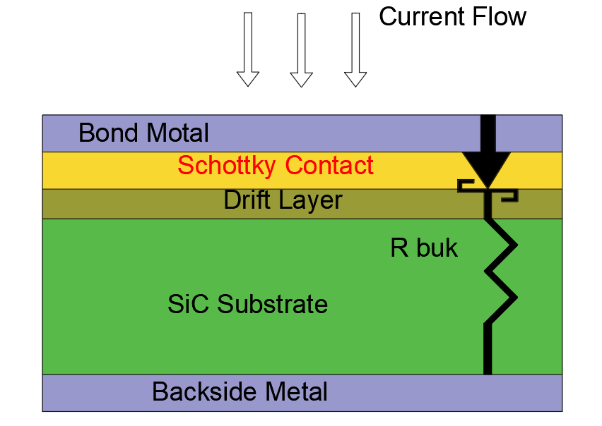
Figure 3. Structure of SiC Schottky diodes.
However, there are some differences in their properties and characteristics.
SiC Schottky diodes have a higher breakdown voltage, lower reverse recovery time, and higher thermal stability compared to GaN Schottky diodes. These properties make them ideal for high-power and high-temperature applications, such as power electronics, aerospace, and automotive industries [7]. Schottky diodes also have a lower forward voltage drop and lower reverse leakage current compared to GaN Schottky diodes, resulting in higher efficiency and reduced power loss.
On the other hand, GaN Schottky diodes have a lower forward voltage drop compared to SiC Schottky diodes, which means they have lower power loss and higher efficiency. They also have a smaller footprint and lower cost compared to SiC Schottky diodes [8].
In terms of technology, SiC Schottky diodes are typically fabricated on a SiC substrate using a metal deposition and thermal annealing process, while GaN Schottky diodes are typically fabricated on a GaN substrate using a metal-organic chemical vapor deposition (MOCVD) process [9].
Recent research has focused on improving the performance and reliability of both SiC and GaN Schottky diodes. For example, researchers have investigated different substrate materials, device structures, and processing techniques to optimize device performance. Improvements have also been made in the design of Schottky contacts and interfaces to reduce reverse leakage current and improve reliability.
Overall, both SiC and GaN Schottky diodes offer advantages over traditional silicon-based Schottky diodes, and their unique properties and characteristics make them suitable for different applications in various industries.
Recent research has focused on improving the performance and reliability of SiC power devices. For example, researchers have investigated different SiC substrate materials, device structures, and processing techniques to optimize device performance [10]. Improvements have also been made in the design of gate structures and interfaces to reduce gate leakage current and improve reliability.
The potential applications of SiC power devices are numerous and diverse. They are suitable for high-power and high-temperature applications, making them ideal for use in aerospace, automotive, and industrial applications [11]. SiC power devices are also being used in renewable energy systems, such as solar and wind power, due to their high efficiency and power density. In addition, SiC power devices are expected to play a key role in the development of next-generation electric vehicles, where they can help increase efficiency and reduce weight.
In summary, SiC power devices offer several advantages over traditional silicon-based devices, including higher efficiency, faster switching speeds, and higher power density. Recent research has focused on improving the performance and reliability of SiC power devices, and they are expected to find wide-ranging applications in various industries in the coming years.
3. GaN power devices
GaN power devices, particularly HEMTs, have gained significant attention in recent years due to their superior performance in terms of switching speed and efficiency. In this section, this paper provide an introduction to GaN power devices, an overview of GaN power device structures and their properties, and a review of recent research on GaN power devices, including improvements in performance and reliability. This paper also discuss current and potential applications of GaN power devices.
3.1. HEMT
Gallium Nitride (GaN) power devices are semiconductor devices that utilize the properties of GaN, a wide-bandgap semiconductor material, for power conversion applications. GaN power devices offer several advantages over traditional silicon-based power devices, including faster switching speeds, higher breakdown voltages, and lower switching losses [12]. Among GaN power devices, the High Electron Mobility Transistor (HEMT) has gained significant attention due to its superior performance characteristics.
3.2. GaN power device structures and properties
GaN power devices have a variety of structures, including lateral and vertical structures. The HEMT is a lateral structure, which is composed of a GaN layer deposited on a substrate with a gate structure [13]. The gate voltage controls the conductivity of the GaN layer, and the device operates in the depletion mode.
The properties of GaN power devices, including electron mobility, breakdown voltage, and on-resistance, depend on the quality of the GaN layer, the gate structure, and the interface between the GaN layer and the substrate [14]. To achieve high-quality GaN layers, various growth techniques have been developed, including Metal-Organic Chemical Vapor Deposition (MOCVD) and Molecular Beam Epitaxy (MBE).
Recent research on GaN power devices has focused on improving their performance and reliability. One approach has been to optimize the GaN layer and the gate structure to reduce on-resistance and improve breakdown voltage. Another approach has been to improve the interface between the GaN layer and the substrate to reduce defects and enhance device reliability [15].
Several studies have demonstrated the potential of GaN power devices in various applications, including power electronics, wireless power transfer, and RF communications [16]. For example, GaN-based power electronics have been used in high-efficiency DC-DC converters, LED drivers, and wireless charging systems.
3.3. Current and potential applications of GaN power devices
GaN power devices have several advantages over traditional silicon-based power devices, including faster switching speeds, higher breakdown voltages, and lower switching losses. These advantages make GaN power devices attractive for a wide range of applications, including power electronics, wireless power transfer, and RF communications.
In power electronics, GaN power devices can be used to improve the efficiency and power density of various systems, such as motor drives, solar inverters, and electric vehicle charging systems. In wireless power transfer, GaN-based systems can be used to transfer power wirelessly over short distances, enabling wireless charging of mobile devices and electric vehicles. In RF communications, GaN power amplifiers can be used to improve the performance of wireless communication systems, such as cellular networks and satellite communication systems.
3.4. Conclusion
GaN power devices, particularly HEMTs, have shown superior performance characteristics in terms of switching speed and efficiency compared to traditional silicon-based power devices. Recent research has focused on improving the performance and reliability of GaN power devices, and several studies have demonstrated their potential in various applications. The continued development and optimization of GaN power devices are expected to lead to further improvements in their performance and reliability, enabling new applications in power electronics, wireless power transfer, and RF communications.
4. Comparison of SiC and GaN power devices
In this section, this paper compare the performance characteristics of SiC and GaN power devices, including efficiency, switching frequency, and thermal management. This paper discuss the advantages and disadvantages of each technology and evaluate current trends of research on SiC or GaN power devices.
SiC and GaN power devices are two of the most promising alternatives to traditional silicon-based power devices. Both SiC and GaN offer several advantages over silicon, including higher efficiency, faster switching speeds, and higher power density. However, there are also differences between these two technologies that make them better suited for different applications.
In terms of efficiency, both SiC and GaN power devices offer significantly higher efficiency than traditional silicon-based devices. SiC devices have a lower on-resistance (Ron) and higher electron mobility, resulting in lower power losses and higher efficiency. GaN devices also offer high efficiency, especially at high frequencies, due to their high electron mobility and low output capacitance.
Switching frequency is another important characteristic of power devices, especially for high-speed applications such as data communication, automotive, and aerospace. GaN power devices have a higher switching frequency than SiC devices due to their smaller gate charge and output capacitance. This means that GaN devices can operate at higher frequencies, resulting in smaller and lighter power electronics systems.
Thermal management is also critical for power devices, as high operating temperatures can cause performance degradation and even device failure. SiC power devices have a higher thermal conductivity than GaN devices, which means that they can handle higher power densities without overheating. However, GaN devices have a smaller thermal resistance, which means that they can dissipate heat more efficiently and have a lower junction-to-case temperature difference.
In terms of cost, both SiC and GaN power devices are more expensive than traditional silicon-based devices, but the cost of these technologies is decreasing as they become more widely adopted. Currently, SiC devices are more expensive than GaN devices, mainly due to the cost of SiC substrates, which are more expensive than GaN substrates.
Overall, SiC and GaN power devices have different strengths and weaknesses, making them better suited for different applications. SiC devices are ideal for high-power, high-temperature applications, such as electric vehicles and industrial motor drives, while GaN devices are better suited for high-speed, low-power applications, such as data communication and aerospace.
5. Perspectives on future development
In this section, this paper provide an overview of research on SiC and GaN power devices and discuss the challenges and opportunities for future development. This paper highlight the importance of addressing reliability issues and reducing costs to facilitate widespread adoption of SiC and GaN power devices.
The development of SiC and GaN power devices has undergone significant progress in recent years, and their potential for use in a wide range of applications has been widely recognized. However, there are still several challenges that need to be addressed to facilitate their widespread adoption.
One of the most significant challenges is improving the reliability of these devices. While SiC and GaN power devices offer superior performance characteristics compared to traditional silicon-based devices, they are also more susceptible to issues such as high-temperature operation, gate oxide breakdown, and current collapse. Thus, ongoing research efforts are focusing on improving the design of SiC and GaN power devices to enhance their reliability and robustness.
Another challenge is reducing the costs of these devices. Currently, SiC and GaN power devices are more expensive than traditional silicon-based devices, which limits their adoption in certain applications. Therefore, there is a need for further research to reduce the production costs of these devices while maintaining their superior performance characteristics.
Furthermore, there is a need to expand the range of applications for which SiC and GaN power devices can be used. While there are many existing applications that can benefit from the use of SiC and GaN power devices, there are still many areas where their potential has not yet been fully realized. For example, there is potential for the use of SiC and GaN power devices in electric vehicles, data centers, and renewable energy systems.
6. Conclusion
In conclusion, this review paper has highlighted the significant advantages of SiC and GaN power devices over traditional silicon-based devices, including higher efficiency, faster switching speeds, and higher power density.
SiC power devices, such as SiC MOSFETs, JFETs, and Schottky diodes, have shown superior performance compared to traditional silicon-based devices, particularly in high-power and high-temperature applications. Similarly, GaN power devices, such as GaN HEMTs and Schottky diodes, have shown promising results in high-frequency and high-power applications.
Future research in this area should focus on improving the reliability, manufacturability, and cost-effectiveness of SiC and GaN power devices. Additionally, efforts should be made to optimize device performance for specific applications, such as renewable energy systems and electric vehicles.
In summary, SiC and GaN power devices represent a significant advancement in power electronics technology, and their potential impact on modern technology is substantial. Continued research and development in this area will play a vital role in shaping the future of power electronics and related industries. The future development of SiC and GaN power devices requires a concerted effort from researchers, device manufacturers, and end-users. Continued investment in research and development is necessary to overcome the challenges and fully realize the potential of these technologies. With the right support and collaboration, SiC and GaN power devices have the potential to revolutionize the power electronics industry and pave the way for a more sustainable and efficient energy future.
References
[1]. Roccaforte, F., Fiorenza, P., Greco, G., Vivona, M., Nigro, R. L., Giannazzo, F., ... & Saggio, M. (2014). Recent advances on dielectrics technology for SiC and GaN power devices. Applied Surface Science, 301, 9-18.
[2]. Roccaforte, F., Fiorenza, P., Greco, G., Nigro, R. L., Giannazzo, F., Patti, A., & Saggio, M. (2014). Challenges for energy efficient wide band gap semiconductor power devices. physica status solidi (a), 211(9), 2063-2071.
[3]. Das, M. K., Haney, S. K., Richmond, J., Olmedo, A., Zhang, Q. J., & Ring, Z. (2012). SiC MOSFET reliability update. In Materials Science Forum (Vol. 717, pp. 1073-1076). Trans Tech Publications Ltd.
[4]. DasGupta, S., Kaplar, R. J., Marinella, M. J., Smith, M. A., & Atcitty, S. (2012, April). Analysis and prediction of stability in commercial, 1200 V, 33A, 4H-SiC MOSFETs. In 2012 IEEE International Reliability Physics Symposium (IRPS) (pp. 3D-3). IEEE.
[5]. Rueschenschmidt, K., Treu, M., Rupp, R., Friedrichs, P., Elpelt, R., Peters, D., & Blaschitz, P. (2009). SiC JFET: currently the best solution for an unipolar SiC high power switch. In Materials Science Forum (Vol. 600, pp. 901-906). Trans Tech Publications Ltd.
[6]. Al-bayati, A. M., Alharbi, S. S., Alharbi, S. S., & Matin, M. (2017, September). A comparative design and performance study of a non-isolated DC-DC buck converter based on Si-MOSFET/Si-Diode, SiC-JFET/SiC-schottky diode, and GaN-transistor/SiC-Schottky diode power devices. In 2017 North American power symposium (NAPS) (pp. 1-6). IEEE.
[7]. Ozpineci, B., & Tolbert, L. M. (2003). Characterization of SiC Schottky diodes at different temperatures. IEEE Power Electronics Letters, 1(2), 54-57.
[8]. Wang, L., Nathan, M. I., Lim, T. H., Khan, M. A., & Chen, Q. (1996). High barrier height gan schottky diodes: Pt/gan and pd/gan. Applied Physics Letters, 68(9), 1267-1269.
[9]. Saxena, V., Su, J. N., & Steckl, A. J. (1999). High-voltage Ni-and Pt-SiC Schottky diodes utilizing metal field plate termination. IEEE transactions on electron devices, 46(3), 456-464.
[10]. Wahab, Q., Ellison, A., Henry, A., Janzén, E., Hallin, C., Di Persio, J., & Martinez, R. (2000). Influence of epitaxial growth and substrate-induced defects on the breakdown of 4H–SiC Schottky diodes. Applied Physics Letters, 76(19), 2725-2727.
[11]. Hsu, J. W. P., Manfra, M. J., Lang, D. V., Richter, S., Chu, S. N. G., Sergent, A. M., ... & Molnar, R. J. (2001). Inhomogeneous spatial distribution of reverse bias leakage in GaN Schottky diodes. Applied Physics Letters, 78(12), 1685-1687.
[12]. del Alamo, J. A., & Joh, J. (2009). GaN HEMT reliability. Microelectronics reliability, 49(9-11), 1200-1206.
[13]. Meneghini, M., Meneghesso, G., & Zanoni, E. (2017). Power GaN Devices. Cham: Springer International Publishing.
[14]. Flack, T. J., Pushpakaran, B. N., & Bayne, S. B. (2016). GaN technology for power electronic applications: a review. Journal of Electronic Materials, 45, 2673-2682.
[15]. Jones, E. A., Wang, F. F., & Costinett, D. (2016). Review of commercial GaN power devices and GaN-based converter design challenges. IEEE Journal of Emerging and Selected Topics in Power Electronics, 4(3), 707-719.
[16]. Chow, T. P., Khemka, V., Fedison, J., Ramungul, N., Matocha, K., Tang, Y., & Gutmann, R. J. (2000). SiC and GaN bipolar power devices. Solid-State Electronics, 44(2), 277-301.
Cite this article
Shi,J. (2023). A deep dive into SiC and GaN power devices: Advances and prospects. Applied and Computational Engineering,23,230-237.
Data availability
The datasets used and/or analyzed during the current study will be available from the authors upon reasonable request.
Disclaimer/Publisher's Note
The statements, opinions and data contained in all publications are solely those of the individual author(s) and contributor(s) and not of EWA Publishing and/or the editor(s). EWA Publishing and/or the editor(s) disclaim responsibility for any injury to people or property resulting from any ideas, methods, instructions or products referred to in the content.
About volume
Volume title: Proceedings of the 2023 International Conference on Functional Materials and Civil Engineering
© 2024 by the author(s). Licensee EWA Publishing, Oxford, UK. This article is an open access article distributed under the terms and
conditions of the Creative Commons Attribution (CC BY) license. Authors who
publish this series agree to the following terms:
1. Authors retain copyright and grant the series right of first publication with the work simultaneously licensed under a Creative Commons
Attribution License that allows others to share the work with an acknowledgment of the work's authorship and initial publication in this
series.
2. Authors are able to enter into separate, additional contractual arrangements for the non-exclusive distribution of the series's published
version of the work (e.g., post it to an institutional repository or publish it in a book), with an acknowledgment of its initial
publication in this series.
3. Authors are permitted and encouraged to post their work online (e.g., in institutional repositories or on their website) prior to and
during the submission process, as it can lead to productive exchanges, as well as earlier and greater citation of published work (See
Open access policy for details).
References
[1]. Roccaforte, F., Fiorenza, P., Greco, G., Vivona, M., Nigro, R. L., Giannazzo, F., ... & Saggio, M. (2014). Recent advances on dielectrics technology for SiC and GaN power devices. Applied Surface Science, 301, 9-18.
[2]. Roccaforte, F., Fiorenza, P., Greco, G., Nigro, R. L., Giannazzo, F., Patti, A., & Saggio, M. (2014). Challenges for energy efficient wide band gap semiconductor power devices. physica status solidi (a), 211(9), 2063-2071.
[3]. Das, M. K., Haney, S. K., Richmond, J., Olmedo, A., Zhang, Q. J., & Ring, Z. (2012). SiC MOSFET reliability update. In Materials Science Forum (Vol. 717, pp. 1073-1076). Trans Tech Publications Ltd.
[4]. DasGupta, S., Kaplar, R. J., Marinella, M. J., Smith, M. A., & Atcitty, S. (2012, April). Analysis and prediction of stability in commercial, 1200 V, 33A, 4H-SiC MOSFETs. In 2012 IEEE International Reliability Physics Symposium (IRPS) (pp. 3D-3). IEEE.
[5]. Rueschenschmidt, K., Treu, M., Rupp, R., Friedrichs, P., Elpelt, R., Peters, D., & Blaschitz, P. (2009). SiC JFET: currently the best solution for an unipolar SiC high power switch. In Materials Science Forum (Vol. 600, pp. 901-906). Trans Tech Publications Ltd.
[6]. Al-bayati, A. M., Alharbi, S. S., Alharbi, S. S., & Matin, M. (2017, September). A comparative design and performance study of a non-isolated DC-DC buck converter based on Si-MOSFET/Si-Diode, SiC-JFET/SiC-schottky diode, and GaN-transistor/SiC-Schottky diode power devices. In 2017 North American power symposium (NAPS) (pp. 1-6). IEEE.
[7]. Ozpineci, B., & Tolbert, L. M. (2003). Characterization of SiC Schottky diodes at different temperatures. IEEE Power Electronics Letters, 1(2), 54-57.
[8]. Wang, L., Nathan, M. I., Lim, T. H., Khan, M. A., & Chen, Q. (1996). High barrier height gan schottky diodes: Pt/gan and pd/gan. Applied Physics Letters, 68(9), 1267-1269.
[9]. Saxena, V., Su, J. N., & Steckl, A. J. (1999). High-voltage Ni-and Pt-SiC Schottky diodes utilizing metal field plate termination. IEEE transactions on electron devices, 46(3), 456-464.
[10]. Wahab, Q., Ellison, A., Henry, A., Janzén, E., Hallin, C., Di Persio, J., & Martinez, R. (2000). Influence of epitaxial growth and substrate-induced defects on the breakdown of 4H–SiC Schottky diodes. Applied Physics Letters, 76(19), 2725-2727.
[11]. Hsu, J. W. P., Manfra, M. J., Lang, D. V., Richter, S., Chu, S. N. G., Sergent, A. M., ... & Molnar, R. J. (2001). Inhomogeneous spatial distribution of reverse bias leakage in GaN Schottky diodes. Applied Physics Letters, 78(12), 1685-1687.
[12]. del Alamo, J. A., & Joh, J. (2009). GaN HEMT reliability. Microelectronics reliability, 49(9-11), 1200-1206.
[13]. Meneghini, M., Meneghesso, G., & Zanoni, E. (2017). Power GaN Devices. Cham: Springer International Publishing.
[14]. Flack, T. J., Pushpakaran, B. N., & Bayne, S. B. (2016). GaN technology for power electronic applications: a review. Journal of Electronic Materials, 45, 2673-2682.
[15]. Jones, E. A., Wang, F. F., & Costinett, D. (2016). Review of commercial GaN power devices and GaN-based converter design challenges. IEEE Journal of Emerging and Selected Topics in Power Electronics, 4(3), 707-719.
[16]. Chow, T. P., Khemka, V., Fedison, J., Ramungul, N., Matocha, K., Tang, Y., & Gutmann, R. J. (2000). SiC and GaN bipolar power devices. Solid-State Electronics, 44(2), 277-301.