


1. Introduction
GaN HEMTs technology has revolutionized the field of power electronics in recent years. With its exceptional electrical and physical properties, GaN HEMT devices offer significant advantages over traditional silicon-based devices, including improved power density, higher operating temperature, and enhanced reliability [1]. GaN HEMT technology offers several advantages, including high breakdown voltage and high electron mobility, making it ideal for various applications such as power amplifiers, power converters, and Radio Frequency (RF) devices. As a result, GaN HEMT has been used in detecting gases, biomarkers for diseases, metal ions for water quality monitoring, and ionizing radiation [2], it is also used to make converters, which have superior temperature capabilities, can provide systems with a significantly better power density than those made with Si-based power switches [3]. The importance of GaN HEMT technology in various applications cannot be overstated. From low noise amplifiers [4], electric vehicles, and telecommunications to military and aerospace, GaN HEMTs have become an essential component in power electronics.
In this thesis, we will explore the advancements and trends in GaN HEMT technology, including Metal-organic Chemical Vapor Deposition (MOVCD), material growth, and optimization. We will also examine the performance advancements of GaN HEMT technology, including its high electron mobility and high power density. Furthermore, we will discuss emerging trends in GaN HEMT technology, including non-alloyed ohmic contacts and dry/wet combined etching process, advancements in material technology, and its potential applications in emerging fields such as detection technology. Finally, we will outline the remaining challenges in GaN HEMTs technology and the future directions for its development, as well as its potential impact on various industries. This thesis provides a comprehensive overview of the advancements and trends of GaN HEMTs technology, as well as its potential impact and outlook.
2. Advancements of GaN HEMT
2.1. Crystal growth using MOCVD
MOVCD is a new type of vapor phase epitaxial growth technology (VPE). The advantage of using MOCVD to grow GaN HEMTs is that high-quality, uniform epitaxial layers can be achieved and batch growth can be realized on larger wafers. GaN epitaxial layers are grown on various substrates using MOCVD, including sapphire, silicon carbide (SiC) [5], and silicon (Si). Commercial applications of nitrides include high-power Heterojunction field-effect transistors (HFETs), Using carbon as a dopant, it is possible to grow GaN with high resistance [6]. Etching the SiC substrate at a high temperature improves Aluminum nitride (AlN) nucleation quality and facilitates AlN film's rapid formation. This process reduces the thickness of AlN nucleation layer by 80% to 11.6 nm, while maintaining an effective shield against Silicon diffusion. Using the 3ω method to measure, the thermal resistance of the AlN interface is reduced by 48% to 5.53×10⁻⁹k/w [7]. AlGaN/GaN HEMT epitaxial growth on Si substrates shows remarkable performance, reliability, and stability. In addition, the use of Si substrates enables integration with Complementary Metal-Oxide-Semiconductor (CMOS) technology, resulting in highly integrated circuits.
2.2. Sensor applications
GaN HEMTs have great potential for gas sensors, which enable gas detection primarily by measuring the effect of gases on the charge state of the material surface. The adsorption of gas molecules results in an alteration in the GaN HEMT's threshold voltage., resulting in a current or voltage signal, the GaN HEMT has the ability to detect Formaldehyde (HCHO) [8], nitric oxide (NO), carbon monoxide (CO), and hydrogen sulfide (H2S). In Figure 1 Researchers used MOCVD to deposit an 8 nm U-GaN buffer layer, a 1 m P-GaN layer, a 100 nm N-GaN channel layer, and a 25 nm AlGaN barrier layer on a four-inch sapphire substrate (MOCVD), The innovative AlGaN/n-GaN/p-GaN heterostructure-based wafer-scale high sensitive Ultraviolet (UV) photodetectors have demonstrated excellent performance, Under 365 nm UV irradiation, when effective area width W= 176.95 μm and Vds = -5 V, the device's external quantum efficiency (EQE) is as high as 3100 %, specific detectivity (D*) reaches 1.95 × 10¹³ Jones, R reaches 9.12 A/W, rise time(τrise) is 1.53 ms, and decay time(τdecay) is 2.21 ms [9]. GaN HEMTs are also widely used in biosensor applications, mainly for cell and protein detection. A biosensor is a device with an integrated receptor and transducer that can convert a biological response into an electrical signal [10]. Researchers have achieved highly sensitive biosensors by forming nano-gaps on GaN HEMTs and immobilizing specific biomolecules in the gaps, which have excellent biocompatibility and selectivity and can be used for antibody detection [11]. GaN HEMTs sensors can be applied to many applications in the biomedical field, such as biosensing, bio-diagnostics, and genetic analysis. The GaN MOS-HEMTs-based biosensors exhibit excellent electrical performance and have high sensitivity for detecting a variety of viruses [12].
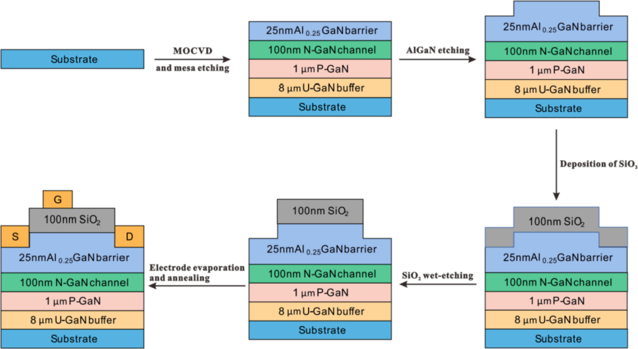
Figure 1. Fabrication processing steps of the GaN HEMTs device [9].
2.3. Heat dissipation
For now, heat dissipation has been a very important issue affecting the progress of GaN power devices. Because of the limited heat dissipation capability of the substrate and epitaxial materials, better packaging technology needs to be found to solve this problem. When the device is miniaturized, the current density is increasing and the self-heating effect of the device becomes more and more obvious, resulting in a rapid increase in the peak temperature of the device and an exponential decrease in reliability. Compared with conventional SiC substrate GaN-based power devices, diamond substrate GaN devices have higher heat dissipation capability and are expected to achieve miniaturization and high power of GaN-based power devices, thus promoting a wide range of applications in RF power devices and microwave power device-related fields. Another solution to heat dissipation is to use an embedded Manifold microchannel (MMC) heat sink. MMC is a type of microfluidic system consisting of an intricate network of miniature channels, typically in the range of tens to hundreds of micrometers in size. These systems are designed to manipulate and control small volumes of fluids, usually in the range of picoliters to microliters. The aspect ratio of the microchannels has an effect on the subcooled flow boiling in the embedded MMC heat sink of GaN HEMTs, with the lowest temperature found at microchannel aspect ratio Ʌ= 9 showed in Figure 2 [13].
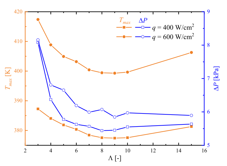
Figure 2. Maximum temperature and pressure drop as a function of micro channel aspect ratio [13].
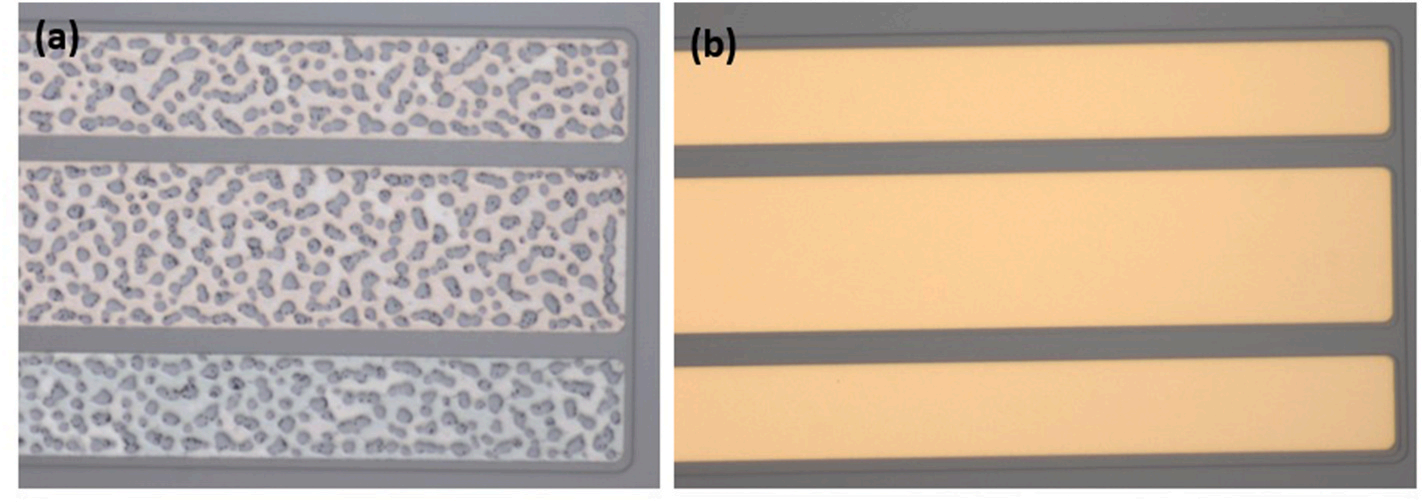
Figure 3. Pictures of alloyed (a) and nonalloyed (b) ohmic contacts for HEMT devices [14].
2.4. Performance improvements
There are some other ways to improve the performance of GaN HEMTs, such as using nonalloyed ohmic contacts. Nonalloyed ohmic contacts are typically formed by depositing a thin metal layer on the semiconductor surface, followed by a heat treatment process to improve the contact properties. The goal is to establish a low-resistance electrical path between the metal and semiconductor, which is essential for efficient device operation. Figure 3 shows alloyed and non-alloyed ohmic contacts for HEMT devices, compared to alloyed ohmic contacts, nonalloyed ohmic contacts demonstrated a decrease in contact resistance (Rc) from 0.5 ± 0.05 Ω mm to 0.34 ± 0.06 Ω mm while exhibiting improved surface morphology, furthermore, during the annealing processes with reduced device size, adverse effects on ohmic contact resistance and device performance, like purple plague effect, metal scattering, and metal leakage, were not observed in non-alloyed ohmic contact structures, particularly in HEMT devices operating in the Ka-band [14]. Another way is using the dry/wet combined etching process, which is a semiconductor manufacturing technique that combines the benefits of both dry and wet etching processes. To overcome the challenges in the integration process caused by the requirement for removal of the SiN interlayer and diamond with minimal damage, a dry and wet combined etching process can be employed to partially remove the diamond and SiN interlayer.This method ensures that the off-state current of the device with a diamond heat spreader is not degraded. Figure 4 depicts the relationship between the temperature increase and the dissipated power density (PD) for both samples, through the analysis of the device's thermal properties using electro-thermal simulation, it has been demonstrated that this process can reduce the temperature by 25 ℃ at a power density of 20W/mm [15]. Additionally, the use of an AlGaN back barrier layer and an intrinsic GaN cap layer helps avoid the problems of p-type doping and Back-to-back diode gate structure, simplifies the device fabrication process, and improves the channel constraint of two dimensional electron gas (2DEG), significantly suppressing the short-channel effect [16].
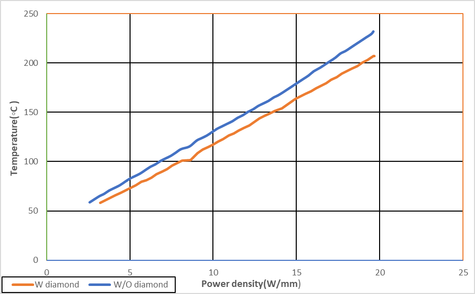
Figure 4. Relationship of the temperature and dissipated power.
3. Trend of GaN HEMT
3.1. Advancements in GaN HEMT technology
In recent years, GaN HEMT technology has continued to advance in various areas, such as crystal growth technology, sensing applications, packaging technology, and performance optimization. MOCVD technology remains one of the most commonly used crystal growth techniques, allowing for the growth of high-quality GaN epitaxial layers on various substrates. GaN HEMTs have shown great potential in gas sensors and biosensor applications due to their ability to detect various gases and biomolecules with high sensitivity and selectivity.
3.2. Trend of heat dissipation
One of the major challenges facing GaN HEMT technology is heat dissipation, which limits the miniaturization and reliability of devices. To address this issue, researchers have explored the use of diamond substrates and embedded MMC heat sinks, which have shown promising results in improving heat dissipation capabilities. Other approaches to improve device performance include the use of non-alloyed ohmic contacts, dry/wet combined etching processes, and the incorporation of an AlGaN back barrier layer and an intrinsic GaN cap layer.
3.3. Challenges and future research directions
Despite the significant advancements in GaN HEMT technology, there are still challenges that need to be addressed, such as reducing production costs and improving the yield and reliability of devices. Future research directions may focus on improving the integration of GaN HEMTs with other technologies, such as CMOS, and exploring their potential applications in emerging fields, like 5G communication. 5G will bring about changes in materials of semiconductor, as communication bands shift to higher frequencies, base stations, and communication equipment are needed to support the high-frequency performance of RF devices, GaN's advantages will gradually come to the fore, making GaN a key technology for future 5G. InGaN/GaN coupling channel HEMTs have higher drain current density, breakdown voltage, and gate voltage swing than conventional HEMTs [17], and are more suitable for 5G.
4. Conclusion
GaN HEMT technology has made significant advancements in recent years, revolutionizing the field of power electronics. Its unique properties have made it a preferred choice for various applications, including power amplifiers, power converters, and RF devices. Advancements in crystal growth technology, sensing applications, packaging technology, and performance optimization have enabled GaN HEMTs to be used in many emerging fields such as biosensing, bio-diagnostics, and genetic analysis. Heat dissipation remains a significant challenge in the miniaturization and reliability of devices, but researchers have explored several solutions, such as diamond substrates, embedded MMC heat sinks, non-alloyed ohmic contacts, and dry/wet combined etching processes. Future research directions may focus on improving the integration of GaN HEMTs with other technologies, exploring their potential applications in emerging fields, and addressing cost and yield issues.
References
[1]. Chen Yi, Han Dan, Li Donghui, HongtaoWang, He Xiuli, Liu Zhihua... & Ji Jianlong. (2023). High-performance nitrogen dioxide gas sensor for ppb-level detection based on GaN nanoshuttles. Microchemical Journal. doi:10.1016/J. MICROC. 2022.108183.
[2]. Bhat Aasif Mohammad, Poonia Ritu, Varghese Arathy, Shafi Nawaz & Periasamy C.. (2023). AlGaN/GaN high electron mobility transistor for various sensing applications: A review. Micro and Nanostructures. doi:10.1016/J. MICRNA. 2023. 207528.
[3]. .(2020). Electronics; Reports Summarize Electronics Findings from National United University (Review of GaN HEMT Applications in Power Converters over 500 W. Journal of Engineering.
[4]. Gupta Manishankar Prasad, Gorre Pradeep, Kumar Sandeep & Nulu Venugopal. (2022). A wideband, 25/40 dBm high I/O power GaN HEMT ultra-low noise amplifier using even-odd mode techniques. Microelectronics Journal. doi:10.1016/J. MEJO. 2022.105551.
[5]. E Gaubas, et al." Study of recombination characteristics in MOCVD grown GaN epi-layers on Si." Semiconductor Science and Technology 32. 12 (2017).
[6]. Hiroshi Amano. (2016). Development of GaN-based blue LEDs and metalorganic vapor phase epitaxy of GaN and related materials. Progress in Crystal Growth and Characterization of Materials (2). doi:10.1016/j. pcrysgrow. 2016.04.006.
[7]. Zhang Dongguo, Li Zhonghui, Guo Huaixin, Peng Daqing, Yang Qiankun, Li Chuanhao & Luo Weike. (2023). Research on nano-scale AlN nucleation layer growth and GaN HEMT characteristics based on MOCVD technology. Journal of Crystal Growth. p 2-6 doi:10. 1016/J. JCRYSGRO. 2023. 127155.
[8]. Liu Litao, Zhang Heqiu, Xu Ruiliang, Zhang Wenhui, Xia Xiaochuan, Hua Ruinian... & Liang Hongwei. (2023). TiO2 functionalized AlGaN/GaN HEMT gas sensor based on capacitance change strategy under room temperature. Materials Research Bulletin. p 3-5 doi:10.1016/J. MATERRESBULL. 2023.112186.
[9]. Wu Wanglong, Liu Chuankai, Han Lixiang, Wang Xiaozhou & Li Jingbo. (2023). Wafer-scale high sensitive UV photodetectors based on novel AlGaN/n-GaN/p-GaN heterostructure HEMT. Applied Surface Science. doi:10.1016/J. APSUSC.2023.156618.
[10]. Naresh Varnakavi. & Lee Nohyun. (2021). A Review on Biosensors and Recent Development of Nanostructured Materials-Enabled Biosensors. Sensors (4). doi:10.3390/S21041109.
[11]. Jia, X., Wei, J. J., Huang, Y. B., Shao, S. W., Kong, Y. C., Liu, J. L., ... & Ye, H. T. (2020). Progress in application of diamond heat spreader in GaN-based power devices. Surface Technology, 49(11), 111–123. doi:10.16490/j. cnki. issn. 1001-3660.2020.11.013.
[12]. Mouffoki Faiza, Bouguenna Driss, Dahou Fatima Zohra, Beloufa Abbès & Loan Sajad Ahmad. (2022). Performance evaluation of electrical properties of GaN MOS-HEMTs based biosensors for rapid detection of viruses. Materials Today Communications. p.6 doi:10.1016/J. MTCOMM. 2022.104726.
[13]. Tang Weiyu, Li Junye, Lu Junliang, Sheng Kuang, Wu Zan & Li Xinbao. (2023). Thermal management of GaN HEMT devices using subcooled flow boiling in an embedded manifold microchannel heat sink. Applied Thermal Engineering. doi:10.1016/J. APPLTHERMALENG. 2023.120174.
[14]. Toprak, A. and Özbay, E. (2023). Nonalloyed ohmic contact development with n+ InGaN regrowth method and analysis of its effect on AlGaN/GaN HEMT devices. Microelectronics Journal 135
[15]. Wu Mei, Wang Ping, Li Shiming, Cheng Ke, Yang Ling, Zhang Meng... & Hao Yue. (2023). Integration of polycrystalline diamond heat spreader with AlGaN/GaN HEMTs using a dry/wet combined etching process. Diamond & Related Materials. p 4 doi:10.1016/J. DIAMOND. 2023.109676.
[16]. Zhang, Cong and Yao, Ruohe. (2023). An enhancement-mode AlInN/GaN HEMTs combining intrinsic GaN cap layer and AlGaN back barrier layer. Solid State Communications 115150.
[17]. Murugapandiyan P., Kalva Sri Rama Krishna, Rajyalakshmi V., Princy B. Anni, Tarauni Yusuf U., Fletcher Augustine & Wasim Mohd. (2023). A comparative analysis of GaN and InGaN/GaN coupling channel HEMTs on silicon carbide substrate for high linear RF applications. Micro and Nanostructures. doi:10. 1016/J. MICRNA. 2023.207545.
Cite this article
Guan,W. (2023). Advancements and trends in GaN HEMT. Applied and Computational Engineering,23,245-251.
Data availability
The datasets used and/or analyzed during the current study will be available from the authors upon reasonable request.
Disclaimer/Publisher's Note
The statements, opinions and data contained in all publications are solely those of the individual author(s) and contributor(s) and not of EWA Publishing and/or the editor(s). EWA Publishing and/or the editor(s) disclaim responsibility for any injury to people or property resulting from any ideas, methods, instructions or products referred to in the content.
About volume
Volume title: Proceedings of the 2023 International Conference on Functional Materials and Civil Engineering
© 2024 by the author(s). Licensee EWA Publishing, Oxford, UK. This article is an open access article distributed under the terms and
conditions of the Creative Commons Attribution (CC BY) license. Authors who
publish this series agree to the following terms:
1. Authors retain copyright and grant the series right of first publication with the work simultaneously licensed under a Creative Commons
Attribution License that allows others to share the work with an acknowledgment of the work's authorship and initial publication in this
series.
2. Authors are able to enter into separate, additional contractual arrangements for the non-exclusive distribution of the series's published
version of the work (e.g., post it to an institutional repository or publish it in a book), with an acknowledgment of its initial
publication in this series.
3. Authors are permitted and encouraged to post their work online (e.g., in institutional repositories or on their website) prior to and
during the submission process, as it can lead to productive exchanges, as well as earlier and greater citation of published work (See
Open access policy for details).
References
[1]. Chen Yi, Han Dan, Li Donghui, HongtaoWang, He Xiuli, Liu Zhihua... & Ji Jianlong. (2023). High-performance nitrogen dioxide gas sensor for ppb-level detection based on GaN nanoshuttles. Microchemical Journal. doi:10.1016/J. MICROC. 2022.108183.
[2]. Bhat Aasif Mohammad, Poonia Ritu, Varghese Arathy, Shafi Nawaz & Periasamy C.. (2023). AlGaN/GaN high electron mobility transistor for various sensing applications: A review. Micro and Nanostructures. doi:10.1016/J. MICRNA. 2023. 207528.
[3]. .(2020). Electronics; Reports Summarize Electronics Findings from National United University (Review of GaN HEMT Applications in Power Converters over 500 W. Journal of Engineering.
[4]. Gupta Manishankar Prasad, Gorre Pradeep, Kumar Sandeep & Nulu Venugopal. (2022). A wideband, 25/40 dBm high I/O power GaN HEMT ultra-low noise amplifier using even-odd mode techniques. Microelectronics Journal. doi:10.1016/J. MEJO. 2022.105551.
[5]. E Gaubas, et al." Study of recombination characteristics in MOCVD grown GaN epi-layers on Si." Semiconductor Science and Technology 32. 12 (2017).
[6]. Hiroshi Amano. (2016). Development of GaN-based blue LEDs and metalorganic vapor phase epitaxy of GaN and related materials. Progress in Crystal Growth and Characterization of Materials (2). doi:10.1016/j. pcrysgrow. 2016.04.006.
[7]. Zhang Dongguo, Li Zhonghui, Guo Huaixin, Peng Daqing, Yang Qiankun, Li Chuanhao & Luo Weike. (2023). Research on nano-scale AlN nucleation layer growth and GaN HEMT characteristics based on MOCVD technology. Journal of Crystal Growth. p 2-6 doi:10. 1016/J. JCRYSGRO. 2023. 127155.
[8]. Liu Litao, Zhang Heqiu, Xu Ruiliang, Zhang Wenhui, Xia Xiaochuan, Hua Ruinian... & Liang Hongwei. (2023). TiO2 functionalized AlGaN/GaN HEMT gas sensor based on capacitance change strategy under room temperature. Materials Research Bulletin. p 3-5 doi:10.1016/J. MATERRESBULL. 2023.112186.
[9]. Wu Wanglong, Liu Chuankai, Han Lixiang, Wang Xiaozhou & Li Jingbo. (2023). Wafer-scale high sensitive UV photodetectors based on novel AlGaN/n-GaN/p-GaN heterostructure HEMT. Applied Surface Science. doi:10.1016/J. APSUSC.2023.156618.
[10]. Naresh Varnakavi. & Lee Nohyun. (2021). A Review on Biosensors and Recent Development of Nanostructured Materials-Enabled Biosensors. Sensors (4). doi:10.3390/S21041109.
[11]. Jia, X., Wei, J. J., Huang, Y. B., Shao, S. W., Kong, Y. C., Liu, J. L., ... & Ye, H. T. (2020). Progress in application of diamond heat spreader in GaN-based power devices. Surface Technology, 49(11), 111–123. doi:10.16490/j. cnki. issn. 1001-3660.2020.11.013.
[12]. Mouffoki Faiza, Bouguenna Driss, Dahou Fatima Zohra, Beloufa Abbès & Loan Sajad Ahmad. (2022). Performance evaluation of electrical properties of GaN MOS-HEMTs based biosensors for rapid detection of viruses. Materials Today Communications. p.6 doi:10.1016/J. MTCOMM. 2022.104726.
[13]. Tang Weiyu, Li Junye, Lu Junliang, Sheng Kuang, Wu Zan & Li Xinbao. (2023). Thermal management of GaN HEMT devices using subcooled flow boiling in an embedded manifold microchannel heat sink. Applied Thermal Engineering. doi:10.1016/J. APPLTHERMALENG. 2023.120174.
[14]. Toprak, A. and Özbay, E. (2023). Nonalloyed ohmic contact development with n+ InGaN regrowth method and analysis of its effect on AlGaN/GaN HEMT devices. Microelectronics Journal 135
[15]. Wu Mei, Wang Ping, Li Shiming, Cheng Ke, Yang Ling, Zhang Meng... & Hao Yue. (2023). Integration of polycrystalline diamond heat spreader with AlGaN/GaN HEMTs using a dry/wet combined etching process. Diamond & Related Materials. p 4 doi:10.1016/J. DIAMOND. 2023.109676.
[16]. Zhang, Cong and Yao, Ruohe. (2023). An enhancement-mode AlInN/GaN HEMTs combining intrinsic GaN cap layer and AlGaN back barrier layer. Solid State Communications 115150.
[17]. Murugapandiyan P., Kalva Sri Rama Krishna, Rajyalakshmi V., Princy B. Anni, Tarauni Yusuf U., Fletcher Augustine & Wasim Mohd. (2023). A comparative analysis of GaN and InGaN/GaN coupling channel HEMTs on silicon carbide substrate for high linear RF applications. Micro and Nanostructures. doi:10. 1016/J. MICRNA. 2023.207545.