


1. Introduction
Semiconductor devices have revolutionized modern technology, enabling high-speed data processing, efficient power management, and advanced communication systems. Wide bandgap semiconductor materials, with larger bandgaps than silicon (1.1 eV), have become research focal points due to their exceptional electronic and thermal properties that suit harsh environments.
There are two common wide bandgap materials, SiC and GaN, SiC boasts higher thermal conductivity and mechanical strength, while GaN has superior electron mobility and saturation velocity. These subtle differences result in distinct applications for each material. SiC-based devices are developed for various applications, including power electronics, RF devices, and optoelectronics [1,2] Devices based on SiC confront constraints, such as elevated manufacturing expenses and difficulties in attaining superior epitaxial growth, restricting their extensive utilization. GaN-based devices have made significant contributions to the power electronics domain and radio frequency applications [3,4]. GaN HEMTs, when compared to Si MOSFETs, demonstrate lower on-resistance and higher switching speed, resulting in less power losses and higher effectiveness. However, GaN-based devices have certain limitations such as complications with high-quality epitaxial growth, thermal management issues, and higher production costs compared to Si-based devices. Furthermore, they are more vulnerable to gate leakage currents.
Recent advances in wide bandgap semiconductor technology focus on enhancing material quality utilization and device reliability. For instance, the use of hybrid SiC-GaN structures, such as GaN-on-SiC HEMTs [5], has demonstrated improved performance. Likewise, advanced packaging techniques and thermal management strategies have enhanced reliability of wide bandgap devices. A more comprehensive model of thermal characteristics for GaN devices on different substrates has been developed, potentially guiding new GaN HEMTs thermal management strategies [6].
Wide bandgap semiconductor devices have the potential to revolutionize various electronic industries. However, their further commercialization and widespread adoption still depend on overcoming fabrication and reliability challenges.
2. Wide band gap materials
1.1. SiC properties
SiC consists of three polymorphs: 6H-SiC, 4H-SiC, & 3C-SiC, with the second variant being the favored choice for device creation. SiC offers numerous appealing traits, like a vast indirect bandgap (3.2 eV), high electric field breakdown, & remarkable thermal conductivity. In comparison to other sophisticated semiconductor materials, SiC is more easily obtainable and thoroughly investigated. These attributes render SiC appropriate for applications requiring elevated voltage, frequency, and temperature levels.
SiC-based devices are more sensitive to crystal defects and interface states than conventional Si-based devices, potentially impacting their reliability and longevity. SiC material also introduces more surface defects. Researchers have investigated the physical nature of SiC interface defects, and understanding their formation may inspire new ways to address material limitations [7].
1.2. GaN properties
GaN, a semiconductor material, belongs to the category of wide-bandgap materials. With a direct bandgap of 3.4 eV, it outperforms Si and GaAs, allowing GaN to assimilate or radiate higher energy photons. This property makes GaN suitable for optoelectronic components such as LEDs and laser diodes.
GaN has one of the highest electron mobilities among semiconductor materials. Typical mobility values range from 100 to 200 cm²/Vs. This property makes GaN suitable for high-speed electronic devices, including FETs and HEMTs where high electron mobility is crucial for achieving fast switching speeds and low power dissipation. GaN also has high thermal conductivity, helping reduce device heat emissions.
A juxtaposition of wide bandgap materials and silicon properties is shown in Table 1.
Table 1. Basic properties of different semiconductors [8].
Material | Bandgap (eV) | Mobility ( \( c{m^{2}}/V\cdot s \) ) | Permittivity | Vsat (cm/s) | Critical Field (V/cm) |
Si | 1.10 | 1400 | 11.8 | 1.0x \( {10^{7}} \) | 3.0x \( {10^{5}} \) |
GaAs | 1.42 | 8500 | 12.8 | 2.0x \( {10^{7}} \) | 4.0x \( {10^{5}} \) |
4H-SiC | 3.23 | 260 | 9.7 | 2.0x \( {10^{7}} \) | 2.9x \( {10^{5}} \) |
GaN(Bulk) | 3.40 | 900 | 9.0 | 2.5x \( {10^{7}} \) | 3.3x \( {10^{5}} \) |
GaN(HEMT) | 3.40 | 1800 | 9.0 | 2.5x \( {10^{7}} \) | 3.3x \( {10^{5}} \) |
In addition to its electrical and thermal properties, GaN also has high mechanical strength and chemical stability. Researchers [8] note that GaN's hardness and chemical stability make it challenging to polish effectively using CMP. GaN's resistance to oxidation by oxide slurry and the greater propensity for water dissociation on kinked spots than stepped spots suggest strong bonding power and low reactivity with other substances. These characteristics make GaN suitable for harsh environments.
3. Wide band gap devices
Since Infineon's introduction of the first SiC-based diode in 2001, significant strides have been made in SiC-based devices. Multiple SiC-based devices, such as MOSFETs, JFETs, and IGBTs, have demonstrated exceptional performance.
GaN-based devices include MMICs, diodes, and HEMTs. GaN's high electron mobility and saturation current density enable the production of HEMT devices for extreme condition. MMICs and diodes using GaN substrates are also utilized [9]. GaN is typically used for manufacturing high-power devices. It is also widely employed in LED, sapphire laser [10], GaN's exceptional thermal conductivity and high carrier concentration also make it suitable for power device manufacturing.
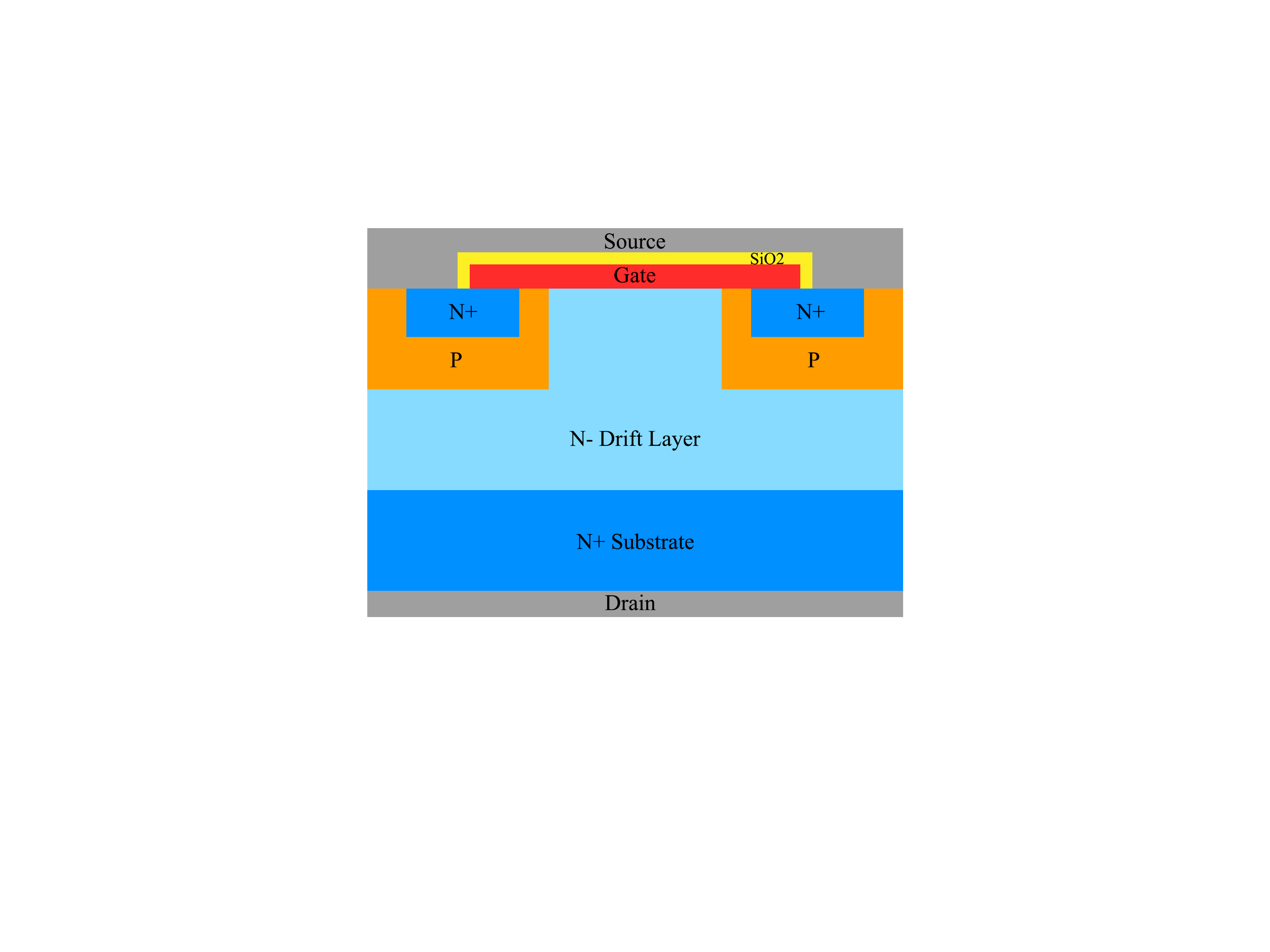
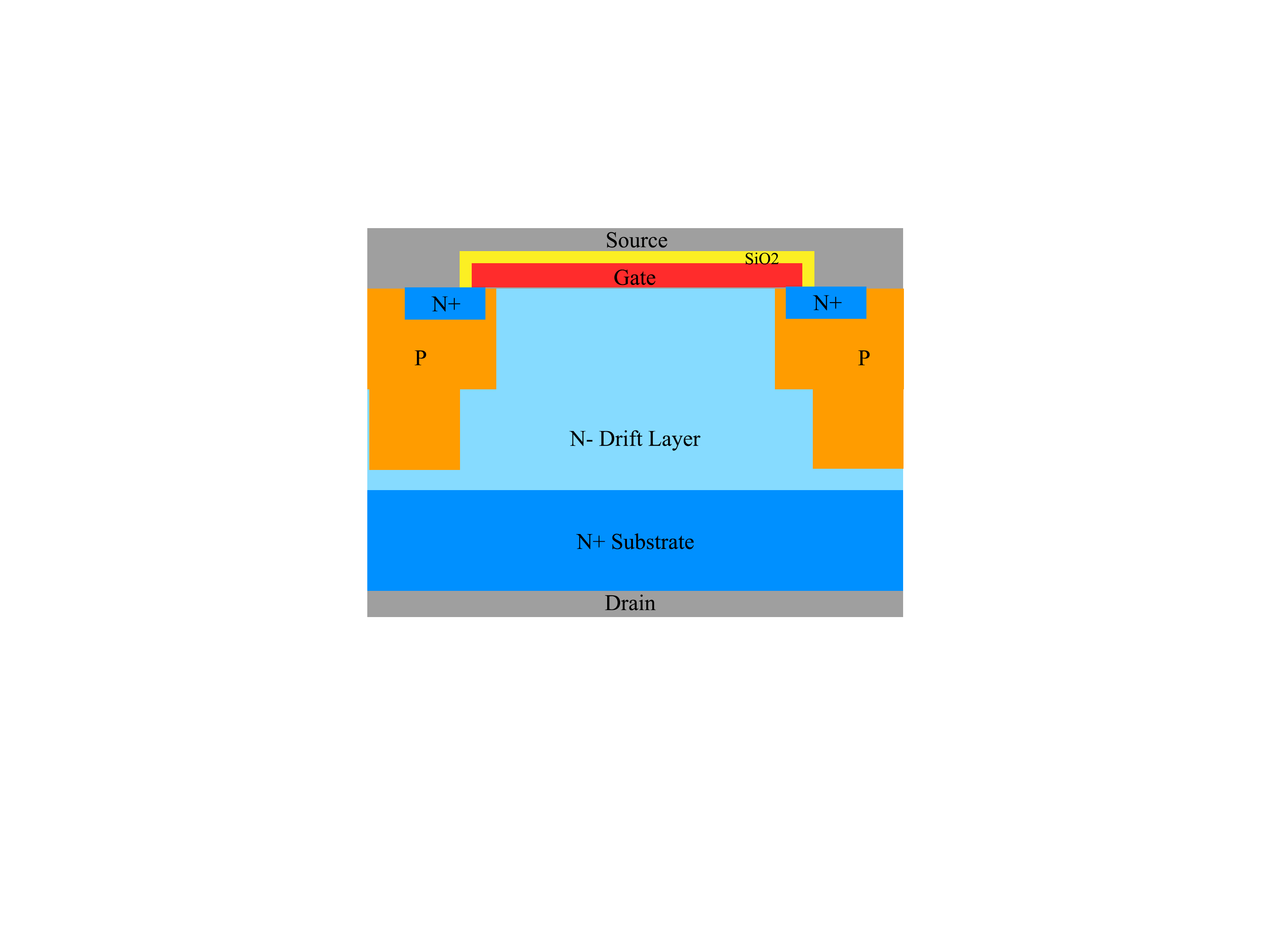
1.1. SiC based MOSFETs
MOSFET, among diverse devices, is among the most utilized power devices presently. SiC MOSFETs hold the capability to surpass Si & GaAs MOSFETs due to material benefits. SiC MOSFETs can be sorted into three classes. Their structure, merits, and demerits are illustrated in Table 2.
1.1.1. On-resistance. New structured planar SiC MOSFETs have successfully minimized the adverse effects and improved performance. Zhenfeng Peng [11] developed an HJD-MOSFET based on conventional 4H-SiC CON-DTMOSFET, achieving an \( {R_{on,sp}} \) of 2.6 \( mΩ∙{cm^{2}} \) in simulation. Zhu, S et al. used dodecagonal cell topology to decrease planar MOSFET on-resistance by 2.2x [12]. H. Yu et al. introduced an SP-structure, forming a JBS-MOSFET for better SC quality [13], reaching an on-resistance of 2.0 \( mΩ·{cm^{2}} \) .
Researchers also worked on SiC UMOSFETs to reduce electric field at trench corners and improve on-resistance. Wenchi Yang designed a deep p+ SiC UMOSFET, lowering \( {R_{on,sp}} \) to 2.04 \( mΩ·{cm^{2}} \) [14]. In 2020, Lizhi Tang designed a 1.2kV SiC trench MOSFET with optimized structural parameters [15], achieving an on-resistance of 2.35 \( mΩ·{cm^{2}} \) . Xiaojie Xu introduced JP-MOSFET in 2021 [16]. The new structure used a depletion mode P-channel MOSFET with adjustable voltage to overcome the trench breakdown. It maintained the reliability of the device and reduced \( {R_{on,sp}} \) to 1.54 \( mΩ·{cm^{2}} \) .
Table 2. Structure, advantages, and shortcomings of SiC MOSFET.
SiC MOSFET | Structure | Advantage | Shortcoming |
Planar MOSFET |
| Manufacturing process is simple. High avalanche breakdown energy. | Low channel electron mobility. JFET effect. Parasitic capacity. |
Trench MOSFET |
| Removal of JFET effect. Improved electron mobility. | Electric breakdown at the bottom of gate. |
SJ MOSFET |
| Better \( {R_{on,sp}} \) . Channel mobility is high. | Complex structure. Complicated manufacturing process. |
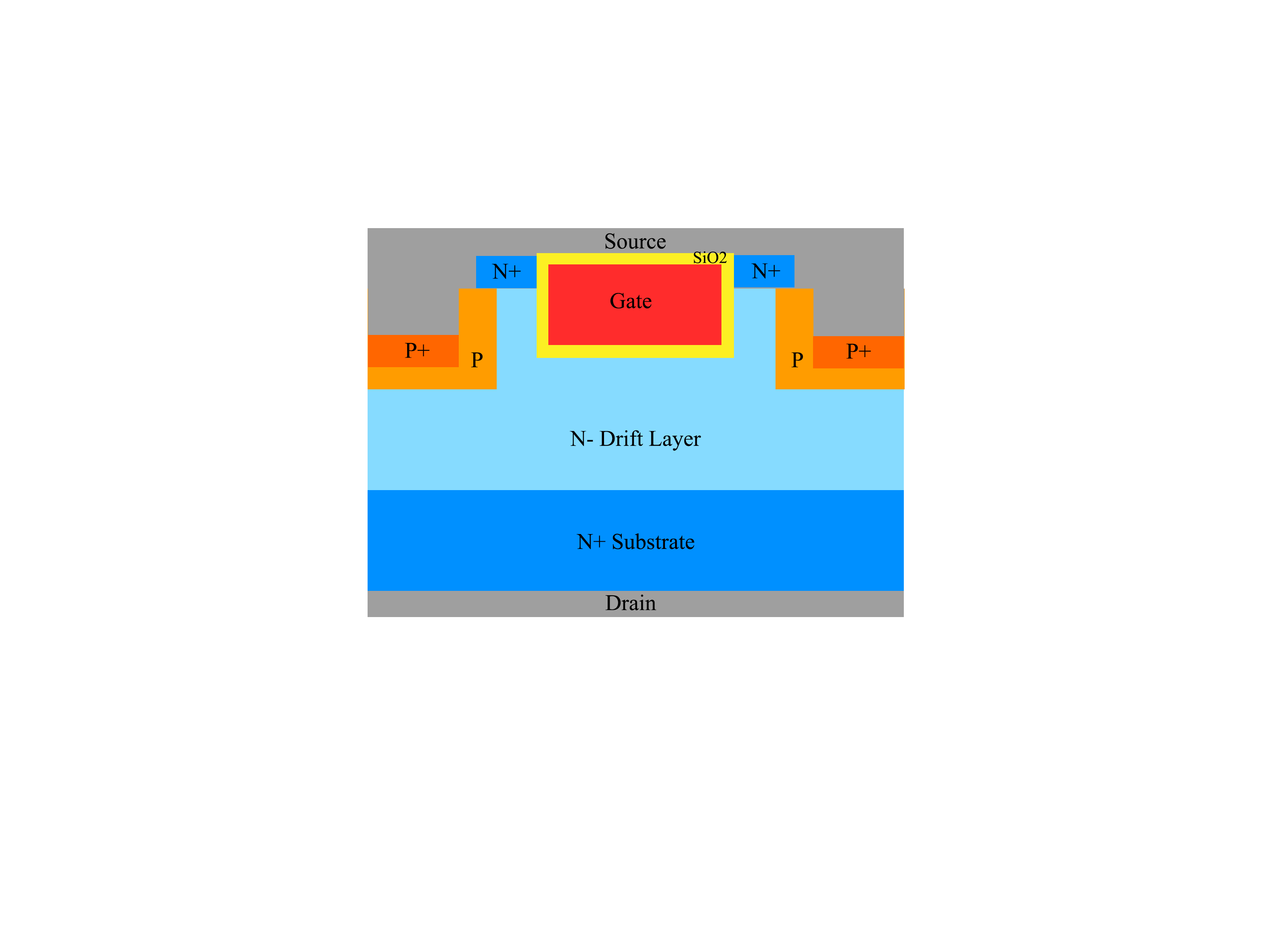
SJ MOSFETs can hold more dopant in the drift layer and offer better on-resistance. In recent years, modifying the doping process and structure has led to significant improvements. P. Vudumula and S. Kotamraju designed a SiC Super-junction MOSFET [17] with vertical dopant variation, improving on-state resistance from 13 \( mΩ·{cm^{2}} \) to 6 \( mΩ·{cm^{2}} \) . W. Cao, M. Li, Y. Ou and D. Liu came up with a dual-channel SJ MOSFET [18] and compared it with a normal dual-channel MOSFET. The SJ MOSFET shows superiorly low on-resistance at 1.09 \( mΩ·{cm^{2}} \) at room temperature. These endeavors have brought the on-resistance of SiC MOSFETs to a more advanced level.
1.1.2. electron mobility. Electron mobility in SiC MOSFETs is primarily affected by the transverse electric field, carbon clusters, and substrate doping [19]. Approaches to address this issue include nitridation, high-k material utilization, and phosphorous doping. Recent work has elevated the electron mobility of the devices.
Residual carbon clusters at the gate oxygen and interface traps result in low electron mobility. Depositing high-k materials instead of the conventional SiO2 layer has been proved effective in addressing mobility degradation. F. Arith et al. used thin SiO2 stack and a 40nm thick high-k dielectric Al2O3 layer by ALD to form a 4H-SiC MOSFET, achieving a field effect electron mobility of 125 \( {cm^{2}}/V\cdot s \) [20]. This design offers high electron mobility while maintaining minimal mobility degradation. Nitridation is another alternative for mobility improvement. A 2016 study improved SiC MOSFET mobility to 90 \( {cm^{2}}/V\cdot s \) [21]. In addition to introducing nitrides gas during oxide layer deposition, other procedures have been explored. M. Noguchi et al [22]. compared the mobility in the reversion layer of a nitride SiC MOSFET and a phosphorus-doped one. The peak mobility results were 22 \( {cm^{2}}/V\cdot s \) . for nitridation and 87 \( {cm^{2}}/V\cdot s \) . for phosphorus doping. Therefore, phosphorus doping can also be a viable method for improving electron mobility. The researchers concluded that reducing Coulomb scattering may be a hopeful solution to the channel mobility problem.
1.1.3. Temperature dependency. SiC MOSFETs are known for their ability to withstand high temperatures. Investigating how their properties change with temperature is crucial for developing accurate thermal models and maximizing the temperature-tolerance of these devices.
On-resistance increases with temperature within a certain range. Research has shown a positive correlation between on-resistance and junction temperature from 350K to 77K due to an increase in carrier concentration [23]. The thermal property of drain current is more complex. Saturation current and mobility initially increase with temperature and then decrease [8,24]. This occurrence can be ascribed to the release of electrons from energy levels of traps and a shift in the principal scattering mechanism. In addition, as the temperature increases, the threshold voltage of SiC MOSFETs decreases [25].
1.2. SiC JFET
1.1.4. Structure and recent development. A JFET is a semiconductor device with three terminals, including a source, drain, and gate, which controls current flow by modulating the conductivity of a narrow semiconductor channel. The gate is crafted using a semiconductor material featuring a reverse doping type in comparison to the channel, and voltage application to the gate creates a depletion zone around the pn-junction linking the gate and channel. Consequently, this diminishes the quantity of free charge carriers within the channel, leading to a decline in current flow from the source to drain terminals.
1.1.5. Recent studies on properties of SiC JFET. SiC JFETs exhibit high electron mobility which enables faster switching speeds and improved overall performance. High electron mobility allows SiC JFETs to operate efficiently at high frequencies and maintain low \( {R_{on}} \) .
The on-resistance ( \( {R_{on}} \) ) can be affected by JFET width ( \( {W_{J}} \) ), JFET doping ( \( {N_{J}} \) ), and cell pitch ( \( P \) ). Narrower JFETs and lower doping result in higher resistance in vertical current flow, increasing on-resistance. Tighter cell pitch reduces on-resistance by increasing the number of parallel current paths in the horizontal direction. \( {R_{on,sp}} \) is used to quantify performance, where a lower \( {R_{on,sp}} \) indicates better performance. A study has achieved a record-low \( {R_{on,sp}} \) of 2.06 \( mΩ·c{m^{2}} \) for 650 V SiC JFETs with optimized region design, highlighting their potential for superior performance and efficiency in power electronics applications [26,27].
As temperature increases, drain current also increases due to rise in channel mobility and decrease in threshold voltage, while transconductance decreases because of the reduction in gate-to-channel capacitance and increase in channel resistance. With temperature elevation, GaN's on-state resistance and forward voltage drop incline, attributable to the decrease in carrier concentration and the growth in contact resistance. In contrast, the reverse recovery charge and duration lessen due to the contracted minority carrier lifetime and diffusion length. There is no relation between \( {V_{BD}} \) (breakdown voltage) and temperature due to SiC's high bandgap and low intrinsic carrier concentration. The leakage current is also independent of temperature for the same reason. Capacitance between gate and drain and Miller charge decrease with temperature because of the reduction in depletion layer width and electric field [28].
1.3. SiC IGBT
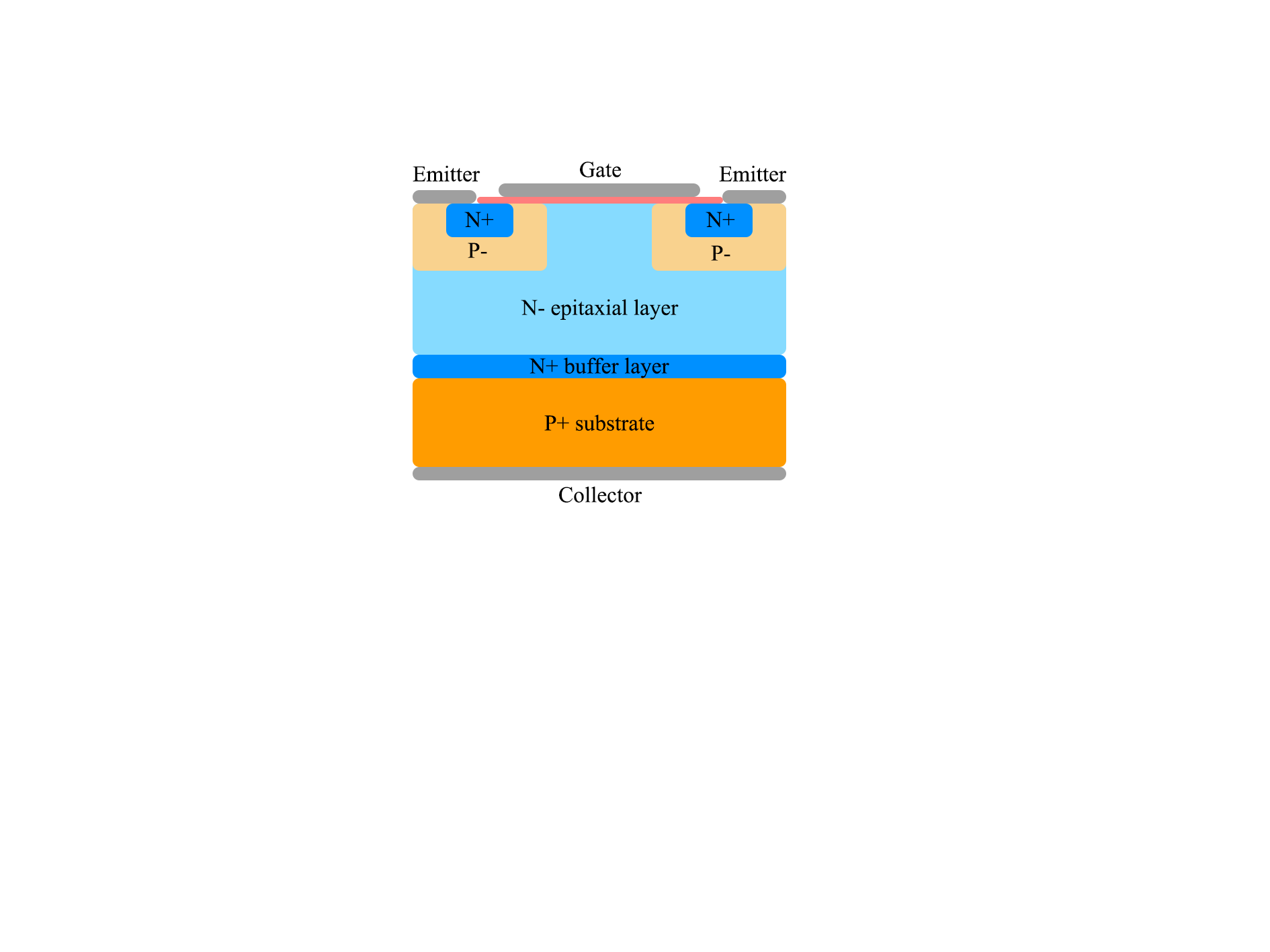
Figure 1. Structure of SiC IGBT.
1.1.6. Structure and recent development. SiC Insulated Gate Bipolar Transistor (IGBT) has a special structure innovated by SiC MOSFET and BJT. Its structure is shown in Figure 1. It integrates the advantages of both devices. Due to poor quality of p-type substrate SiC material, p-channel IGBT is better developed. As a relatively new and almost all-around device, SiC IGBT shows great prospect in high-power application.
1.1.7. Recent studies on properties of SiC IGBT. The conductivity modulation effect and CSL in SiC IGBT can aid in augmenting the device's electron mobility. For enhanced conduction properties, electron mobility is a crucial aspect for researchers to concentrate on. Carbon clusters' interference, fixed charges on the SiO2/SiC interface, and ion implantation result in unsatisfactory electron mobility. Additionally, n-channel SiC IGBT is deemed more promising compared to the p-channel variant due to the superior electron mobility in n-type SiC substrate. Although, however, there has been little research presenting specific statistics of electron mobility improvement in recent years, the advance of on-resistance can reflect the progress of electron mobility to some degree.
The on-resistance of a SiC IGBT is far beyond the limit of SiC MOSFET thanks to conductivity modulation effect in drifting region. With the introduction of CSL, the on-resistance is further reduced. In recent years, by improving the layout and structure of IGBT, on-resistance continues being improved.
In 2019, Zheng-Xin Wen et al. deigned a SiC IGBT in a hexagonal-cell layout with a differential \( {R_{on,sp}} \) of 56.92 \( mΩ∙{cm^{2}} \) [29]. The new structure demonstrated 21.3% improvement of on-resistance comparing with the conventional layout. More recent research using box cell layout by Naoki Watanabe et al. in 2022 successfully reduced the specific differential on-resistance to 13 \( mΩ∙{cm^{2}} \) . [30] These improvements indicate the effective role of cell layout in optimizing the conduction performance of SiC IGBT. Innovation of channel structure can also modify on-resistance. Xiao-Chuan Deng et al. in 2022 published a hybrid-channel injection enhanced modulation IGBT and showed improvement of \( {R_{on,sp}} \) as well [31].
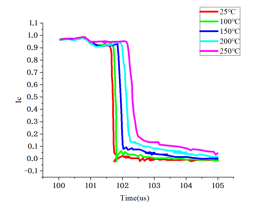
Figure 2. Switching current of a SiC IGBT under different temperature.
The influence of temperature on conduction characteristics and voltage endurance of SiC IGBT is crucial since the ideal application environment of SiC IGBT is under harsh condition. The carrier mobility of SiC is positively dependent with temperature, resulting in a similar trend of temperature dependency of SiC IGBT on-state characteristics. The output current increases as temperature rises. Switching performance of SiC IGBT also has a close relationship with temperature. It has been investigated by Kai Matsuura et al. that the main factor of highly temperature dependent switching performance is the SiO2/SiC interface trap density [32]. The switching performance (I-V characteristic) of a SiC IGBT at a range of temperature is shown in figure 2.
SiC IGBT is a relatively new device. Although there have been certain improvements of its properties, the potential of it is not sufficiently discovered yet. As a device combining advantages of MOSFET and BJT, it has potentiality to be a better alternative than other existing devices in the future. Therefore, the device still requires further exploration.
1.4. GaN HEMT
1.1.8. On Resistance. Dynamic on-resistance ( \( {dR_{on}} \) ) impacts GaN HEMTs' performance and reliability, with trapped charge causing unpredictable conduction loss. Researchers [33] found that interface and surface traps are primary \( {dR_{on}} \) contributors, with temperature-independent tunneling and thermally activated electron de-trapping processes as the main mechanisms. To reduce \( {dR_{on}} \) and enhance performance, they recommend controlling trap numbers by increasing buffer thickness, reducing gate length, using heterogeneous structures, and new materials [34].
1.1.9. Mobility. The mobility of electrons in GaN is usually higher than that of holes because of material quality, doping concentration and temperature. GaN's high mobility allows it to develop efficient and reliable high-speed electronic devices.
Due to its high electron mobility, GaN has become a compelling substitute. The presence of two-dimensional electron gas (2DEG) at the GaN and AlGaN interface leads its electron mobility to a rather high level. Proper control of 2DEG interactions can optimize GaN-based device’s performance. Despite its high channel mobility and high breakdown voltage, GaN MOSFET suffers from lower interface quality and higher interface trap density than silicon MOSFET, which degrades electron mobility due to Coulomb scattering [35]. Meanwhile, GaN MOSFET can achieve normally-off operation without current collapse problems by using suitable gate dielectrics and mobility enhancement layers [36].
1.1.10. Temperature Dependence. An important consideration when using GaN in electronic devices is its temperature dependence.
The temperature dependence of GaN is evident in the fluctuation of its electrical, optical, and mechanical features. The electron mobility, one of the most crucial parameters, is affected by temperature. The electron mobility in GaN has an inverse relationship with temperature, and research [37]has revealed that the mixed influence from increase and degeneration of phonons as temperature rises comprehensively result in the negative temperature dependency.
The temperature dependence of GaN also affects its electrical performance. The conductivity of GaN increases with temperature due to the increased ionization of impurities and defects, which produces free carriers. Researchers [38] also found that the high-temperature p-GaN HEMT devices threshold voltage fluctuations are minor and mainly impacted by GaN's bandgap and interface states or obstacles. The decline in transconductance and rise in on-resistance primarily originate from the reduction in carrier mobility. The rise in drain current might result from the decline in barriers' trap and the surge in intrinsic carrier concentration.
To mitigate the effects of temperature on GaN-based devices, researchers explored various strategies. For example, researchers [39] are etching microgrooves on the substrate and filling them with high thermal conductivity material copper to improve the device’s thermal performance. The investigators established that using current-voltage traits, pulse experiments, and Raman thermometry techniques, this configuration could effectively mitigate the device's self-heating impact, amplify the saturated drain current and transconductance, and prolong the device's longevity.
4. Comparison and evaluation between SiC and GaN devices
SiC and GaN devices both have lower on-resistance than traditional silicon-based ones. However, SiC MOSFETs typically have lower on-resistance than GaN HEMTs due to their higher electron mobility.
As mentioned earlier, a 1200 V SiC planar MOSFET designed by Zhenfeng Peng has a \( {R_{on,sp}} \) of 2.6 \( mΩ∙{cm^{2}} \) at a drain current density of 100 A/cm2 [11]. In comparison, a 650V GaN HEMT designed by Wenzhong Lu and colleagues has \( {R_{on,sp}} \) of 4.7 \( mΩ∙{cm^{2}} \) at a drain current density of 50A/cm2.
Similarly, in the research by Xiaojie Xu mentioned earlier, a new trench SiC MOSFET structure called JP-MOSFET was proposed [14], which achieved an \( {R_{on,sp}} \) of 1.54 \( mΩ∙{cm^{2}} \) . In comparison, a 650V GaN HEMT designed by Jian Zhang and colleagues has an \( {R_{on,sp}} \) of 2.16 \( mΩ∙{cm^{2}} \) , which is quite similar to the Ron, sp of SiC JP-MOSFET in Xu's work, at a drain current density of 50 A/cm2.
These examples suggest that SiC MOSFETs generally have a lower on-resistance than GaN HEMTs at comparable voltage and current levels. However, it's worth noting that both SiC and GaN devices have been improved significantly in recent years. They have both achieved extremely low on-resistance, indicating a promising future for building ideal electron devices and getting better output qualities. \( {R_{on,sp}} \) can vary widely depending on the specific device design and manufacturing process.
SiC has a high electron mobility of up to 2000 cm²/Vs at room temperature, which is significantly higher than that of GaN. GaN typically has an electron mobility of around 1000 cm²/Vs at room temperature, though it can be improved through doping, strain engineering, and device structure optimization. The high electron mobility of SiC is one of the key factors that can lead to more efficient and compact devices.
GaN also has some advantages in terms of electron mobility. For example, it has a higher saturation velocity than SiC. It can sustain higher electric fields and achieve higher output power. Additionally, GaN has a wider bandgap than SiC. This can reduce the impact of parasitic capacitances and improve device performance at high frequencies.
While there has been plenty of study to improve the electron mobility of the two materials, the solutions may head toward different directions. SiC has more problems to do with the interference from carbon and trap electronic energy levels, which is more correlative with the material properties. GaN is limited by the two-dimensional electron layer at the interface between GaN and AlGaN layers, which is, in fact, a result of the interaction between the two layers. This comparison provides a clearer picture of essence of mobility of SiC and GaN, it also implies difference in physical and chemical structures of the two materials.
Overall, while SiC has a higher electron mobility than GaN, GaN is better in other qualities like frequency property. Which one should be used in certain application depends on the specific application demands.
SiC and GaN have different temperature dependence characteristics. SiC has a smaller negative temperature coefficient of resistance (TCR) compared to GaN. This is due to SiC's wider bandgap and higher thermal conductivity. As temperature increases, the mobility of charge carriers decreases, then the conductivity drops and an increase appears in on-resistance for both SiC and GaN devices.
However, the severer temperature dependence of GaN can limit their performance in high-temperature applications. GaN devices typically have a higher TCR and lower thermal conductivity, which can lead to self-heating and temperature-dependent device characteristics. This means that GaN devices may require additional thermal management solutions to maintain their performance at high temperatures.
In contrast, SiC devices have a more stable performance over a wider temperature range due to their lower TCR and higher thermal conductivity. SiC devices maintain high performance quality under extreme condition. Therefore, they are ideal for high-temperature use such as power electronics in electric vehicles and aerospace systems.
Overall, comparing with GaN devices, SiC devices have a more favorable temperature coefficient of resistance and thermal conductivity. GaN devices have more high-frequency application, whereas SiC is applied more at high temperature and high voltage for its steadiness and favorable thermal qualities.
5. Conclusion
SiC and GaN are two wide bandgap semiconductor materials that have unique electronic and thermal properties that make them suitable for harsh environments. SiC-based devices have been developed for applications including power electronic facilities, RF devices, and optoelectronics. Many types of SiC power devices have been developed and they are providing a hopeful picture of an electronic system with lower power losses and higher efficiency compared to conventional Si-based devices. Similarly, GaN-based devices have also been developed for power electronics and RF applications. GaN HEMTs have emerged as a promising alternative to conventional Si MOSFETs. GaN HEMTs have better conduction characteristic and higher switching speed compared to Si MOSFETs, which results in lower power losses and higher efficiency. With recent advances in wide bandgap semiconductor technology focused on improving material quality and increasing device reliability, these devices have the potential to revolutionize a range of industries, including power electronics, RF applications, and optoelectronics.
References
[1]. Han L., Liang L., Kang Y., Qiu Y., 2021, A Review of SiC IGBT: Models, Fabrications, Characteristics, and Applications, IEEE Transactions on Power Electronics 36(2) 2080-2093.
[2]. Chaujar R., 2019, Analog and RF assessment of sub-20 nm 4H-SiC trench gate MOSFET for high frequency applications, AEU - International Journal of Electronics and Communications 98 51-57.
[3]. Pushpakaran B. N., Subburaj A. S., Bayne S. B., 2020, Commercial GaN-Based Power Electronic Systems: A Review, Journal of Electronic Materials 49(11) 6247-6262.
[4]. Zhang Y., Zubair A., Liu Z., Xiao M., Perozek J., Ma Y., Palacios T., 2021, GaN FinFETs and trigate devices for power and RF applications: Review and perspective, Semiconductor Science and Technology 36(5) 054001.
[5]. Duffy M. R., Lasser G., Nevett G., Roberg M., Popović Z., 2019, A three-stage 18.5–24-GHz GaN-on-SiC 4 W 40% efficient MMIC PA, IEEE Journal of Solid-State Circuits 54(9) 2402-2410.
[6]. El-Helou A., Cui Y., Tadjer M., Anderson T., Francis D., Feygelson T., Pate B., Hobart K., Raad P., 2020, Full thermal characterization of AlGaN/GaN high electron mobility transistors on silicon, silicon carbide, and diamond substrates using a reverse modeling approach, Semiconductor Science and Technology 36(1) 014008.
[7]. Fisicaro G., Bongiorno C., Deretzis I., Giannazzo F., Via F. L., Roccaforte F., Zielinski M., Zimbone M., Magna A. L., 2020, Genesis and evolution of extended defects: The role of evolving interface instabilities in cubic SiC, Applied Physics Reviews 7(2) 021402.
[8]. Kawaguchi K., Wang Y., Xu J., Ootani Y., Higuchi Y., Ozawa N., Kubo M., 2021, Cooperative roles of chemical reactions and mechanical friction in chemical mechanical polishing of gallium nitride assisted by OH radicals: tight-binding quantum chemical molecular dynamics simulations, Physical Chemistry Chemical Physics 23(7) 4075-4084.
[9]. Pu T., Younis U., Chiu H.-C., Xu K., Kuo H.-C., Liu X., 2021, Review of Recent Progress on Vertical GaN-Based PN Diodes, Nanoscale Research Letters 16(1) 101.
[10]. Tian W., Wu Y., Wu T., Dou L., Cao X., Li J., 2022, Mechanisms and Performance Analysis of GaN-Based Micro-LED Grown on Pattern Sapphire Substrate by Laser Lift-Off Process, ECS Journal of Solid State Science and Technology 11(4) 046001.
[11]. Peng Z., 2021, Design and experimental study of 1200V 4H-SiC planar MOSFET, University of Electronic Science and Technology.
[12]. Zhu S., Liu T., Fan J., Salemi A., White M. H., Sheridan D., Agarwal A. K., 2022, A New Cell Topology for 4H-SiC Planar Power MOSFETs for High-Frequency Switching, Materials 15(19) 6690.
[13]. Yu H., Wang J., Deng G., Liang S., Liu H., Shen Z. J., 2022, A Novel 4H-SiC JBS-Integrated MOSFET With Self-Pinching Structure for Improved Short-Circuit Capability, IEEE Transactions on Electron Devices 69(9) 5104-5109.
[14]. Xu X., 2021, Study on novel structures for 1.2kV SiC MOSFETs, University of Electronic Science and Technology.
[15]. Tang L., 2020, Design of 1.2kV trench SiC power MOSFET, Southeast University.
[16]. Yang W., 2019, New structure design and characteristics research of SiC UMOSFET, University of Electronic Science and Technology.
[17]. Vudumula P., Kotamraju S., 2019, Design and Optimization of SiC Super-Junction MOSFET Using Vertical Variation Doping Profile, IEEE Transactions on Electron Devices 66(3) 1402-1408.
[18]. Cao W., Li M., Ou Y., Liu D., 2022, 1.2-kV SiC Superjunction Dual-channel MOSFET with Ultra Low Specific on-Resistance, 2022 IEEE 17th Conference on Industrial Electronics and Applications (ICIEA), pp. 64-68.
[19]. Das S., Zheng Y., Ahyi A., Kuroda M. A., Dhar S., 2022, Study of Carrier Mobilities in 4H-SiC MOSFETS Using Hall Analysis, Materials 15(19) 6736.
[20]. Arith F., Urresti J., Vasilevskiy K., Olsen S., Wright N., O’Neill A., 2018, Increased Mobility in Enhancement Mode 4H-SiC MOSFET Using a Thin SiO2 / Al2O3 Gate Stack, IEEE Electron Device Letters 39(4) 564-567.
[21]. Li F., Sharma Y. K., Jennings M. R., Pérez-Tomás A., Shah V. A., Rong H., Russell S., Martin D. M., Mawby P. A., 2016, Improved Channel Mobility by Oxide Nitridation for N-Channel MOSFET on 3C-SiC(100)/Si, Materials Science Forum 858 667-670.
[22]. Noguchi M., Watanabe T., Watanabe H., Kita K., Miura N., 2021, Comparative Study of Hall Effect Mobility in Inversion Layer of 4H-SiC MOSFETs With Nitrided and Phosphorus-Doped Gate Oxides, IEEE Transactions on Electron Devices 68(12) 6321-6329.
[23]. Hong K., Chen X. Y., Chen Y., Zhang M. S., Wang J. L., Jiang S., Pang Z., Yang H. M., Xue N., Gou H. Y., Zeng L., 2019, Experimental Investigations Into Temperature and Current Dependent On-State Resistance Behaviors of 1.2 kV SiC MOSFETs, IEEE Journal of the Electron Devices Society 7 925-930.
[24]. Sun J., Xu H., Wu X., Yang S., Guo Q., Sheng K., 2017, Short circuit capability and high temperature channel mobility of SiC MOSFETs, 2017 29th International Symposium on Power Semiconductor Devices and IC's (ISPSD), pp. 399-402.
[25]. Moscatelli F., Poggi A., Solmi S., Nipoti R., 2008, Nitrogen Implantation to Improve Electron Channel Mobility in 4H-SiC MOSFET, IEEE Transactions on Electron Devices 55(4) 961-967.
[26]. Liu T., Zhu S., Salemi A., Sheridan D., White M. H., Agarwal A. K., 2021, JFET Region Design Trade-Offs of 650 V 4H-SiC Planar Power MOSFETs, Solid State Electronics Letters 3 53-58.
[27]. Shrestha N., Mazumder S. K., Voss L., 2021, Electrical Properties of Optically Triggered SiC JFET for Power Electronic Application, 2021 IEEE 12th International Symposium on Power Electronics for Distributed Generation Systems (PEDG), pp. 1-6.
[28]. Funaki T., Kashyap A. S., Mantooth H. A., Balda J. C., Barlow F. D., Kimoto T., Hikihara T., 2006, Characterization of SiC JFET for temperature dependent device modeling, 2006 37th IEEE Power Electronics Specialists Conference, pp. 1-6.
[29]. Wen Z.-X., Zhang F., Shen Z.-W., Chen J., He Y.-W., Yan G.-G., Liu X.-F., Zhao W.-S., Wang L., Sun G.-S., Zeng Y.-P., 2019, Design and fabrication of 10-kV silicon–carbide p-channel IGBTs with hexagonal cells and step space modulated junction termination extension*, Chinese Physics B 28(6) 068504.
[30]. Watanabe N., Okino H., Shima A., 2022, Impact of Cell Layout on On-state and Dynamic Characteristics of N-channel SiC IGBTs, 2022 IEEE 34th International Symposium on Power Semiconductor Devices and ICs (ISPSD), pp. 85-88.
[31]. Deng X., Cheng Z., Chen Z., Wu H., Bai S., Li X., Li X., Chen W., Zhang B., 2022, A Hybrid-Channel Injection Enhanced Modulation 4H-SiC IGBT Transistors With Improved Performance, IEEE Transactions on Electron Devices 69(8) 4421-4426.
[32]. Matsuura K., Tanimoto Y., Saito A., Miyaoku Y., Mizoguchi T., Miura-Mattausch M., Mattausch H. J., 2019, Analysis and compact modeling of temperature-dependent switching in SiC IGBT circuits, Solid-State Electronics 153 59-66.
[33]. Mishra U. K., Parikh P., Wu Y.-F., 2002, AlGaN/GaN HEMTs-an overview of device operation and applications, Proceedings of the IEEE 90(6) 1022-1031.
[34]. Sequeira M. C., Mattei J.-G., Vazquez H., Djurabekova F., Nordlund K., Monnet I., Mota-Santiago P., Kluth P., Grygiel C., Zhang S., Alves E., Lorenz K., 2021, Unravelling the secrets of the resistance of GaN to strongly ionising radiation, Communications Physics 4(1) 51.
[35]. Pérez-Tomás A., Fontserè A., 2011, AlGaN/GaN hybrid MOS-HEMT analytical mobility model, Solid-State Electronics 56(1) 201-206.
[36]. Smith M., Kajiwara Y., Ono H., Huang P. C., Kato D., Mukai A., Shindome A., Kuraguchi M., 2021, High mobility in GaN MOSFETs with AlSiO gate dielectric and AlN mobility enhancement layer, 2021 IEEE 8th Workshop on Wide Bandgap Power Devices and Applications (WiPDA), pp. 283-287.
[37]. Poncé S., Jena D., Giustino F., 2019, Hole mobility of strained GaN from first principles, Physical Review B 100(8) 085204.
[38]. Li S., Liu S., Tian Y., Zhang C., Wei J., Tao X., Li N., Zhang L., Sun W., 2020, High-temperature electrical performances and physics-based analysis of p-GaN HEMT device, IET Power Electronics 13(3) 420-425.
[39]. Mohanty S. K., Chen Y.-Y., Yeh P.-H., Horng R.-H., 2019, Thermal Management of GaN-on-Si High Electron Mobility Transistor by Copper Filled Micro-Trench Structure, Scientific Reports 9(1) 19691.
Cite this article
Zhang,M.;Zhang,Y. (2023). Status and prospects of wide bandgap semiconductor devices. Applied and Computational Engineering,23,252-262.
Data availability
The datasets used and/or analyzed during the current study will be available from the authors upon reasonable request.
Disclaimer/Publisher's Note
The statements, opinions and data contained in all publications are solely those of the individual author(s) and contributor(s) and not of EWA Publishing and/or the editor(s). EWA Publishing and/or the editor(s) disclaim responsibility for any injury to people or property resulting from any ideas, methods, instructions or products referred to in the content.
About volume
Volume title: Proceedings of the 2023 International Conference on Functional Materials and Civil Engineering
© 2024 by the author(s). Licensee EWA Publishing, Oxford, UK. This article is an open access article distributed under the terms and
conditions of the Creative Commons Attribution (CC BY) license. Authors who
publish this series agree to the following terms:
1. Authors retain copyright and grant the series right of first publication with the work simultaneously licensed under a Creative Commons
Attribution License that allows others to share the work with an acknowledgment of the work's authorship and initial publication in this
series.
2. Authors are able to enter into separate, additional contractual arrangements for the non-exclusive distribution of the series's published
version of the work (e.g., post it to an institutional repository or publish it in a book), with an acknowledgment of its initial
publication in this series.
3. Authors are permitted and encouraged to post their work online (e.g., in institutional repositories or on their website) prior to and
during the submission process, as it can lead to productive exchanges, as well as earlier and greater citation of published work (See
Open access policy for details).
References
[1]. Han L., Liang L., Kang Y., Qiu Y., 2021, A Review of SiC IGBT: Models, Fabrications, Characteristics, and Applications, IEEE Transactions on Power Electronics 36(2) 2080-2093.
[2]. Chaujar R., 2019, Analog and RF assessment of sub-20 nm 4H-SiC trench gate MOSFET for high frequency applications, AEU - International Journal of Electronics and Communications 98 51-57.
[3]. Pushpakaran B. N., Subburaj A. S., Bayne S. B., 2020, Commercial GaN-Based Power Electronic Systems: A Review, Journal of Electronic Materials 49(11) 6247-6262.
[4]. Zhang Y., Zubair A., Liu Z., Xiao M., Perozek J., Ma Y., Palacios T., 2021, GaN FinFETs and trigate devices for power and RF applications: Review and perspective, Semiconductor Science and Technology 36(5) 054001.
[5]. Duffy M. R., Lasser G., Nevett G., Roberg M., Popović Z., 2019, A three-stage 18.5–24-GHz GaN-on-SiC 4 W 40% efficient MMIC PA, IEEE Journal of Solid-State Circuits 54(9) 2402-2410.
[6]. El-Helou A., Cui Y., Tadjer M., Anderson T., Francis D., Feygelson T., Pate B., Hobart K., Raad P., 2020, Full thermal characterization of AlGaN/GaN high electron mobility transistors on silicon, silicon carbide, and diamond substrates using a reverse modeling approach, Semiconductor Science and Technology 36(1) 014008.
[7]. Fisicaro G., Bongiorno C., Deretzis I., Giannazzo F., Via F. L., Roccaforte F., Zielinski M., Zimbone M., Magna A. L., 2020, Genesis and evolution of extended defects: The role of evolving interface instabilities in cubic SiC, Applied Physics Reviews 7(2) 021402.
[8]. Kawaguchi K., Wang Y., Xu J., Ootani Y., Higuchi Y., Ozawa N., Kubo M., 2021, Cooperative roles of chemical reactions and mechanical friction in chemical mechanical polishing of gallium nitride assisted by OH radicals: tight-binding quantum chemical molecular dynamics simulations, Physical Chemistry Chemical Physics 23(7) 4075-4084.
[9]. Pu T., Younis U., Chiu H.-C., Xu K., Kuo H.-C., Liu X., 2021, Review of Recent Progress on Vertical GaN-Based PN Diodes, Nanoscale Research Letters 16(1) 101.
[10]. Tian W., Wu Y., Wu T., Dou L., Cao X., Li J., 2022, Mechanisms and Performance Analysis of GaN-Based Micro-LED Grown on Pattern Sapphire Substrate by Laser Lift-Off Process, ECS Journal of Solid State Science and Technology 11(4) 046001.
[11]. Peng Z., 2021, Design and experimental study of 1200V 4H-SiC planar MOSFET, University of Electronic Science and Technology.
[12]. Zhu S., Liu T., Fan J., Salemi A., White M. H., Sheridan D., Agarwal A. K., 2022, A New Cell Topology for 4H-SiC Planar Power MOSFETs for High-Frequency Switching, Materials 15(19) 6690.
[13]. Yu H., Wang J., Deng G., Liang S., Liu H., Shen Z. J., 2022, A Novel 4H-SiC JBS-Integrated MOSFET With Self-Pinching Structure for Improved Short-Circuit Capability, IEEE Transactions on Electron Devices 69(9) 5104-5109.
[14]. Xu X., 2021, Study on novel structures for 1.2kV SiC MOSFETs, University of Electronic Science and Technology.
[15]. Tang L., 2020, Design of 1.2kV trench SiC power MOSFET, Southeast University.
[16]. Yang W., 2019, New structure design and characteristics research of SiC UMOSFET, University of Electronic Science and Technology.
[17]. Vudumula P., Kotamraju S., 2019, Design and Optimization of SiC Super-Junction MOSFET Using Vertical Variation Doping Profile, IEEE Transactions on Electron Devices 66(3) 1402-1408.
[18]. Cao W., Li M., Ou Y., Liu D., 2022, 1.2-kV SiC Superjunction Dual-channel MOSFET with Ultra Low Specific on-Resistance, 2022 IEEE 17th Conference on Industrial Electronics and Applications (ICIEA), pp. 64-68.
[19]. Das S., Zheng Y., Ahyi A., Kuroda M. A., Dhar S., 2022, Study of Carrier Mobilities in 4H-SiC MOSFETS Using Hall Analysis, Materials 15(19) 6736.
[20]. Arith F., Urresti J., Vasilevskiy K., Olsen S., Wright N., O’Neill A., 2018, Increased Mobility in Enhancement Mode 4H-SiC MOSFET Using a Thin SiO2 / Al2O3 Gate Stack, IEEE Electron Device Letters 39(4) 564-567.
[21]. Li F., Sharma Y. K., Jennings M. R., Pérez-Tomás A., Shah V. A., Rong H., Russell S., Martin D. M., Mawby P. A., 2016, Improved Channel Mobility by Oxide Nitridation for N-Channel MOSFET on 3C-SiC(100)/Si, Materials Science Forum 858 667-670.
[22]. Noguchi M., Watanabe T., Watanabe H., Kita K., Miura N., 2021, Comparative Study of Hall Effect Mobility in Inversion Layer of 4H-SiC MOSFETs With Nitrided and Phosphorus-Doped Gate Oxides, IEEE Transactions on Electron Devices 68(12) 6321-6329.
[23]. Hong K., Chen X. Y., Chen Y., Zhang M. S., Wang J. L., Jiang S., Pang Z., Yang H. M., Xue N., Gou H. Y., Zeng L., 2019, Experimental Investigations Into Temperature and Current Dependent On-State Resistance Behaviors of 1.2 kV SiC MOSFETs, IEEE Journal of the Electron Devices Society 7 925-930.
[24]. Sun J., Xu H., Wu X., Yang S., Guo Q., Sheng K., 2017, Short circuit capability and high temperature channel mobility of SiC MOSFETs, 2017 29th International Symposium on Power Semiconductor Devices and IC's (ISPSD), pp. 399-402.
[25]. Moscatelli F., Poggi A., Solmi S., Nipoti R., 2008, Nitrogen Implantation to Improve Electron Channel Mobility in 4H-SiC MOSFET, IEEE Transactions on Electron Devices 55(4) 961-967.
[26]. Liu T., Zhu S., Salemi A., Sheridan D., White M. H., Agarwal A. K., 2021, JFET Region Design Trade-Offs of 650 V 4H-SiC Planar Power MOSFETs, Solid State Electronics Letters 3 53-58.
[27]. Shrestha N., Mazumder S. K., Voss L., 2021, Electrical Properties of Optically Triggered SiC JFET for Power Electronic Application, 2021 IEEE 12th International Symposium on Power Electronics for Distributed Generation Systems (PEDG), pp. 1-6.
[28]. Funaki T., Kashyap A. S., Mantooth H. A., Balda J. C., Barlow F. D., Kimoto T., Hikihara T., 2006, Characterization of SiC JFET for temperature dependent device modeling, 2006 37th IEEE Power Electronics Specialists Conference, pp. 1-6.
[29]. Wen Z.-X., Zhang F., Shen Z.-W., Chen J., He Y.-W., Yan G.-G., Liu X.-F., Zhao W.-S., Wang L., Sun G.-S., Zeng Y.-P., 2019, Design and fabrication of 10-kV silicon–carbide p-channel IGBTs with hexagonal cells and step space modulated junction termination extension*, Chinese Physics B 28(6) 068504.
[30]. Watanabe N., Okino H., Shima A., 2022, Impact of Cell Layout on On-state and Dynamic Characteristics of N-channel SiC IGBTs, 2022 IEEE 34th International Symposium on Power Semiconductor Devices and ICs (ISPSD), pp. 85-88.
[31]. Deng X., Cheng Z., Chen Z., Wu H., Bai S., Li X., Li X., Chen W., Zhang B., 2022, A Hybrid-Channel Injection Enhanced Modulation 4H-SiC IGBT Transistors With Improved Performance, IEEE Transactions on Electron Devices 69(8) 4421-4426.
[32]. Matsuura K., Tanimoto Y., Saito A., Miyaoku Y., Mizoguchi T., Miura-Mattausch M., Mattausch H. J., 2019, Analysis and compact modeling of temperature-dependent switching in SiC IGBT circuits, Solid-State Electronics 153 59-66.
[33]. Mishra U. K., Parikh P., Wu Y.-F., 2002, AlGaN/GaN HEMTs-an overview of device operation and applications, Proceedings of the IEEE 90(6) 1022-1031.
[34]. Sequeira M. C., Mattei J.-G., Vazquez H., Djurabekova F., Nordlund K., Monnet I., Mota-Santiago P., Kluth P., Grygiel C., Zhang S., Alves E., Lorenz K., 2021, Unravelling the secrets of the resistance of GaN to strongly ionising radiation, Communications Physics 4(1) 51.
[35]. Pérez-Tomás A., Fontserè A., 2011, AlGaN/GaN hybrid MOS-HEMT analytical mobility model, Solid-State Electronics 56(1) 201-206.
[36]. Smith M., Kajiwara Y., Ono H., Huang P. C., Kato D., Mukai A., Shindome A., Kuraguchi M., 2021, High mobility in GaN MOSFETs with AlSiO gate dielectric and AlN mobility enhancement layer, 2021 IEEE 8th Workshop on Wide Bandgap Power Devices and Applications (WiPDA), pp. 283-287.
[37]. Poncé S., Jena D., Giustino F., 2019, Hole mobility of strained GaN from first principles, Physical Review B 100(8) 085204.
[38]. Li S., Liu S., Tian Y., Zhang C., Wei J., Tao X., Li N., Zhang L., Sun W., 2020, High-temperature electrical performances and physics-based analysis of p-GaN HEMT device, IET Power Electronics 13(3) 420-425.
[39]. Mohanty S. K., Chen Y.-Y., Yeh P.-H., Horng R.-H., 2019, Thermal Management of GaN-on-Si High Electron Mobility Transistor by Copper Filled Micro-Trench Structure, Scientific Reports 9(1) 19691.