


1. Introduction
As the technology advances in integrated circuits by leaps and bounds, it has been gradually penetrating into every aspect of people’s life. Humans use devices all the time, shopping, socializing, watching films, and listening to music. Whether it's a compact mobile phone that you can carry around with you, or a computer that you can use for office work and gaming, they all run without a chip. Humans needs integrated circuits likes humans needs water. The development of hardware facilities, such as chips, is necessary as electronic products are reformed and replaced.
Over time, electronic products have become better and better, and the chip has become more and more significant. As shown in Figure 1, the development of integrated circuits across generations is represented by size progression.
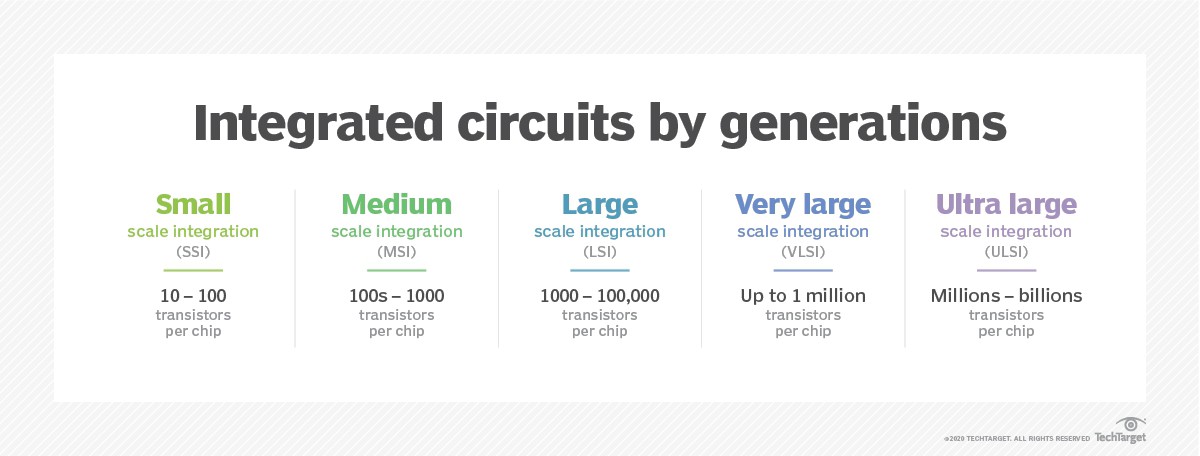
Figure 1. Integrated circuits by generations
In fact, there are many other uses for integrated circuits beyond the common knowledge that they are the central technology of electronics, for example: an Integrated Circuit (IC) can operate as a logic gate, oscillator, counter, timer, amplifier, microprocessor, microcontroller, or computer memory [1].
An Integrated Circuit (IC), also known as a chip or microchip, includes various electronic circuits assembled on a compact, flat piece of semiconductor material, typically silicon.
So, how do ICs work? ICs operate through the integration of various electronic components within a silicon-based semiconductor. This process enables efficient data processing and signal transmission. A intricate network of channels, engraved onto the chip's surface, interlinks these elements. These channels facilitate the movement of electrical signals among the components, allowing the IC to execute particular tasks, such as data processing, signal amplification, or information storage.
The history of the creation of integrated circuits is very strange and fascinating, here is a short introduction to the "three fathers" of integrated circuits. The concept of embedding electronic circuits into a singular device emerged when Geoffrey Dummer, a British radio engineer, suggested consolidating various standard electronic elements into a monolithic semiconductor crystal in 1952. Earlier, in 1949, Werner Jacobi, a German physicist and engineer, had already created and patented the initial known integrated transistor amplifier. From 1953 to 1957, Sidney Darlington and Yasuo Tarui introduced chip designs enabling multiple transistors to coexist within a shared active area, though they lacked electrical isolation to distinguish them from one another.
Three people created integrated circuits without using them, it is peculiar that they were unaware of each other or had no insight into one another's endeavors. As shown in Figure 2, the original integrated circuit was created by Jack Kilby. While Geoffrey Dummer envisioned the design, Robert Noyce secured the initial patent, and Jack Kilby’s submission was under evaluation during the time the first patent was issued [2].
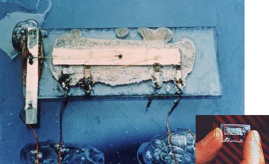
Figure 2. The original integrated circuit created by Jack Kilby [3]
ICs contain small circuits made of transistors. Integrated circuits have three mainly different with chips, they’re “Different effects, Different shapes and packages and Made differently.” There are also two reasons for this in terms of different usage effects: As per Moore's Principle, the amount of transistors inside an integrated circuit increases twofold approximately every 18 months, allowing for greater circuit integration on a single chip. Increasing the capacity within a given area helps lower costs while enhancing efficiency [4]. Chips, which are commonly produced on the surface of semiconductor wafers, are a method for miniaturizing circuits. The use of lithography to pattern an entire circuit onto a chip, which can contain up to billions of individual transistors, makes integrated circuits made from silicon. Other kinds of common components such as resistors, capacitors, and inductors can also be patterned onto the same chip, all at microscopic sizes, permitting enormously complex designs to be created in a very small device [5].
A microchip is a small, densely packed electronic unit. The distinction lies in their shapes and packaging. Integrated circuits, fabricated on one or more thin semiconductor layers or insulating bases. The chip itself is manufactured using a single crystal silicon wafer.
It's not a bad idea to take a look at the transistors, an integral part of the integrated circuit.
Transistors are important in that there are five great advantages, such as Switching, Amplification, Miniaturization, Efficiency, and Rugged. Electronic switches that are excellent are transistors. Transistors can rapidly alternate currents, switching on and off billions of times each second and executing millions of operations within that duration. The majority of audio and signal amplifiers depend on transistor-based technology.
Depending on their use, transistors can be manufactured to be extremely compact and energy-efficient. They are utilized in military, space, and industrial settings due to their ability to endure severe shock and vibration [6]. A transistor that can withstand significant current flows can be constructed using a monolithic piece of doped silicon.
As shown in Figure 3, the rapid advancement of transistors is evident, demonstrating how the transistor count on microchips doubles approximately every two years, providing evidence for Moore's Law.
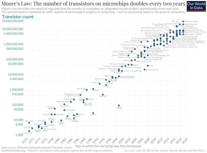
Figure 3. Moore's Law: The number of transistors on microchips doubles every two years [7]
Within a decade of its creation, the transistor transformed modern electronics and research institutions. Physicists worldwide eagerly explored the possibilities of transistor technology.
Although transistor have not been around for a long time, physicists have been coveted by many of his unique properties. Physicists worldwide have been frantically investing money and time in researching transistors. If the development without resistors, internet, mobile phones, and medicine, transportation systems may never have existed.
Semiconductors play a crucial role as essential elements within Integrated Circuits (ICs). Moving forward, let's delve into what a semiconductor is: it refers to a crystalline solid whose electrical conductivity is intermediate between that of conductors and insulators. The manufacturing process of silicon-based semiconductors is also discussed in detail. Silicon Ingots, Slicing and Cleaning, Photolithography, Layering, The final product. Silicon is usually extracted from naturally occurring silica and is generally heated to 1420 degrees and put into a mixture that is pulled out. This creates very fine slices, which subsequently need to be cleaned. Further polishing to get them to a certain thickness. The material is then photolithographed, covered with a layer of photoresist, and placed under ultraviolet light. To build the circuit, a portion of the photoresist is washed away. The remaining photoresist makes up the circuit pattern. The final manufacture of a single semiconductor takes a very long time—up to four months on board—and is a very delicate facility and requires great care in the manufacturing process. An interesting tidbit – The yellow light commonly observed in images of semiconductor fabrication facilities originates from the lithography rooms. Since the photoresist material is reactive to high-frequency light, UV light is employed to render it soluble. To prevent harm to the remaining portions of the wafer, the rooms are illuminated with low-frequency yellow light.
The photolithography process can be iterated multiple times to produce the necessary patterns on each wafer. It is during this phase that the outlines of each individual rectangular chip are also imprinted onto the wafer [8].
In 1956, William Shockley, John Bardeen, and Walter Brattain from Bell Labs received the Nobel Prize in Physics for their groundbreaking research on the field of semiconductors and the uncovering of the transistor effect.
The primary goal of the study is to gain a comprehensive understanding of integrated circuits, to know why silicon has been used as the dominant material to make integrated circuits, why there is a need for alternative materials to replace silicon, and the characteristics of alternative materials, and the comparison of the characteristics of alternative materials and silicon. In reality, substitution can be realized or not because of the hindrances brought about by three influencing factors.
2. Research review
The paper explains that the purpose of silicon in integrated circuits, the development of silicon in ICs. And the demand of integrated circuits. So, the papers in research review that chosen are most closely match the views and were relevant to the area of research. The review is based in twelve areas and created a general detailed of what were all talking about, and then filled in data and douc to finish the literature review.
2.1. What is IC
Based on their design, Integrated circuits can be classified into three primary categories: Analog Integrated Circuits, Mixed Integrated Circuits, and Digital Integrated Circuits. Among these, Digital Integrated Circuits are specifically designed to handle discrete signals and interpret binary data, which consists of values like 0 and 1. Usually composed of logic gates, multiplexers, and potentially an amplifier or a broad microprocessor, they play a crucial role in digital signal processing. Before the emergence of microprocessors and advanced design tools, Analog Integrated Circuits were developed for manual computations. They commonly incorporate operational amplifiers, voltage regulators, active filters, and phase-locked loops, with power gain, power dissipation, and resistance being key factors in their design. Mixed Integrated Circuits, conversely, integrate elements of both analog and digital circuits, enabling them to perform analog - to - digital or digital - to - analog conversions.
Digital integrated circuits find widespread application in various fields, including microprocessors, computing systems, computer networks, frequency counters, and digital signal processors. This category encompasses various subcategories, including programmable integrated circuits, logic controllers, Memory chips, interface integrated circuits, and power management integrated circuits are also key applications of digital ICs. On the other hand, analog integrated circuits are exemplified by designs such as power management circuits, operational amplifiers, and transducers. These components process continuous signals to perform tasks like active filtering and other specialized functions, on-chip power distribution, mixing, and more. Mixed-signal integrated circuits find applications in numerous fields such as mobile phones, Modern communication and sensor technologies frequently incorporate integrated circuits featuring standardized digital interfaces such as I2C, UART, SPI, or CAN. These components are essential in various fields, including voice signal processing, aerospace technology, IoT applications, drone technology, and electric vehicle development. The integration of analog and digital functionalities within a single chip offers economical advantages for manufacturing a wide range of products, from everyday electronic devices to specialized equipment used in healthcare, industrial settings, scientific measurement, and space exploration.
2.2. Semiconductors
Semiconductors are essential in manufacturing a wide range of electronic components, such as diodes, transistors, and integrated circuits. These components are widely adopted because of their significant benefits, such as small size, exceptional reliability, superior energy efficiency, and affordability. The employment of semiconductors as discrete components has been well-recorded in various applications, like electronic devices, sensors, and light-emitting components, with solid-state lasers being a prime example.
With the application of semiconductors, there are many types of semiconductors, as shown in Figure 4.
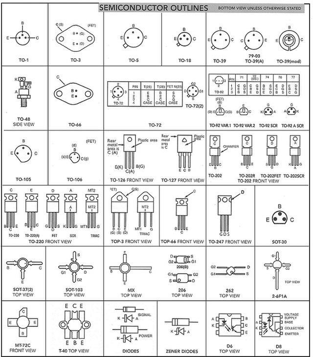
Figure 4. Semiconductor outlines
Before 1947, when the bipolar transistor was developed, semiconductors were mainly two-terminal devices like rectifiers and photodiodes. Semiconductor manufacturing involves six essential steps: deposition, photoresist application, lithography, etching, ionization, and packaging.
Preparing semiconductor materials for integrated circuits requires multiple processes. For example, thermal oxidation creates a layer of silicon oxide on the silicon surface, serving as both a gate insulator and a field oxide. Photomasking and photolithography are also crucial processes. After that, etching is carried out. During the etching stage, the exposed areas of silicon, which were not protected by the photoresist layer in the prior step, are selectively removed. Currently, plasma etching is the most commonly used method for this step. The final step involves the diffusion process, commonly referred to as doping. In this stage, impurity atoms are introduced into the semiconductor system, resulting in the creation of a p-n junction. This junction represents the boundary between p-type and n-type semiconductor materials within a single crystal. The p-type region contains an abundance of holes, while the n-type region has a surplus of neutral electrons in the outer shells of its atoms. This unique property allows current to flow in only one direction across the junction. Due to the minimal amount of semiconductor material used, even slight imperfections can greatly affect its performance [9]. Additionally, achieving a highly flawless crystal structure is critical. Imperfections such as dislocations, twins, and stacking faults can impair the semiconductor's functionality. In fact, crystal defects are the leading cause of failures in semiconductor devices.
2.3. Si development history
In the world, there is a vast array of elements. However, the question remains: why did scientists opt for silicon? There are two primary reasons behind this choice. Firstly, silicon devices demonstrate significantly lower leakage currents. Secondly, Silicon Dioxide (SiO₂), a top-notch insulator, can be easily integrated into silicon-based devices. As a result, silicon technology has advanced remarkably and spread widely. Currently, silicon-based devices account for over 95% of all semiconductor products sold globally [10].
Although silicon is the most commonly used semiconductor material for manufacturing Integrated Circuits (ICs), it is not the only option available.
Solid-state devices are built using semiconductor materials that enable electrical conduction. Semiconductors have an electrical conductivity between 10^-7 and 10^-13 mho/m, positioning them between conductors (conductivity > 10^-7 mho/m) and insulators (conductivity < 10^-13 mho/m). Initially, germanium was used in the production of solid-state devices. However, its high sensitivity to temperature was a major limitation. As manufacturing technologies advanced, silicon gained popularity. This was due to its excellent thermal stability and wide availability [11].
One of the main advantages of silicon is that it is much easier to use in the real world of mass manufacturing. Silicon has a "natural oxide", Silicon Dioxide (SiO2). This readily available insulator is a valuable asset in making silicon devices. Silicon dioxide and carbon react to form silicon and carbon monoxide. Then silicon and chlorine gas react to form silicon chloride. Finally, silicon chloride and magnesium react to form magnesium chloride and silicon. This is how silicon is made from silicon dioxide.
Putting aside theoretical physics for a moment, a material's band gap refers to the space existing between its atomic shells. A wider such space implies that more energy is required to enable the electrons in a semiconductor to "leap" to the subsequent shell layer, thereby transitioning the semiconductor into a conducting state. As will be elaborated later, this concept has numerous significant implications.
In simple terms, relative mobility refers to the average velocity of charge carriers when subjected to an electric field. It is calculated as the ratio of the velocity in meters per second to the electric field strength in volts per meter. The mobility of a semiconductor is influenced by multiple factors, including impurity concentrations, defect levels, temperature, and the concentrations of electrons and holes. Additionally, it is affected by the electric field, especially at high field strengths where velocity saturation takes place. The semiconductor mobility can be measured through the Hall effect or deduced from the behavior of transistors.
The development of silicon in integrated circuits faces several limitations, primarily driven by three key factors. The first issue is the relatively low electron-hole mobility in silicon, which hinders the pursuit of higher performance. To overcome this, manufacturers frequently improve mobility by adding germanium to the silicon [12].
Another issue with silicon is its significant performance decline at elevated temperatures. Contemporary integrated circuits, containing billions of transistors, produce substantial heat, necessitating extensive cooling measures—such as fans and heat sinks commonly seen in desktop computer processors.
Finally, silicon has poor light transmission properties. In modern applications, lasers, LEDs, and similar photonic devices are widely used, but they rely on semiconductor compounds rather than silicon. This has led to the development of two separate industries: one focused on silicon-based electronics and the other on compound-semiconductor-based photonics. However, there is now a significant push towards combining electronics and photonics on a single chip, a trend that holds considerable importance for manufacturers.
2.4. Research on alternative materials
The most commonly employed semiconductor materials are silicon, germanium, and gallium arsenide. While other materials are available, they are typically reserved for specialized components or niche applications.
Take Gallium Arsenide, for example. It is a material formed by combining gallium and arsenic elements. This compound is frequently called a III-V compound since gallium belongs to the III group and arsenic belongs to the V group in the periodic table.
So how to comparisons Material from the three main sources [13].
Gallium arsenide has been in use for a long time. In fact, DARPA (an organization) has been financially supporting research on this technology since the 1970s. Although silicon-based technology has been the fundamental element of the microelectronics revolution, gallium arsenide-based circuits can operate at higher frequencies and have greater signal amplification capabilities. These features have made it possible for the world to be connected through palm-sized mobile phones.
In the 1980s, gallium arsenide played a crucial role in the miniaturization of GPS receivers. Its application enabled the development of laser-guided, precision munitions that were incorporated into the arsenals of the United States during that era.
Gallium arsenide has high electron mobility, which enables semiconductor devices made from it to operate at frequencies reaching into the hundreds of GHz. Although it isn't strictly regarded as a "wide bandgap" material, its bandgap is significantly larger than that of silicon.
Gallium arsenide is regarded as an excellent option due to its transistors operating at speeds five times faster than those of silicon. Despite this, silicon continues to dominate as the most commonly used semiconductor material. Gallium arsenide stands out as a unique alternative with no direct equivalent.
Germanium still finds applications in certain areas. Notably, reintroducing germanium into semiconductor materials isn't as difficult as it might appear. According to reports, certain chips showcased in a 2015 demonstration of advanced chip-manufacturing technology by IBM and its partners incorporate transistors that use a silicon-germanium blend in the channel.
These developments could potentially signify the start of an industry trend towards using a larger proportion of germanium in transistor channels. In the future, transistor materials may bring about a new era of improved performance.
In the late 19th century, German chemist Clemens Winkler first isolated and recognized germanium. Named after Winkler's hometown, it was initially classified as a metal with low conductivity. However, during World War II, its semiconducting properties—such as the ability to alternate between conducting and blocking electrical currents—were discovered, fundamentally altering this perception.
After the war, solid-state devices using germanium saw rapid expansion, with U.S. production skyrocketing from a few hundred pounds in 1946 to 45 tons by 1960. However, silicon ultimately emerged as the preferred material for manufacturing logic and memory chips, surpassing germanium in popularity [14].
Three properties that primarily determine IC material selection are below. The bandgaps, intrinsic carriers and relative mobility.
The data of the three types of materials Bandgaps are shown in Table 1 [15].
Table 1. Comparison of Bandgaps of Silicon, Germanium and Gallium Arllium
Silicon (SI) | 1.1 |
Germanium (GE) | 0.87 |
Gallium Arllium (GAAS) | 1.4 |
As noted earlier, silicon, germanium, and gallium arsenide remain the most widely utilized intrinsic semiconductors in the production of Integrated Circuits (ICs).
The free electrons present in intrinsic materials are referred to as intrinsic carriers. The concentrations of these carriers (measured per cubic centimeter) for the respective materials are in Table 2.
Table 2. Intrinsic carrier concentrations of Silicon, Germanium and Gallium Arllium [16]
Silicon | 1.5*10^10 |
Germanium | 2.5*10^13 |
Gallium Arllium | 1.7*10^6 |
Relative mobility is another critical factor, as it influences how easily free carriers can travel within the material. The relative mobility values of these materials are shown in Table 3.
Table 3. The relative mobility values of Silicon, Germanium and Gallium Arllium
SILICON | 1500cm |
GERMANIUM | 3900cm |
GALLIUM ARSENIDE | 8500cm |
It is worth noting that gallium arsenide has the lowest concentration of intrinsic carriers but the highest relative mobility, which is why devices fabricated with GaAs deliver the fastest response speeds.
In summary, the advantages and disadvantages of germanium over silicon are Germanium is not an abundant material. It is more expensive, heavy and fragile than silicon. It has a lower energy band gap and hence higher junction leakage current. Excessive leakage currents can hasten device deterioration and shorten the functional lifespan of GaN FETs. To overcome these disadvantages, it is likely that germanium will be used in the form of a thin layer on an insulating substrate. In general, Germanium on Insulator (GeOI) refers to a thin layer of germanium on a silicon oxide substrate. Germanium is still used in some applications [17].
Since the 1990s, Gallium Nitride (GaN), a III/V direct-bandgap semiconductor, has been widely used in blue light-emitting diodes. Due to its remarkable current-conduction properties, GaN transistors are well-suited for applications requiring high frequency, high voltage, high temperature, and high efficiency. Although GaN has advantages over silicon, like higher energy efficiency, faster performance, and better recovery properties, it also faces challenges. These include the depletion-mode characteristic of GaN transistors and difficulties in scaling up production to the same volume as silicon transistors.
GaAs wafers exhibit a wide operating temperature range and excellent thermal stability. Their high resistance to radiation damage makes them suitable for applications in space electronics and as optical windows in high-power systems. Additionally, GaAs cells are not affected by heat, meaning they are highly resistant to overheating.
But his disadvantages are: unlike silicon, GaAs does not contain any natural oxides. On top of that, it has the expensive production costs of single-crystal GaAs substrates. Lastly, the size of the ingot is relatively small when compared to silicon [19].
Beyond silicon-based chips, there are multiple alternative options. One alternative is Gallium Nitride (GaN) chips. GaN demonstrates superior electron mobility in comparison to silicon, allowing it to deliver faster switching speeds and improved power efficiency.
As shown in Figure 5, for devices with the same voltage rating, GaN devices excel by offering significantly lower on-resistance per unit area compared to both SiC and Si devices. Consequently, the die and package size of GaN devices are considerably more compact.
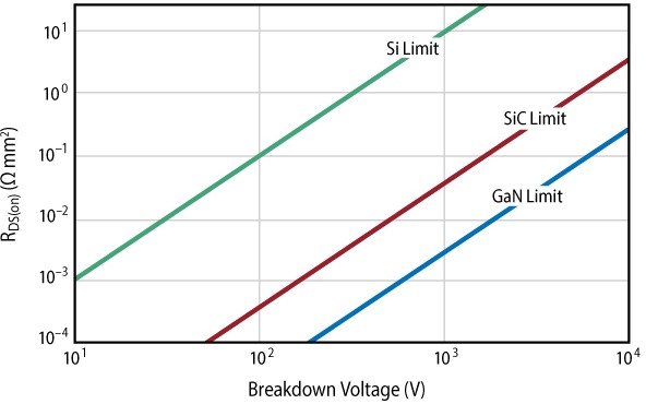
Figure 5. Comparison of material limits in power semiconductors: Si, SiC, and GaN
Since 2014, EPC has been manufacturing GaN ICs with the aim of advancing toward fully integrated systems on a single GaN-on-Si chip, where users provide a logic-level input and receive high-performance power conversion as output. These systems are smaller, faster, more cost-effective, and highly integrated. In summary, this is our response to the question, "Why GaN?" [20].
Gallium Nitride (GaN) is a group III/V direct bandgap semiconductor that has been extensively utilized in blue LED technology since the 1990s. Due to its ability to conduct current efficiently, GaN transistors are well-suited for applications requiring high frequency, voltage, temperature, and efficiency. Despite its advantages over silicon, such as greater energy efficiency, faster performance, and superior recovery properties, challenges remain, including the depletion-mode nature of GaN transistors and limitations in scaling production to match silicon transistor volumes [21].
Organic electronics rely on carbon-based materials and are being investigated for use in flexible and large-area electronic devices. Additionally, other chip alternatives include graphene chips and carbon nanotube chips.
Graphene chips: Known for their exceptional electron mobility, thermal conductivity, and mechanical strength, graphene is being explored for electronic applications. However, it has yet to be commercially adopted.
Carbon Nanotube (CNT) chips: With outstanding thermal conductivity and mechanical durability, CNTs are highly suitable for high-power applications.
Carbon Nanotubes (CNTs), essentially small cylindrical structures made from graphene sheets, possess superior electrical and thermal properties compared to silicon. However, a significant obstacle exists in converting them into high-purity tubes for integration into chips. Although a purity level of 99.99% can be achieved, even a minute degree of impurity raises concerns and may impede or halt the switching operation of transistors. To prevent such failures, advanced circuits would require CNTs with a purity of approximately 99.999999%, which is currently nearly impossible to produce, thus precluding their mass production.
Nonetheless, CNTs are still employed in numerous other applications. With continued research, they remain a potential substitute for silicon chips. In fact, major chip-making companies like TSMC, IBM, and Intel, along with numerous research institutions and universities, are actively researching CNT-based chips. A DARPA-led project is working on 3D devices that integrate memory layers with carbon nanotube transistors.
According to a news release from the Massachusetts Institute of Technology, silicon has certain limitations. Although it enables electrons to move easily within its structure, it is less effective at supporting "holes," the positively charged counterparts of electrons. For certain types of chips, being able to manage both electrons and holes is crucial. Additionally, silicon has poor heat-conducting properties. This is the reason why overheating problems and costly cooling systems are prevalent in computers [22].
These silicon chip alternatives come with unique characteristics and obstacles, yet they offer the possibility of surpassing the performance and affordability of existing silicon-based solutions [23].
3. Discussion & development
It is well known that integrated circuits are ubiquitous in our lives. It is difficult for any electronic device to leave integrated circuits, from the old-fashioned desktop computers that cannot be moved to mobile phones that are used every minute of every day, all of which require integrated circuits.
People all over the world need the help of integrated circuits if they use mobile phones, so the number of integrated circuits produced every year is huge and the market demand is high. A complete related industry chain has been formed, so many people have chosen to work in related jobs, starting from the source, collecting the materials (such as silicon) needed to make integrated circuits, delivering the materials, making the simplest silicon wafers, and also needing managers to help manage the production of the agency. Technicians are also needed to design integrated circuits, experiment with feasibility, and then find companies to distribute them and sell them.
Because of the scarcity of integrated circuits, if there is a very new and accomplished product, then the country that researched it will also have a dominant position in the world, such as a book called Chip Wars. It's talking about the capital wars behind the chips.
So, in terms of manpower, in terms of economics, and in terms of politics, there is a need to use this to explore the feasibility of the materials listed in literature review.
In order to understand the feasibility of silicon being replaced by Ge or GaAs as a material for integrated circuits. First of all, it is necessary to know the impact of silicon on the world in three areas: humanities, economics, and politics. So, since silicon is in high demand to be used to make integrated circuits, there is a need for countries to produce silicon.
3.1. Societal and political impact of silicon
3.1.1. Production
As shown in Table 4, the ranking of countries that will produce silicon in 2023 is presented.
Table 4. Global silicon production by country (1000 tons/year) in 2023 [24]
Country | Silicon Production (1000 tons/year) |
China | 6,000 |
Russia | 580 |
Brazil | 390 |
Norway | 350 |
United States | 310 |
France | 120 |
Iceland | 110 |
Malaysia | 80 |
As the data shows, every year the production of silicon can be more, especially China. There are almost 6,000,000 tons of production silicon in China, so it is clear that China has absolute leadership in silicon production. China's silicon production is almost ten times that of second-place Russia, which shows how big the gap is. In addition to China, other countries in the top ten, the sum of the production of other countries cannot reach China's production.
So, is it a coincidence that production is dominated by China? If not, when did the domination by China begin? A bar chart data below, as early as ten years ago, 2010-2011, China's silicon production has been in the dominant position.
Production and Domestic Usage of Organic Silicon Monomer in China, 2001-2011
As indicated in Figure 6., back in 2011, ten years ago, China was exporting 1,100,000 tons of silicon per year. So back ten years ago, China was already very strong in manufacturing silicon.
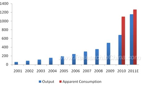
Figure 6. China's annual silicon exports from 2001 to 2011 [25]
In fact, the main reason why China can produce so much silicon in one year is that there are so many people and so much labor. China's silicon manufacturing industry has a large number of skilled labors, which helps improve China's competitiveness in the global market. It will explore the skilled workforce in China’s silicone manufacturing industry, highlighting their contributions to efficiency and productivity, along with case studies showcasing their impact.
China's silicone manufacturing industry is home to a highly proficient workforce, and this brings multiple advantages to companies, particularly in enhancing efficiency and productivity. Chinese manufacturers have the advantage of a vast reservoir of skilled labor at their disposal. This enables them to quickly expand production levels, effectively keeping up with the increasing market demand. Moreover, these skilled workers possess the expertise required to operate state-of-the-art manufacturing equipment. Their capabilities not only contribute to a boost in production efficiency but also help in cutting down production costs [26].
As CS Connected stated, each direct semiconductor job generates nearly six additional jobs in related industrial supply chains and the broader economy [27]. According to China Customs data, in 2022, China shipped out 94 metric tons of gallium, marking a 25% rise from the year before.
The USGS reported that the production of high-purity refined gallium in 2022 was approximately 290,000 kilograms, a 16% increase from 250,000 kilograms in 2021 [26].
Gallium is found in small quantities in zinc ore and bauxite, and is extracted during the aluminum production process from bauxite. The CRMA reports that China produces approximately 80% of the world’s gallium supply. This element is used in the manufacturing of gallium arsenide, an essential material in electronics. According to the Critical Raw Materials Alliance (CRMA), only a limited number of companies—one in Europe, and the others in Japan and China—are capable of producing gallium arsenide with the required purity. Additionally, Neo Performance Materials in Canada also claims to have the ability to produce gallium that meets these purity standards [28].
Where was germanium discovered? Germanium ore is extremely scarce, with the majority of germanium obtained as a byproduct of zinc refining and coal ash processing. The Critical Raw Materials Alliance (CRMA), a European industry group, reports that China accounts for approximately 60% of global germanium production, while the remainder is sourced from Canada, Finland, Russia, and the United States [29].
3.1.2. Health
In fact, when workers manufacture silicon, there is an impact on both labor and the environment. This is because manufacturing silicon can be hazardous to human health and is also very harmful in terms of carbon emissions.
Silicon manufacturing poses multiple risks. Workers are exposed to crystalline silica, a raw material. Inhalation of silica can lead to different types of silicosis, including chronic, accelerated, or acute forms. It is also associated with bronchitis, tuberculosis, and some research links it to lung cancer. Workers may also be exposed to silica dust, and control measures are similar to those for crystalline silica. Furthermore, during production, workers may be exposed to hydrogen chloride gas, which can irritate and corrode the eyes, skin, and mucous membranes. Prolonged or high-level exposure may lead to conditions such as laryngitis, bronchitis, and pulmonary edema [30].
Some people assert that high-dose germanium consumption can strengthen the immune system, increase oxygen supply, boost energy, and counteract harmful free radicals, and it's also thought to protect against radiation. Nevertheless, in 1989, the UK Department of Health issued a warning that germanium supplements offer no nutritional or medical benefits and could present health hazards [31]. Germane and germanium tetrachloride are highly combustible and can explode when exposed to air. Inhalation may cause abdominal cramps, a burning sensation, and coughing. Skin contact can lead to redness and pain, and eye exposure can result in redness and pain.
Some gallium compounds are hazardous to health. For example, short-term exposure to gallium (III) chloride can irritate the throat, cause respiratory problems, and chest pain. Its vapors can even cause severe conditions like pulmonary edema and partial paralysis [32].
3.1.3. Environment
In a 2020 paper, Harvard researcher Udit Gupta and his collaborators noted that the production of chips, rather than the consumption of energy or the usage of hardware, is the primary source of carbon emissions from electronic gadgets [33].
Efforts are underway to develop solutions targeting the highly polluting materials utilized in semiconductor production. The industry relies on various gases during manufacturing, many of which contribute substantially to environmental issues.
The issue is that the procedure of extracting gallium can lead to substantial quantities of radioactive substances polluting the water.
In summary, it's the labor and environmental impact of the yield given by silicon. So, what are the yields and environmental impacts of the alternative materials, gallium and germanium arsenic?
The manufacturing of microchips has had a significant social impact on developing countries, which is the first point. It's bringing in many economic elites. The second is that the mining and manufacturing regulations have caused damage to the environment. Pure silicon is not naturally occurring, so they produce a lot of carbon dioxide which causes land pollution.
Moreover, the manufacturing of chips requires the use of labor which can cause negative health effects when making chips. Therefore, many employees are suffering from health problems. Despite many companies in these sectors often overlooking such health risks, advancements in science and technology have introduced viable alternatives to silicon [34].
Knowing this, it is clear that the current market is still more in favor of silicon manufacturing. Many countries have invested a lot of labor and have produced a lot of silicon, but silicon is still in short supply. Even though the production of gallium and germanium arsenic is underway, it still does not dominate the market. The hazards caused in the production of silicon are very damaging to the human body, and it is not very friendly to the environment. So, the health of workers who produce silicon is a matter of great concern. In the production of gallium, there is a preference for more specific compounds that are more harmful to people. It is also harmful to the ocean and water, and emits waste gas and water. In the production of germanium arsenic, it is also more harmful to the ocean and water, and the harm to workers mainly comes from flammable and explosive compounds.
3.2. Economics
As shown in Table 5, the prices per kilogram for silicon, gallium, and germanium in December 2023 are presented.
Table 5. The prices per kilogram for silicon, gallium, and germanium in December 2023
Material | Price Per Kilo (USD) |
silicon | 2915.31 |
gallium | 755.80 |
germanium | 2839.40 |
Without delving into in-depth market analysis, the worldwide market for semiconductor silicon wafers was valued at around $1,147.0 million in 2022. It is projected to attain a revised value of $145.1 million by 2028, with a compound annual growth rate (CAGR) of 4.0% throughout the assessment period. Taking into account the economic effects of the health crisis, the segment of the worldwide semiconductor silicon wafer market under 1.5 mm, as a percentage of the 2021 global market, is expected to be worth USD 1.0 million by 2028 [30].
The global gallium market is highly significant, with its trade involving substantial economic value. For instance, a 2022 study by U.S. Geological Survey (USGS) experts revealed that a 30% disruption in gallium supply could trigger widespread economic consequences, potentially reducing U.S. economic output by approximately $600 billion, equivalent to 2.1% of GDP [34]. Various kinds of gallium-related products (which can be used to make semiconductors) are highly sought after. In 2021, the global market for Gallium Nitride (GaN) semiconductor devices was valued at USD 1.75 billion. It is expected that by 2030, this market will expand to USD 11.03 billion, with a Compound Annual Growth Rate (CAGR) of 21.70% from 2022 to 2030.The power semiconductors segment is leading the market, and it is projected to grow at a CAGR of 21.60% during the same time frame [35]. The gallium oxide semiconductor market is categorized by technology into molecular beam epitaxy, chemical vapor deposition, chemical synthesis, thermal evaporation, and sublimation. In 2022, the molecular beam epitaxy segment led with revenues of USD 2.9 million [35]. Furthermore, as per the U.S. Geological Survey, in 2022, the United States imported gallium metal and Gallium Arsenide (GaAs) wafers valued at around 3 million and 200 million, respectively.
As shown in Figure 7, the economic forecast for gallium oxide—one of the products of gallium —indicates an upward trend with exponential growth. In 2030, the amount can reach 196.23 Mn.
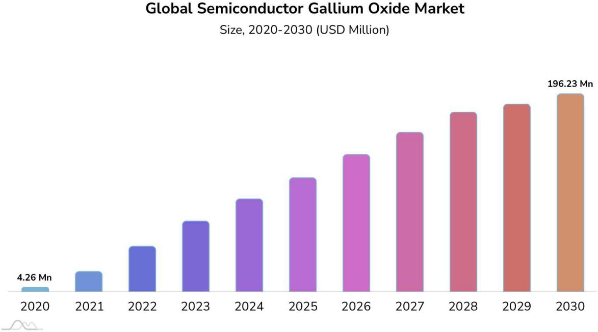
Figure 7. Global semiconductor gallium oxide market (2020–2030) [36]
According to the U.S. Geological Survey (USGS), germanium consumption was about $39 million last year, up 10 percent from 2021.The economic forecast for Germanium products was: The global germanium market shows strong potential, particularly in the solar sector. Despite a downturn in 2020 caused by the COVID-19-induced economic slowdown, the market is projected to rebound in 2021 and grow at a Compound Annual Growth Rate (CAGR) of 7% to 8% between 2020 and 2025 [37]. Key factors driving this growth include increasing demand for fiber optics in communication networks and the trend toward smaller electronic components.
As shown in Figure 8, the projected economic market price of Germanium from 2023 to 2030 is depicted. You can see it's still growing and there's value for money in investing. It's just not growing as aggressively as gallium.
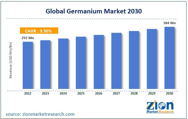
Figure 8. Global Germanium market forecast (2022–2030) [38]
3.3. Politically
However, since China has started to restrict the export of Germanium, the next economic situation is anyone's guess. Even if some countries have started to research and produce Germanium, it is not known whether they can take China's place, whether the production is up to the standard, and whether the products are qualified to be used. The introduction of the policy of restricting exports has led to a significant increase in the price of Germanium now, and has also caused a great deal of price volatility. Since the start of 2023, the price of germanium has risen by 1,650 CNY/Kg, marking a 20.75% increase, based on trading data from a Contract for Difference (CFD) linked to its benchmark market. The metal previously hit a record high of 10,450 CNY in May 2018 [39].
As mentioned earlier, China is going to control the export of materials that can be substituted for silicon, and the international trade market is very sensational about this. In particular, the matter has been analyzed and reported on by developed countries like the United States and the United Kingdom. In the international situation, then, it is also politically unknown whether substitutable materials will be viable.
Why did China introduce these restrictions at this time? Over the past year, the US government has been actively persuading its allies to jointly limit China's access to high-end chip-making equipment, such as lithography machines. This lobbying effort has started to bear fruit. In June, Japan and the Netherlands revealed plans to limit exports of semiconductor-related materials and machinery to China. This has placed significant pressure on China, prompting efforts to engage in discussions with the U.S. regarding these restrictions.
Have been unsuccessful [40]. Because China controls the global supply of critical high-tech metals, making its export restrictions highly impactful. Starting August 1, 2023, these measures will target gallium, germanium, and related compounds. Exporters who wish to start or continue exporting gallium and germanium abroad will need to apply for a license from the Ministry of Commerce. According to China, the new licensing system is designed to safeguard national security [41].
China leads in the production of critical high-tech metals, including gallium and germanium, which are crucial for semiconductors, telecommunications, electric vehicles, and various industries. These metals also play a significant role in defense applications, including radar systems, high-power lasers, and reconnaissance satellites. As China has expanded its production share, other nations like Germany and Kazakhstan have scaled back their output. Additional producers include Japan, South Korea, and Russia for gallium, with global production reaching approximately 10,000 metric tons in 2021, according to the USGS. Germanium is also produced in the U.S., Canada, Belgium, and Russia [42].
China has often criticized the US for practicing "tech hegemony" in reaction to the export restrictions implemented by Washington. Recently, Beijing has also placed restrictions regarding US companies that have connections with the American military, like the aerospace firm Lockheed Martin. At the same time, Western governments have emphasized the necessity of "de-risking" from China, which implies reducing dependence on China for both raw goods and final products [43]. Expanding delivery networks and construction capabilities to extract and refine metals such as gallium and germanium will require significant time. Over the long term, resource-rich nations like Australia and Canada view the resource scarcity as a chance.
Specialists caution that leveraging materials and technical advancements as strategic tools, a tactic employed by both the U.S. and China, could lead to worldwide environmental impacts. This is because essential green technologies depend on these very materials. "This transcends national boundaries—it's a global challenge," noted Dr. Harper. "Ideally, policymakers will collaborate to secure access to these critical resources necessary for the energy transition, enabling progress in tackling decarbonization challenges."
While the latest export controls may not have a catastrophic effect on the the market or buyers, experts emphasize the importance of monitoring the direction in which this trend is evolving.
The U.S. Government has noted that although defense manufacturers represent a minor share of global GaN usage, potential shortages and supply chain disruptions for semiconductors and critical electronics could create long-term issues for defense contractors. Key GaN chip suppliers to the U.S. military often rely heavily on commercial sales to sustain their operations. Any disruptions in the commercial sector could hinder their capacity to fulfill the increasing demand for GaN-based systems in defense. These risks have been recognized by Washington and its allies for an extended period [39].
So, we also want to know, China may implement additional export restrictions in the future. Following its controls on gallium and germanium, further measures could be introduced. According to the government-run newspaper China Daily, Wei Jianguo, a former vice minister of commerce in China, stated, "This is merely the the start of China’s retaliatory actions, and China has a variety of additional measures at its disposal. "Gallium and germanium, while important, do not represent the most serious damage that China could inflict in terms of raw materials.
4. Conclusion
In answering the series of questions as to whether or not there will be materials that will take the place of silicon in integrated circuits, this thesis explores the artificial society. Economic as well as political, various views and theories were found to come to the same conclusion in all three areas that there will be materials that will take the place of silicon in the future.
The properties of silicon enable transistors to function effectively at elevated temperatures and with increased current capacities. This makes them especially well-suited for high-power AC applications, which frequently require performance levels reaching hundreds of kilowatts. Germanium is not an abundant material, it is heavier and more fragile than silicon and accelerates the degradation of the parts, it has a shorter lifetime. But he is easier to mass produce. gallium arsenic for that matter, it can operate at higher hertz frequencies and can reduce noise interference.
Two main factors were identified and considered at the societal level, the first being artificial and the second being environmental. After the introduction of silicon as the main crystalline material, many human and financial resources were invested in the production of silicon transistors in various countries, and despite this impressive production, the demand for silicon transistors still exceeded the supply in the market for integrated circuit chips. However, the production of silicon tubes has also caused hazards to workers and environmental hazards. Substitute materials are also on the rise, except that silicon still dominates the market, and with development, the demand for new materials is growing, and countries are more willing to invest in the production of new materials. Substitute materials can still be harmful to mankind and the environment, but in different directions, and generally less harmful than the production of silicon crystalline tubes.
In terms of economic markets, China is the main market for silicon and alternative materials. It was found that gallium, although it has good properties, is more expensive and requires a larger investment to manufacture than the alternative. The alternative gallium, however, is not only cheaper, but also very suitable for mass production. Even though it is slightly less powerful than germanium, it has the potential to be much more economically viable because it is cheaper and more cost-effective.
Politically, China has always dominated the market for alternative materials as well as silicon, suggesting that it has the lion's share of the say. But after China announced restrictions on the export of alternative materials. Many countries have said that the demand for germanium exceeds the supply, and if this is controlled for a long time, it will not be good, so they have also decided to produce their own germanium, but the purity is not as good as that produced by China. The United States has also said that the alternative material germanium is not only as a very good material for integrated circuits wafer body, but also very helpful for national defense.
The results of this study show that there must be materials to replace silicon in the integrated circuit to make the position of the crystal tube body. There is also Moore's Law as an important factor, and since silicon is no longer able to adapt to Moore's Law, there is no way to continue to develop and manufacture it. However, the human world is always moving forward. If the world could join together and really get into the production of alternative materials, a wafer body made of silicon as the main material for integrated circuits. Then the chips will be better developed and have better performance.
References
[1]. Awati, R. (2021). What is an integrated circuit (IC)? A vital component of modern electronics. WhatIs.com. https://www.techtarget.com/whatis/definition/integrated-circuit-IC
[2]. Heather. (2021). Integrated Circuit (IC) Explained—Everything You Need to Know. History Computer. https://history-computer.com/integrated-circuit/
[3]. Wikipedia Contributors. (2025). Integrated circuit. Wikipedia. Wikimedia Foundation.https://en.wikipedia.org/wiki/Integrated_circuit#/media/File:Kilby_solid_circuit.jpg
[4]. UTMEL. (2022). What is the Difference between an Integrated Circuit and a Chip.Utmel.com. Utmel Electronics.https://www.utmel.com/blog/categories/integrated%20circuit/what-is-the-difference-between-an-integrated-circuit-and-a-chip
[5]. Andrew, S. (2019). What is the difference between transistor and integrated circuits? Quora. https://www.quora.com/What-is-the-difference-between-transistor-and-integrated-circuits
[6]. John, P. (2009). Why Are Transistors So Important? Sciencing. https://sciencing.com/transistors-important-5407975.html
[7]. Wikipedia Contributors. (2020). Moore’s law. Wikipedia. Wikimedia Foundation.https://en.wikipedia.org/wiki/Moore%27s_law#/media/File:Moore
[8]. Cyclops, E. (2025). LinkedIn. Linkedin.com. https://www.linkedin.com/pulse/process-making-silicon-semiconductors-cyclops-electronics-ltd
[9]. Neamen, D. A. (2003). Semiconductor physics and devices: Basic principles (3rd ed.). Internet Archive. https://archive.org/details/semiconductor-physics-and-devices-donald-neamen
[10]. The Editors of Encyclopaedia Britannica. (2025). semiconductor. Encyclopaedia Britannica. https://www.britannica.com/science/semiconductor
[11]. Agnihotri, N. (2021). Why silicon still dominates the IC industry. Engineers Garage. https://www.engineersgarage.com/ic-manufacturing-semiconductors-silicon-germanium-
[12]. Hopkinson, M. (2015). What will power the next electronics revolution? World Economic Forum. https://www.weforum.org/stories/2015/08/what-will-power-the-next-electronics-revolution/
[13]. Wikipedia Contributors. (2019). Gallium. Wikipedia. Wikimedia Foundation. https://en.wikipedia.org/wiki/Gallium
[14]. Ye, P. (2016). Germanium Can Take Transistors Where Silicon Can’t. IEEE Spectrum. https://spectrum.ieee.org/germanium-can-take-transistors-where-silicon-cant
[15]. SNU material data center. (2025). SNUMAT. https://www.snumat.com/search?query=Mn
[16]. CAS-Central Authentication Service. (2025). Berkeley.edu. https://inst.eecs.berkeley.edu//~ee105/fa05/handouts/discussions/Discussion1.pdf
[17]. Olajire, A. A. (2014). Review of ASP EOR (alkaline surfactant polymer enhanced oil recovery) technology in the petroleum industry: Prospects and challenges. Energy, 77, 963–982. https://doi.org/10.1016/j.energy.2014.09.005
[18]. Germanium Bonding. (2020). Queen's University Belfast. https://www.qub.ac.uk/research-centres/QAMEC/ResearchActivities/SiliconOnInsulatorSOI/GermaniumBonding/
[19]. GaAs Wafer | Advantages and Disadvantages of GaAs Wafers. (2019). Wafer World. https://www.waferworld.com/post/gaas-wafer-advantages-and-disadvantages-of-gaas-wafers
[20]. Why GaN: Benefits of Gallium Nitride. (2019). EPC. https://epc-co.com/epc/gallium-nitride/why-gan
[21]. Wikipedia Contributors. (2019). Gallium nitride. Wikipedia. Wikimedia Foundation. https://en.wikipedia.org/wiki/Gallium_nitride
[22]. Kaur, D. (2022). Semiconductor: China may have discovered a better chip material than silicon -- here’s what we know. TechWire Asia. https://techwireasia.com/2022/08/semiconductor-china-have-
[23]. Milton, D. (2023). News. Industry EMEA. https://www.industryemea.com/news/64892-beyond-silicon-
[24]. Silicon Production by Country. (2025). World Population Review. https://worldpopulationreview.com/country-rankings/silicon-production-by-country
[25]. ResearchInChina. (2011). Researchinchina.com. http://www.researchinchina.com
[26]. Silicone Manufacturer - Newtop Silicone Manufacturer. (2022). Newtop Silicone Manufacturer. https://www.newtopsilicone.com/silicone-
[27]. Written submission from CSconnected (SEM0023). (2021). Committees of the Parliament of the United Kingdom. https://committees.parliament.uk/writtenevidence/109166/html/
[28]. Cirino, E. (2019). Silicone Safety: Risks, Exposure Sources, Is Silicone Toxic & More. Healthline. https://www.healthline.com/health/body-modification/is-silicone-toxic
[29]. Belton, P. (2021). The computer chip industry has a dirty climate secret. The Guardian. https://www.theguardian.com/environment/2021/sep/18/semiconductor-silicon-chips-carbon-footprint-climate
[30]. Reuters. (2023). What are Gallium and Germanium and which countries are producers? Reuters. https://www.reuters.com/markets/commodities/where-are-strategic-materials-germanium-gallium-produced-2023-07-04/
[31]. TAMTech Water Treatment Solutions. (2025). Water treatment solutions: Gallium chemical properties. Lenntech.com. https://www.lenntech.com/periodic/elements/ga.htm#ixzz8IfWIcQTXhttps://www.lenntec
[32]. Reuters. (2023). What are Gallium and Germanium and which countries are producers? Reuters. https://www.reuters.com/markets/commodities/where-are-strategic-materials-germanium-gallium-produced-2023-07-04/
[33]. Lenntech. (2020). Germanium (Ge) - Chemical properties, Health and Environmental effects.Lenntech.com. https://www.lenntech.com/periodic/elements/ge.h
[34]. Linkedin (2025). Discover thousands of collaborative articles on 2500+ skills. Linkedin.com. https://www.linkedin.com/pulse/semiconductor-silicon-wafer-market-growth
[35]. Siddhi J. (2023). Semiconductor Gallium Oxide Market Size Report [2023-2030]. Kingsresearch.com. https://www.kingsresearch.com/semiconductor-gallium-oxide-market-57
[36]. Lucintel (2025). Germanium Market Report: Trends, Forecast and Competitive Analysis to 2030. Lucintel.com. https://www.lucintel.com/germanium-market.aspx
[37]. Zion Market Research (2023). Global Germanium Market Size, Share, Value and Forecast 2030. Zion Market Research. https://www.zionmarketresearch.com/report/germanium-market
[38]. Trading Economics (2018). Germanium-Price-Chart-Historical Data-News. Tradingeconomics.com. https://tradingeconomics.com/commodity/germanium
[39]. [39] Yang, Z. (2023). China just fought back in the semiconductor exports war. Here’s what you need to know. MIT Technology Review. https://www.technologyreview.com/2023/07/10/1076025/china-export-control-semiconductor-material/
[40]. [40] Manthey, E. (2023). China strikes back in the tech war, restricting exports of gallium and germanium. ING Think. https://think.ing.com/articles/china-strikes-back-in-the-tech-war-restricting-exports-of-gallium-and-germanium/
[41]. [41] Fastmarkets team, & Cefei, S. (2023). Are China’s export curbs on gallium and germanium a political symbol or a real threat? [Update]. Fastmarkets. https://www.fastmarkets.com/insights/are-chinas-export-curbs-on-gallium-and-germanium-a-political-symbol-or-a-real-threat/
[42]. [42] Liang, A., & Marsh, N. (2023). Gallium and germanium: What China’s new move in microchip war means for world. BBC News. https://www.bbc.com/news/business-66118831
[43]. [43] Powers-Riggs, M. P. F., Brian Hart, & Aidan. (2023). Mineral Monopoly: China’s Control over Gallium Is a National Security Threat. Features.csis.org. https://features.csis.org/hiddenreach/china-critical-mineral-gallium/
Cite this article
Wang,R. (2025). Will other materials replace silicon for use in transistors for integrated circuits?. Advances in Engineering Innovation,16(4),60-74.
Data availability
The datasets used and/or analyzed during the current study will be available from the authors upon reasonable request.
Disclaimer/Publisher's Note
The statements, opinions and data contained in all publications are solely those of the individual author(s) and contributor(s) and not of EWA Publishing and/or the editor(s). EWA Publishing and/or the editor(s) disclaim responsibility for any injury to people or property resulting from any ideas, methods, instructions or products referred to in the content.
About volume
Journal:Advances in Engineering Innovation
© 2024 by the author(s). Licensee EWA Publishing, Oxford, UK. This article is an open access article distributed under the terms and
conditions of the Creative Commons Attribution (CC BY) license. Authors who
publish this series agree to the following terms:
1. Authors retain copyright and grant the series right of first publication with the work simultaneously licensed under a Creative Commons
Attribution License that allows others to share the work with an acknowledgment of the work's authorship and initial publication in this
series.
2. Authors are able to enter into separate, additional contractual arrangements for the non-exclusive distribution of the series's published
version of the work (e.g., post it to an institutional repository or publish it in a book), with an acknowledgment of its initial
publication in this series.
3. Authors are permitted and encouraged to post their work online (e.g., in institutional repositories or on their website) prior to and
during the submission process, as it can lead to productive exchanges, as well as earlier and greater citation of published work (See
Open access policy for details).
References
[1]. Awati, R. (2021). What is an integrated circuit (IC)? A vital component of modern electronics. WhatIs.com. https://www.techtarget.com/whatis/definition/integrated-circuit-IC
[2]. Heather. (2021). Integrated Circuit (IC) Explained—Everything You Need to Know. History Computer. https://history-computer.com/integrated-circuit/
[3]. Wikipedia Contributors. (2025). Integrated circuit. Wikipedia. Wikimedia Foundation.https://en.wikipedia.org/wiki/Integrated_circuit#/media/File:Kilby_solid_circuit.jpg
[4]. UTMEL. (2022). What is the Difference between an Integrated Circuit and a Chip.Utmel.com. Utmel Electronics.https://www.utmel.com/blog/categories/integrated%20circuit/what-is-the-difference-between-an-integrated-circuit-and-a-chip
[5]. Andrew, S. (2019). What is the difference between transistor and integrated circuits? Quora. https://www.quora.com/What-is-the-difference-between-transistor-and-integrated-circuits
[6]. John, P. (2009). Why Are Transistors So Important? Sciencing. https://sciencing.com/transistors-important-5407975.html
[7]. Wikipedia Contributors. (2020). Moore’s law. Wikipedia. Wikimedia Foundation.https://en.wikipedia.org/wiki/Moore%27s_law#/media/File:Moore
[8]. Cyclops, E. (2025). LinkedIn. Linkedin.com. https://www.linkedin.com/pulse/process-making-silicon-semiconductors-cyclops-electronics-ltd
[9]. Neamen, D. A. (2003). Semiconductor physics and devices: Basic principles (3rd ed.). Internet Archive. https://archive.org/details/semiconductor-physics-and-devices-donald-neamen
[10]. The Editors of Encyclopaedia Britannica. (2025). semiconductor. Encyclopaedia Britannica. https://www.britannica.com/science/semiconductor
[11]. Agnihotri, N. (2021). Why silicon still dominates the IC industry. Engineers Garage. https://www.engineersgarage.com/ic-manufacturing-semiconductors-silicon-germanium-
[12]. Hopkinson, M. (2015). What will power the next electronics revolution? World Economic Forum. https://www.weforum.org/stories/2015/08/what-will-power-the-next-electronics-revolution/
[13]. Wikipedia Contributors. (2019). Gallium. Wikipedia. Wikimedia Foundation. https://en.wikipedia.org/wiki/Gallium
[14]. Ye, P. (2016). Germanium Can Take Transistors Where Silicon Can’t. IEEE Spectrum. https://spectrum.ieee.org/germanium-can-take-transistors-where-silicon-cant
[15]. SNU material data center. (2025). SNUMAT. https://www.snumat.com/search?query=Mn
[16]. CAS-Central Authentication Service. (2025). Berkeley.edu. https://inst.eecs.berkeley.edu//~ee105/fa05/handouts/discussions/Discussion1.pdf
[17]. Olajire, A. A. (2014). Review of ASP EOR (alkaline surfactant polymer enhanced oil recovery) technology in the petroleum industry: Prospects and challenges. Energy, 77, 963–982. https://doi.org/10.1016/j.energy.2014.09.005
[18]. Germanium Bonding. (2020). Queen's University Belfast. https://www.qub.ac.uk/research-centres/QAMEC/ResearchActivities/SiliconOnInsulatorSOI/GermaniumBonding/
[19]. GaAs Wafer | Advantages and Disadvantages of GaAs Wafers. (2019). Wafer World. https://www.waferworld.com/post/gaas-wafer-advantages-and-disadvantages-of-gaas-wafers
[20]. Why GaN: Benefits of Gallium Nitride. (2019). EPC. https://epc-co.com/epc/gallium-nitride/why-gan
[21]. Wikipedia Contributors. (2019). Gallium nitride. Wikipedia. Wikimedia Foundation. https://en.wikipedia.org/wiki/Gallium_nitride
[22]. Kaur, D. (2022). Semiconductor: China may have discovered a better chip material than silicon -- here’s what we know. TechWire Asia. https://techwireasia.com/2022/08/semiconductor-china-have-
[23]. Milton, D. (2023). News. Industry EMEA. https://www.industryemea.com/news/64892-beyond-silicon-
[24]. Silicon Production by Country. (2025). World Population Review. https://worldpopulationreview.com/country-rankings/silicon-production-by-country
[25]. ResearchInChina. (2011). Researchinchina.com. http://www.researchinchina.com
[26]. Silicone Manufacturer - Newtop Silicone Manufacturer. (2022). Newtop Silicone Manufacturer. https://www.newtopsilicone.com/silicone-
[27]. Written submission from CSconnected (SEM0023). (2021). Committees of the Parliament of the United Kingdom. https://committees.parliament.uk/writtenevidence/109166/html/
[28]. Cirino, E. (2019). Silicone Safety: Risks, Exposure Sources, Is Silicone Toxic & More. Healthline. https://www.healthline.com/health/body-modification/is-silicone-toxic
[29]. Belton, P. (2021). The computer chip industry has a dirty climate secret. The Guardian. https://www.theguardian.com/environment/2021/sep/18/semiconductor-silicon-chips-carbon-footprint-climate
[30]. Reuters. (2023). What are Gallium and Germanium and which countries are producers? Reuters. https://www.reuters.com/markets/commodities/where-are-strategic-materials-germanium-gallium-produced-2023-07-04/
[31]. TAMTech Water Treatment Solutions. (2025). Water treatment solutions: Gallium chemical properties. Lenntech.com. https://www.lenntech.com/periodic/elements/ga.htm#ixzz8IfWIcQTXhttps://www.lenntec
[32]. Reuters. (2023). What are Gallium and Germanium and which countries are producers? Reuters. https://www.reuters.com/markets/commodities/where-are-strategic-materials-germanium-gallium-produced-2023-07-04/
[33]. Lenntech. (2020). Germanium (Ge) - Chemical properties, Health and Environmental effects.Lenntech.com. https://www.lenntech.com/periodic/elements/ge.h
[34]. Linkedin (2025). Discover thousands of collaborative articles on 2500+ skills. Linkedin.com. https://www.linkedin.com/pulse/semiconductor-silicon-wafer-market-growth
[35]. Siddhi J. (2023). Semiconductor Gallium Oxide Market Size Report [2023-2030]. Kingsresearch.com. https://www.kingsresearch.com/semiconductor-gallium-oxide-market-57
[36]. Lucintel (2025). Germanium Market Report: Trends, Forecast and Competitive Analysis to 2030. Lucintel.com. https://www.lucintel.com/germanium-market.aspx
[37]. Zion Market Research (2023). Global Germanium Market Size, Share, Value and Forecast 2030. Zion Market Research. https://www.zionmarketresearch.com/report/germanium-market
[38]. Trading Economics (2018). Germanium-Price-Chart-Historical Data-News. Tradingeconomics.com. https://tradingeconomics.com/commodity/germanium
[39]. [39] Yang, Z. (2023). China just fought back in the semiconductor exports war. Here’s what you need to know. MIT Technology Review. https://www.technologyreview.com/2023/07/10/1076025/china-export-control-semiconductor-material/
[40]. [40] Manthey, E. (2023). China strikes back in the tech war, restricting exports of gallium and germanium. ING Think. https://think.ing.com/articles/china-strikes-back-in-the-tech-war-restricting-exports-of-gallium-and-germanium/
[41]. [41] Fastmarkets team, & Cefei, S. (2023). Are China’s export curbs on gallium and germanium a political symbol or a real threat? [Update]. Fastmarkets. https://www.fastmarkets.com/insights/are-chinas-export-curbs-on-gallium-and-germanium-a-political-symbol-or-a-real-threat/
[42]. [42] Liang, A., & Marsh, N. (2023). Gallium and germanium: What China’s new move in microchip war means for world. BBC News. https://www.bbc.com/news/business-66118831
[43]. [43] Powers-Riggs, M. P. F., Brian Hart, & Aidan. (2023). Mineral Monopoly: China’s Control over Gallium Is a National Security Threat. Features.csis.org. https://features.csis.org/hiddenreach/china-critical-mineral-gallium/