


1. Introduction
In the 1950s, John von Neumann proposed the basic components of a computer, including input devices, output devices, a controller, an arithmetic unit, and memory. A computer inputs signals into memory through binary program instructions, then the arithmetic unit sequentially reads from and executes instructions in memory, storing the results back into memory. Finally, the results are output from memory to output devices. This theory has been widely applied in the manufacturing of modern computers.
However, the components in the von Neumann architecture work independently, fundamentally limiting performance. The frequent data transfer between memory and the arithmetic unit incurs significant performance costs, leading to the "von Neumann bottleneck" and performance issues in modern computers. The human brain, though structurally extremely complex, operates at very low power. Inspired by this, modern scientists have proposed the concept of brain-like computing. Brain-like computing is based on the structure and working principles of the human brain. By increasing hardware for highly parallel computation, it achieves advanced intelligence at a minimal cost that traditional computers cannot easily reach. To achieve functions similar to the human brain, research directions focus on three aspects: constructing architectures that simulate biological neural networks, simulating the functions of biological neurons, and developing devices that emulate synaptic functions. Devices developed for simulating the basic information processing units of biology are collectively called "neuromorphic devices" and can be categorized into two types: synapse devices and neuron devices. Synaptic plasticity is fundamental for the human brain to achieve multiple advanced intelligence capabilities, so existing neuromorphic devices provide support for complex neural network computing and power reduction, holding significant value for developing more intelligent, low-power, brain-like computing systems. However, due to the shared program and data bus, when the CPU operates much faster than memory read/write speeds, the CPU frequently waits for memory data transfers, limiting overall performance by memory speed [1].
This paper first elucidates the limitations of the von Neumann architecture, noting that its independently operating components result in the "von Neumann bottleneck," whereas brain-like computing can achieve efficient parallel computation by simulating the human brain's structure. Neuromorphic devices, as key hardware, are classified into synapse and neuron devices. Next, it introduces semiconductor nanomaterials, categorizing and explaining the characteristics of quantum dots, nanowires, and others—for instance, quantum dots can emit light of different colors based on size adjustment, and nanowires have constrained lateral dimensions. It also details the effects of quantum confinement and surface phenomena, as well as the principles, advantages, and disadvantages of top-down methods (such as mechanical grinding) and bottom-up methods (such as colloidal chemical approaches). Focusing on mechanism and design, the paper dissects synaptic and neuronal structures, explains how memristors and synaptic transistors mimic biology, and highlights how nanomaterial surface/interface effects govern device behavior; nanoscale oscillators and negative-differential-resistance elements are also surveyed. Turning to applications, it contrasts classical image sensors with biomimetic vision systems and outlines vector-matrix multiplication using nanomaterial crossbar arrays. Finally, the paper identifies challenges at the material and device levels and proposes approaches for combination.
2. Classification and basic properties of semiconductor nanomaterials
2.1. Zero-dimensional and one-dimensional nanomaterials
Quantum dots are representative zero-dimensional nanomaterials and are a type of nanoscale semiconductor. When a certain electric field or light pressure is applied to these nanoscale semiconductor materials, they emit light of a specific frequency. The frequency of the emitted light changes with the size of the semiconductor. Therefore, by adjusting the size of this nanoscale semiconductor, the color of the emitted light can be controlled. Because this nanoscale semiconductor has the characteristic of confining electrons and electron holes, which is similar to atoms or molecules in nature, it is called a quantum dot [2].
One-dimensional nanomaterials, or nanowires, can be defined as one-dimensional structures confined to less than 100 nanometers in the transverse direction. Suspended nanowires refer to nanowires with their ends fixed under vacuum conditions. Depending on the constituent materials, nanowires can be classified into different types, including metal nanowires, semiconductor nanowires, and insulating nanowires. Nanowires are produced in laboratories and, as of 2014, have not been found in nature. Nanowires can be fabricated using suspension methods, deposition methods, or elemental synthesis methods. Typical nanowires have an aspect ratio greater than 1000, so they are usually referred to as one-dimensional materials [3].
Quantum confinement effect: When the spacing between energy levels is larger than thermal energy, magnetic energy, electrostatic energy, magnetostatic energy, photon energy, or the condensation energy of the superconducting state, the quantum effects of nanomaterials appear, resulting in changes in their magnetic, optical, acoustic, thermal, electrical, and superconducting properties. Studies show that as particle size decreases, the energy level spacing increases. Band theory indicates that the electronic energy levels near the Fermi level in metals are generally continuous, which is only true at high temperatures or for macroscopic sizes. For ultra-fine particles containing only a finite number of conduction electrons, the energy levels are discrete at low temperatures. For a macroscopic object containing an infinite number of atoms, the energy level spacing δ→0, meaning that for large particles or macroscopic objects, the energy level spacing is almost zero. However, for nanoparticles, the number of atoms is finite and N is small, which results in a nonzero δ, causing splitting of energy level spacing.
Surface effect refers to the phenomenon where, as the dispersion of a material increases, the specific surface area increases, leading to enhanced activity of surface atoms. When particle size is smaller than 0.1 microns, the surface effect becomes significant; for example, for a 1-nanometer particle, surface atoms account for 99%, resulting in a highly chemically active state. Molecules in the surface layer experience asymmetric forces, producing surface tension and adsorption characteristics, with the change in surface Gibbs free energy directly related to the surface area. For gold nanoparticles, as particle size decreases to 1 nanometer, the proportion of surface atoms increases from 20% to 99%, and the increase in dangling bonds leads to structural instability, requiring stabilizers to maintain their quasi-solid form. This effect, together with adsorption forces and the double-layer structure, helps explain the origin of unfrozen water in permafrost, manifesting as the combined action of clay surface molecules and negative charges.
2.2. Main preparation methods of semiconductor nanomaterials
2.2.1. Top-down approach
The top-down approach begins with macro/micrometer-sized bulk raw materials and gradually refines them to the nanoscale through physical/chemical methods such as splitting, etching, and grinding. Here, the mechanical grinding method is introduced. Mechanical grinding harnesses high-speed grinding balls that successively impact, compress, and shear bulk feedstock, driving a progressive cascade of plastic deformation, fracture, and refinement that reduces the material from millimetre scale down to the nanometre range. Key controlling factors include the diameter of the grinding balls, rotation speed, grinding time, and dispersants. Its advantages are simple equipment, high yield, and very low cost; however, the products may easily introduce metal impurities, the crystal structure may have defects, and the size distribution is broad.
2.2.2. Bottom-up approach
This method relies on the "spontaneous aggregation and orderly growth of microscopic units." The core idea is to control reaction conditions so that atoms/molecules first form "nanoscale nuclei" and then gradually grow into the target structure. It is the mainstream method for preparing high-purity, complex-shaped nanomaterials. The principle of the colloidal chemistry method: in an organic solvent, a semiconductor precursor is mixed with a surfactant. When heated to 120-300°C, the precursor decomposes to produce metal and non-metal ions, first forming "nanocrystals," which then slowly grow under controlled temperature and time, ultimately forming quantum dots with uniform sizes.
3. Working mechanism of neuromorphic devices based on semiconductor nanomaterials
3.1. Synapses and neurons
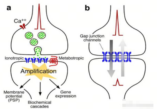
A synapse consists of the presynaptic membrane, the synaptic cleft, and the postsynaptic membrane, which work together to achieve “signal conversion and transmission”. The complete process of synaptic transmission is a conversion of “electrical → chemical → electrical” signals, divided into six steps: the electrical signal reaches the presynaptic membrane; Ca²⁺ channels open, allowing Ca²⁺ influx; synaptic vesicles fuse with the presynaptic membrane, releasing neurotransmitters; neurotransmitters diffuse across the synaptic cleft; neurotransmitters bind to receptors on the postsynaptic membrane (Figure 1). Depending on the receptor type, two effects can occur: excitatory and inhibitory. Neurons transmit information within the cell via “electrical signals”, and their structure is highly adapted to this function, mainly consisting of the soma, dendrites, and axon. The essence of neuronal signaling is changes in the membrane potential, which rely on ion channels on the cell membrane to occur.
3.2. Simulation of prominent devices based on nanodevices
3.2.1. Resistive memory
Resistive memory, also known as resistive RAM, is a new type of storage technology that lies between traditional random-access memory and flash memory. It can combine the advantages of RAM and flash memory to achieve higher storage density and faster data access speeds. Resistive memory is a type of non-volatile memory that uses a novel material called “phase-change material” to function. Programming involves applying an appropriate voltage to change the resistance value of the resistive material, forming or eliminating conductive channels within the material, and storing it as a specific state. As a new type of non-volatile memory, resistive memory has the advantages of simple structure, fast read and write speed, high storage density, and low power consumption, making it a strong candidate for next-generation storage technology. A resistive memory cell has a simple structure, consisting of a top electrode, a dielectric layer, and a bottom electrode. The device exhibits reversible and repeatable resistance switching behavior between a high-resistance state (HRS) and a low-resistance state (LRS) by applying an appropriate external voltage [4].
A synaptic transistor is a new electronic device that mimics the “synapse” function in biological neural systems. Its core characteristic is the ability to modulate “connection strength” via electrical signals like a biological synapse, thereby achieving information storage, processing, and learning [5].
3.2.2. The role of material properties in the design of neural devices
First, nanomaterials have a huge specific surface area, which means that more surface atoms exist per unit volume of material. For example, in synaptic transistors based on indium zinc tin oxide nanowires, the high specific surface area of the nanowires provides abundant adsorption sites for ions. Under an applied electric field, additional ions adsorb onto the nanowire surface, accelerating ionic migration and enabling precise tuning of the device’s conductance—effectively emulating the behavior of biological synapses.
Surface charge distribution affects ion migration direction: The uneven distribution of charges on the surface of nanomaterials creates local electric fields, which influence the direction and speed of ion migration. For instance, in nanophotocapacitor electrodes, the outer TiO₂ shell accepts electrons and then reversibly adsorbs external cations via a non-Faradaic capacitive process, forming a Helmholtz layer. This ion redistribution at the neuron interface depolarizes the cell and initiates action potentials.
Interface effects can promote ion migration. Since various defects such as lattice defects and dislocations often exist at the interfaces of nanomaterials, these defects can serve as channels for ion migration, reducing the energy barrier for ion movement. For example, introducing tin into the crystal structure of binary cation indium zinc oxide forms a homojunction that generates numerous interface defects, facilitating Li⁺ doping and migration in nanowires. Heterojunctions enhance carrier migration and ion trapping: Nanometer-scale heterojunctions composed of different materials can generate unique electronic interactions at the interface due to differing electronic structures and physical properties of each material. For instance, in the J-ZnTPyP@TiO2 core-shell heterostructure, J-aggregated ZnTPyP nanorods act as electron donors, and TiO2 acts as an electron acceptor. After electrons are injected into the conduction band of TiO2, the process drives cations to adsorb on its surface. In addition, in HOFs@Au memristors, the local surface plasmon resonance effect between HOFs and transition metal nanoparticles, along with enhanced carrier transfer, aids in ion trapping and migration, thereby achieving conductivity modulation and simulating synaptic behavior [6].
To achieve the behaviors mentioned above, nanoscopic oscillators are required as supports. Nanoscopic oscillators refer to oscillators with characteristic scales at the nanometer level, mainly including spin nanoscopic oscillators and nano-electromechanical oscillators. Among them, spin nanoscopic oscillators are a novel type of nanoscale microwave device based on magnetoresistance and spin-transfer torque effects. The core structure of nano-electromechanical oscillators is the nano-electromechanical resonator, generally consisting of a driving structure, a nanoscale mechanical resonant structure, and a sensing structure [7]. Furthermore, negative differential resistance devices are a class of electronic devices with special electrical characteristics. Their core feature is the presence of a negative slope region in the current-voltage characteristic curve, meaning that as the applied voltage increases, the current through the device decreases. This abnormal phenomenon, known as the negative differential resistance effect, makes these devices irreplaceable in applications such as high-frequency oscillation, logic circuits, memory units, and signal amplification [8].
4. Research on the application of neural devices
4.1. Brain-like visual perception system
Traditional image sensors have inherent limitations. Specifically, the dynamic range of conventional CMOS sensors typically ranges from 60-80 dB, whereas the human eye can achieve a dynamic range of 120-140 dB. The main issues are overexposure in bright scenes and noise proliferation in low-light scenes. Even with HDR algorithm optimization, multiple frames are required, which increases latency and computational load, making it unsuitable for real-time applications. The “full-pixel readout” mechanism of traditional sensors dictates that increasing spatial resolution requires more pixels. More pixels, however, result in longer signal transmission and processing times per frame, leading to a decrease in frame rate. Conversely, achieving high frame rates requires sacrificing resolution, making it impossible to simultaneously optimize spatial resolution and frame rate.
This is where bionic vision can help. Bionic vision can offer ultra-wide dynamic range and adapt to complex lighting conditions. Additionally, by mimicking the human eye's “pupil adjustment and layered retinal photoreception” mechanism, bionic vision can achieve breakthroughs in dynamic range. At the hardware level, bionic vision uses a “non-uniform pixel array”, with high pixel density in the central field of view and lower density at the edges, while integrating “micro-lenses and variable apertures” to adjust the amount of incoming light in real time. At the signal processing level, bionic vision employs “local contrast enhancement” to automatically suppress signals in bright areas and amplify signals in dark areas, achieving a dynamic range of 120-160 dB, close to that of the human eye [9].
4.2. Implementing core operations using nanomaterial crossbar arrays
Since circuits can transmit signals, they can be used to simulate the computation process in matrix multiplication. The specific steps are as follows: Integrate FGFETs into a matrix and carefully select the corresponding rows and columns to target individual storage elements, forming a crossbar array. The memory in this array uses charge-based storage for computational purposes; both the resistance values and various circuit characteristics are adjustable. By altering the charge quantity in the floating gate (Pt layer), the neutral threshold voltage is shifted, defining different storage states that can be programmed as discrete weights in the matrix for vector-matrix multiplication, thereby enabling vector-matrix multiplication operations [10].
5. Challenges and prospects
5.1. Material level
The high surface energy of nanomaterials makes them prone to adsorbing biomolecules, forming a "bio-corona". This adsorption can alter the surface properties of the material, trigger activation of immune cells, and induce chronic inflammatory responses, manifested as the formation of fibrotic capsules around the device, which isolates the device from neural signal transmission. At the same time, long-term inflammation can damage neurons, leading to neural functional degradation [11].
In addition, the high surface energy of nanomaterials makes them highly prone to aggregation, especially in solution-prepared in vivo environments. After aggregation, the specific surface area of nanomaterials is significantly reduced, and the advantages originally dependent on high specific surface area are completely lost; the micron-sized particles formed by aggregation may block capillaries or be engulfed by immune cells, causing secondary risks such as local thrombosis and inflammation. Aggregation also leads to uneven distribution of materials on device surfaces; for example, nanocoatings on neural electrodes may have “voids” or “thick patches”, causing “blind spots” in signal acquisition or 'noise amplification.'
5.2. Device level
Active semiconductor nanomaterials have a high density of defects at the electrode interface, with an interface state density greater than 10¹² cm⁻²eV⁻¹, which can result in excessive leakage current. This excessive leakage current may cause synaptic weight drift, with a drift amplitude greater than 5% every 10³ cycles. The root of this problem lies in the fact that atomic-level interface control technology is still imperfect. With current processing capabilities, it is difficult to manufacture a perfect interface, thereby affecting the device's ability to accurately process and transmit neural signals, ultimately leading to a neural network classification accuracy reduction of over 15%.
5.3. Core application scenario: implantable neural interface devices
Implantable neural interfaces need to address two core issues: precise acquisition of neural electrical signals and low-damage regulation of neural activity. Narrow bandgap semiconductors, with their low excitation energy and biocompatibility, are ideal candidates. Their primary applications include neural signal sensors and neural modulation electrodes. Neural signal sensors typically detect neural electrical signals in the microvolt range, and traditional metal electrodes are easily affected by noise. In contrast, narrow bandgap semiconductors, with their high carrier mobility and low noise characteristics, can significantly enhance signal acquisition accuracy. Narrow bandgap semiconductor field-effect transistor (FET) sensors, such as those based on black phosphorus or molybdenum telluride, have channel response sensitivity to weak electric fields up to 10⁻⁶ S/V, can be attached to the surface of neural fibers to precisely capture action potentials from individual neurons, and device sizes can be reduced to 100 nm.
5.4. Achieving interdisciplinary communication through the establishment of research teams
Experts in nanomaterials, neuroscience, algorithms, and computer architecture each possess different knowledge systems and research methods. By forming interdisciplinary teams, complementary advantages can be realized. For example, nanomaterial experts can collaborate with neuroscientists to develop suitable nanomaterial devices based on neuroscience needs, such as high-sensitivity nanosensors for neural signal acquisition. Meanwhile, algorithm and computer architecture experts can participate, jointly designing algorithms and systems capable of efficiently processing neuroscience data, achieving comprehensive innovation from materials to system.
6. Conclusion
This paper centers on deploying semiconductor nanomaterials in neuromorphic systems to break the energy-hungry, weakly parallel shackles of traditional von-Neumann computing. It first diagnoses the “storage-computation split” bottleneck, identifies brain-inspired computing as the remedy, and positions neuromorphic devices—split into synaptic and neuronal types—as the critical hardware for emulating biological neural networks. Next, it introduces semiconductor nanomaterials, categorizing and explaining the properties of quantum dots, nanowires, and others—for example, the quantum confinement effect of quantum dots can change optical frequencies, and nanowires have extremely small lateral dimensions. It also analyzes the mechanisms of quantum confinement and surface effects, as well as the principles, advantages, and disadvantages of top-down and bottom-up fabrication methods.
Regarding working mechanisms and applications, the paper analyzes the structure and function of synapses and neurons, explains how devices such as memristors and synaptic transistors mimic biological synapses, and emphasizes the role of surface effects, interface effects, and other factors of nanomaterials in neuromorphic device design. It also introduces nanoscopic oscillators and negative differential resistance devices. In terms of applications, it compares traditional image sensors and explains the advantages of biomimetic visual perception systems, as well as the steps for performing vector-matrix multiplication using nanomaterial crossbar arrays. Finally, the paper points out current challenges at the material level (uncontrolled surface bioactivity, aggregation) and device level (insufficient interface adhesion, high charge transport interface impedance), and proposes the idea of forming interdisciplinary teams in fields such as nanomaterials and neuroscience. It concludes that through structural design and functional regulation, semiconductor nanomaterials can provide a technological pathway for next-generation low-power, highly integrated brain-inspired computing systems, which is of great innovative significance for fields such as artificial intelligence.
References
[1]. Kwon D., Park C. E., Shin W., et al. (2025) Analog Synaptic Devices Based on IGZO Thin‐Film Transistors with a Metal–Ferroelectric–Metal–Insulator–Semiconductor Structure for High‐Performance Neuromorphic Systems [J].Advanced Intelligent Systems,5(12): e2500012.
[2]. Huiwu Shao, Shuo Gao, Ruoyu Wang, et al. (2025) Research Progress on the Preparation, Modification, and Optical Property Regulation of Carbon Quantum Dots Based on Plasma Electrochemical Methods [J/OL].Acta Physica Sinica, pp.1-23.
[3]. Zhongmou Jia. (2022) Quantum Transport Research Based on One-Dimensional Nanowire Superconducting Composite Devices [D]. University of Chinese Academy of Sciences (Institute of Physics, Chinese Academy of Sciences).
[4]. Fu C., Yang J., Wang J., et al. (2024) Dual-Mode Semiconductor Device Enabling Optoelectronic Detection and Neuromorphic Processing with Extended Spectral Responsivity. [J].Advanced materials (Deerfield Beach, Fla.),36(49): e2409406.
[5]. Haorong Qi, Bei Zhang. (2025) Application of Organic Electrochemical Transistors Based on Hybrid Ionic Electrolytes in Neural Synapse Simulation [J].Journal of Functional Materials and Devices, 31(04): 283-291.
[6]. Heng Liu, Miao Ji, Yufei Liu, et al. (2025) Research Progress on Brain-like Learning Characteristics of One-dimensional Memristive Synaptic Devices [J].Electronic Technology,54(01): 7-9.
[7]. Sun Chi. (2024) Hydrogen Response Characteristics of Spin Heterojunctions and Simulation Study of Nanoscopic Oscillators [D]. University of Electronic Science and Technology of China.
[8]. Mao F.L., Li S., Cheng P., et al. (2024) Addressing challenges inverse problem with convolutional neural networks and regulation techniques: Applications in extraction of physical parameters of semiconductors devices [J].International Journal of Electrical Power and Energy Systems,161110172-110172.
[9]. Bingyan Yi. (2025) Research and Application of Visual Bionic Model Based on Deep Spiking Neural Networks [D]. University of Electronic Science and Technology of China.
[10]. Wu Y., Dai S., Liu X., et al. (2024) Optical Microlithography of Perovskite Quantum Dots/Organic Semiconductor Heterojunctions for Neuromorphic Photosensors [J].Advanced Functional Materials, 34(23): 2402136
[11]. Xiaoyan Xu. (2020). Characteristics of the Biological Corona of Nanoparticles and Its Effect on Heavy Metal Adsorption by Nanoparticles [D]. Xiangtan University.
Cite this article
Zhang,S. (2025). Neuromorphic devices based on semiconductor nanomaterials: mechanisms, applications and challenges. Advances in Engineering Innovation,16(10),59-64.
Data availability
The datasets used and/or analyzed during the current study will be available from the authors upon reasonable request.
Disclaimer/Publisher's Note
The statements, opinions and data contained in all publications are solely those of the individual author(s) and contributor(s) and not of EWA Publishing and/or the editor(s). EWA Publishing and/or the editor(s) disclaim responsibility for any injury to people or property resulting from any ideas, methods, instructions or products referred to in the content.
About volume
Journal:Advances in Engineering Innovation
© 2024 by the author(s). Licensee EWA Publishing, Oxford, UK. This article is an open access article distributed under the terms and
conditions of the Creative Commons Attribution (CC BY) license. Authors who
publish this series agree to the following terms:
1. Authors retain copyright and grant the series right of first publication with the work simultaneously licensed under a Creative Commons
Attribution License that allows others to share the work with an acknowledgment of the work's authorship and initial publication in this
series.
2. Authors are able to enter into separate, additional contractual arrangements for the non-exclusive distribution of the series's published
version of the work (e.g., post it to an institutional repository or publish it in a book), with an acknowledgment of its initial
publication in this series.
3. Authors are permitted and encouraged to post their work online (e.g., in institutional repositories or on their website) prior to and
during the submission process, as it can lead to productive exchanges, as well as earlier and greater citation of published work (See
Open access policy for details).
References
[1]. Kwon D., Park C. E., Shin W., et al. (2025) Analog Synaptic Devices Based on IGZO Thin‐Film Transistors with a Metal–Ferroelectric–Metal–Insulator–Semiconductor Structure for High‐Performance Neuromorphic Systems [J].Advanced Intelligent Systems,5(12): e2500012.
[2]. Huiwu Shao, Shuo Gao, Ruoyu Wang, et al. (2025) Research Progress on the Preparation, Modification, and Optical Property Regulation of Carbon Quantum Dots Based on Plasma Electrochemical Methods [J/OL].Acta Physica Sinica, pp.1-23.
[3]. Zhongmou Jia. (2022) Quantum Transport Research Based on One-Dimensional Nanowire Superconducting Composite Devices [D]. University of Chinese Academy of Sciences (Institute of Physics, Chinese Academy of Sciences).
[4]. Fu C., Yang J., Wang J., et al. (2024) Dual-Mode Semiconductor Device Enabling Optoelectronic Detection and Neuromorphic Processing with Extended Spectral Responsivity. [J].Advanced materials (Deerfield Beach, Fla.),36(49): e2409406.
[5]. Haorong Qi, Bei Zhang. (2025) Application of Organic Electrochemical Transistors Based on Hybrid Ionic Electrolytes in Neural Synapse Simulation [J].Journal of Functional Materials and Devices, 31(04): 283-291.
[6]. Heng Liu, Miao Ji, Yufei Liu, et al. (2025) Research Progress on Brain-like Learning Characteristics of One-dimensional Memristive Synaptic Devices [J].Electronic Technology,54(01): 7-9.
[7]. Sun Chi. (2024) Hydrogen Response Characteristics of Spin Heterojunctions and Simulation Study of Nanoscopic Oscillators [D]. University of Electronic Science and Technology of China.
[8]. Mao F.L., Li S., Cheng P., et al. (2024) Addressing challenges inverse problem with convolutional neural networks and regulation techniques: Applications in extraction of physical parameters of semiconductors devices [J].International Journal of Electrical Power and Energy Systems,161110172-110172.
[9]. Bingyan Yi. (2025) Research and Application of Visual Bionic Model Based on Deep Spiking Neural Networks [D]. University of Electronic Science and Technology of China.
[10]. Wu Y., Dai S., Liu X., et al. (2024) Optical Microlithography of Perovskite Quantum Dots/Organic Semiconductor Heterojunctions for Neuromorphic Photosensors [J].Advanced Functional Materials, 34(23): 2402136
[11]. Xiaoyan Xu. (2020). Characteristics of the Biological Corona of Nanoparticles and Its Effect on Heavy Metal Adsorption by Nanoparticles [D]. Xiangtan University.