


1. Introduction
Dr. Peter from the United States first proposed the concept of space solar power stations in the 1960s, where solar energy is directly converted into DC electrical energy in space, then transformed into microwave energy, and transmitted to the ground through a directional antenna [1,2]. In the energy conversion process of space solar power stations, high-voltage and high-power switches, on the order of kilovolts or even tens of kilovolts, are required. Silicon-based power devices can only achieve a voltage level of hundreds of volts. Wide bandgap silicon carbide (SiC) power devices and ultra-wide bandgap gallium oxide (Ga2O3) power devices meet the high-voltage and high-power demands of space solar power stations. However, ultra-wide bandgap gallium oxide power devices are not yet mass-produced and remain at the laboratory development stage, while wide bandgap silicon carbide power devices have already been commercialized and show great potential in meeting the high-voltage and high-power requirements of space solar power stations.
Compared to ordinary ground environments, space solar power stations operate in environments with abundant radiation particles, such as electrons, protons, and heavy ions [3,4]. These radiation particles can cause total dose, single particle, and displacement damage effects on components in space solar power stations [5-10], leading to radiation-induced damage to electronic systems and abnormal operation of space solar power stations [11]. Compared to silicon power devices, wide bandgap power devices have a higher breakdown electric field, meaning that after being hit by radiation particles, the gate oxide of wide bandgap SiC power devices suffers more severe damage than that of silicon power devices. The SiO2 gate oxide in wide bandgap SiC MOSFET power devices is grown on SiC material. Through a relevant process, Si and C are separated, and then Si reacts with oxygen to form SiO2. In contrast, Si MOSFET power devices directly grow SiO2 gate oxide on Si material, where Si reacts with oxygen. Compared to Si MOSFET power devices, the growth process of the SiO2 gate oxide in SiC MOSFET power devices is more complex. Due to the complexity of the growth process and the immaturity of the technology, the reliability of SiC MOSFET power devices is weaker than that of Si MOSFET power devices.
This paper is divided into two parts: The first part reviews the existing research results, studying the issues of wide bandgap SiC MOSFET power devices in space solar power station applications in terms of reliability, total dose effects, and single particle effects. The second part, from an engineering perspective, proposes reinforcement methods based on the failure mechanisms of SiC MOSFET power devices.
2. Issues in the application of wide bandgap power devices in space solar power stations
2.1. Reliability issues
Compared to Si power devices, SiC power devices exhibit notable reliability issues even under conventional environmental conditions, such as threshold voltage drift, short circuits, and surge events. As shown in Fig. 1, the main causes of these reliability issues are material damage, stress, hot carriers, and high temperature. Compared to the failure rate of Si devices, the failure rate of SiC power devices does not follow the typical “bathtub” curve, as illustrated in Fig. 2. Short-term screening (aging) tests cannot effectively eliminate early device failures to improve reliability. The overall failure rate of these devices is relatively high, significantly shortening their service life and adversely affecting long-term reliability [12].
Research by L.H. Wang and others found that repeated switching causes degradation in the threshold voltage and on-resistance of SiC MOSFET power devices [13]. Gonzalez J O and colleagues studied the short-circuit and avalanche characteristics of Si MOSFET and SiC MOSFET power devices. Through experimental comparisons, they found that Si MOSFET power devices have superior short-circuit withstand time and avalanche endurance compared to SiC MOSFET power devices, as shown in Figs. 3 and 4 [14].
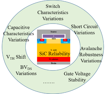
Figure 1. The reliability problems of SiC power devices
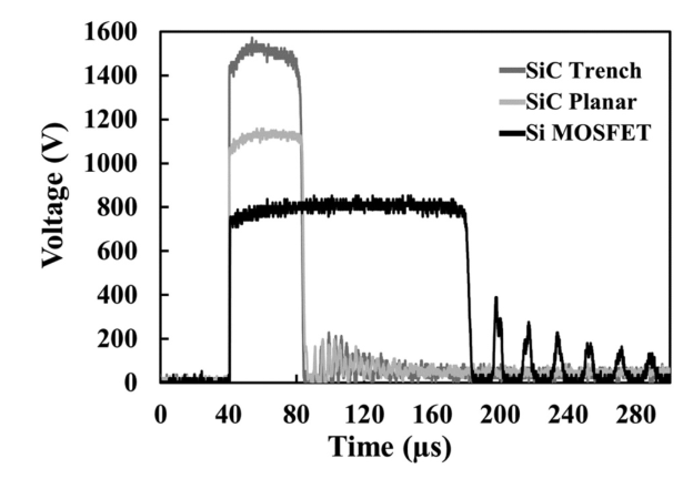
Figure 2. The relationship curves between avalanche times and voltages of Si and SiC devices
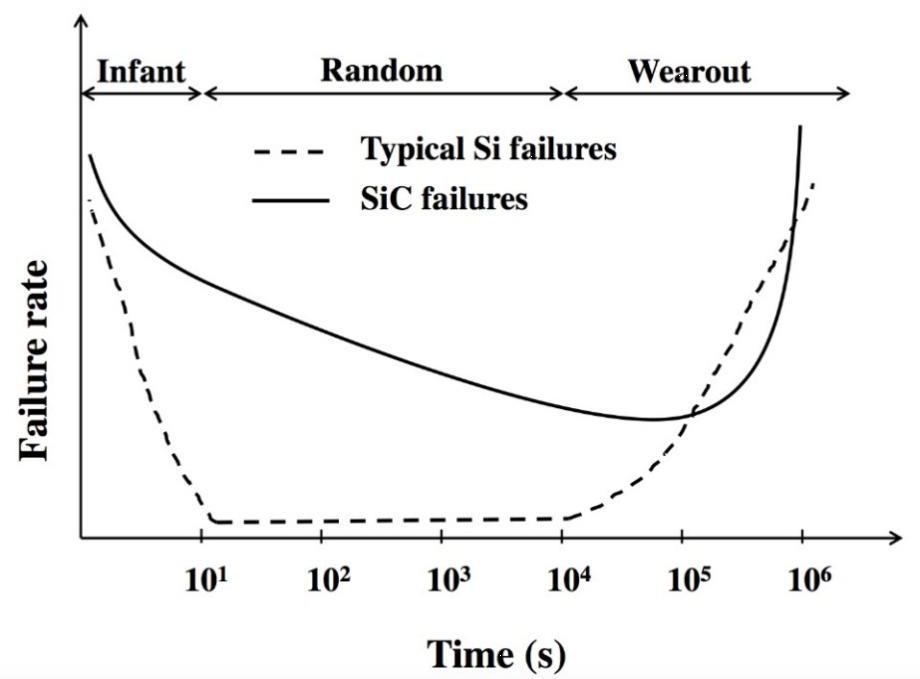
Figure 3. Failure rate curve of Si and SiC devices
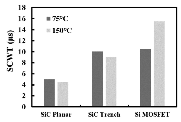
Figure 4. The short-circuit withstand time of Si and SiC devices
2.2. Total dose effect
Popelka and Yu [15,16] studied the total dose effects on commercial SiC MOSFET power devices and found that radiation exposure caused a negative shift in the transfer characteristics of the devices, as shown in Fig. 5. When the radiation dose accumulated reaches 100 krad(Si), the threshold voltage of the device only degrades by approximately 0.25 V. Fig. 6 shows the relationship between the threshold voltage degradation and total dose under different bias conditions for SiC MOSFET power devices. At TID = 100 krad(Si), the threshold voltage degradation is largest under the “on” bias condition, with a degradation of approximately 0.3 V.
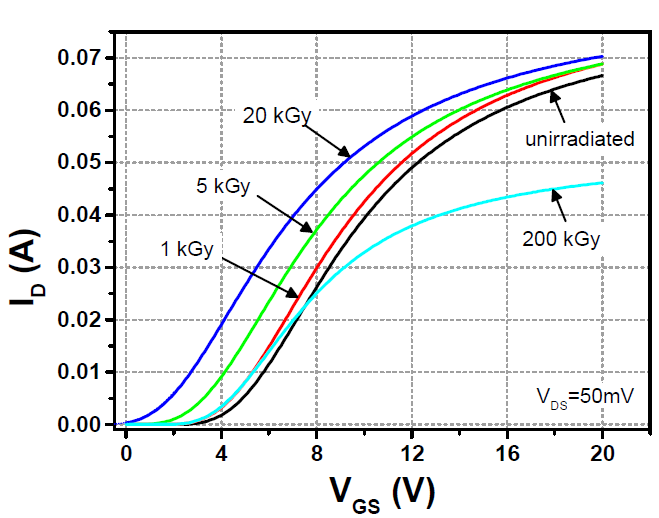
Figure 5. Transfer characteristics degradation of SiC MOSFET power device after TID
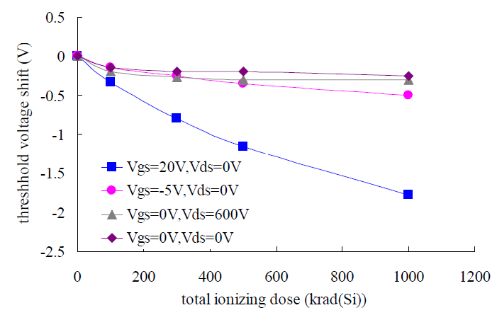
Figure 6. Relationship between threshold voltage of SiC MOSFET power device under different bias and TID
Fig. 7 illustrates the relationship between short-circuit withstand time and short-circuit withstand energy of SiC MOSFET power devices as a function of total dose. It can be seen that as the total dose increases from 0 to 600 krad(Si), the short-circuit withstand capability significantly decreases. Specifically, the short-circuit withstand time decreases from 5.6 µs to 4.6 µs, and the short-circuit withstand energy decreases from 471 mJ to 406 mJ, a reduction of 13.8%. Fig. 8 shows the relationship between avalanche endurance and total dose for SiC MOSFET power devices. As the total dose accumulates from 0 to 600 krad(Si), the avalanche energy decreases from 679 mJ to 507 mJ, a reduction of 25.2%.
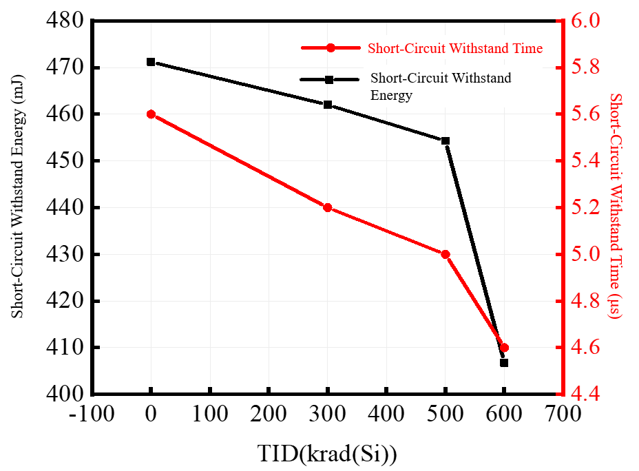
Figure 7. Calculated SCWE and SCWT of planar SiC MOSFET before and after irradiation
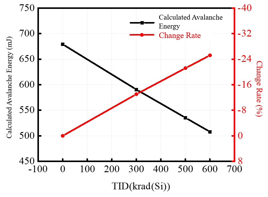
Figure 8. Calculated avalanche energy and change rate of SiC MOSFET power devices before and after irradiation
The total dose induces oxide traps and interface state charges on the gate oxide of SiC MOSFET power devices. These trapped charges lead to a negative shift in the transfer characteristics of the device, with oxide trap charges being the primary factor causing this shift. Radiation-induced trap charges can affect the robustness of the device, thereby impacting its short-circuit withstand capability and avalanche endurance.
2.3. Single event effects
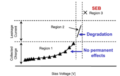
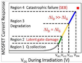
Lauenstein, Martinella, and others [17, 18] studied the single event effects (SEE) in SiC diodes and SiC MOSFET power devices. In SiC diodes, the main single event effect is single event burnout (SEB), while for SiC MOSFET power devices, both single event burnout and single event gate rupture (SEGR) are observed. Under lower drain-source bias conditions, when the SiC diode is subjected to heavy ion irradiation, charge collection occurs inside the device without permanent damage. As the drain-source bias voltage increases, the diode’s leakage current gradually rises, eventually leading to single event burnout, as shown in Figure 9(a). In the case of SiC MOSFET power devices, under low drain-source bias voltage, charge collection occurs without permanent damage following heavy ion bombardment. As the drain-source voltage increases, potential damage appears at the gate oxide, and when the drain-source bias voltage reaches a certain value, leakage currents appear at both the drain and the gate, leading to degradation of electrical characteristics and ultimately single event burnout, as shown in Figure 9(b). A comparison of the single event burnout processes in SiC diodes and SiC MOSFETs, in relation to drain-source bias voltage, shows that the processes are similar.
|
|
(a) SiC diode single event effect results | (b) SiC MOSFET single event effect results |
Figure 9. Relationship between leakage current and drain-source bias voltage for SiC diode and SiC MOSFET power devices after heavy ion irradiation | |
Waskiewicz, Lauenstein, and Ball [19-21] further found that SiC MOSFET power devices and SiC diodes, with the same rated voltage, exhibit very similar threshold voltages for single event burnout after exposure to heavy ion irradiation with the same energy. Figure 10 shows the relationship between the threshold voltage for single event burnout and LET value for SiC diodes and SiC MOSFET power devices. The data indicate that under different LET particle irradiations, the threshold voltage for single event burnout in SiC diodes is close to that of SiC MOSFET power devices.
Since SiC diodes lack parasitic bipolar transistor structures, it was confirmed that the mechanism for single event burnout in SiC MOSFET power devices is different from that in Si MOSFET power devices, where parasitic bipolar conduction causes the burnout [22]. Based on the experimental results in Figures 9 and 10, it was further confirmed that the single event burnout effect in SiC MOSFET power devices is not caused by radiation-induced parasitic bipolar conduction, but rather is similar to that in SiC diodes, being triggered by avalanche effects caused by carrier collision ionization under a local high electric field near the drain junction.
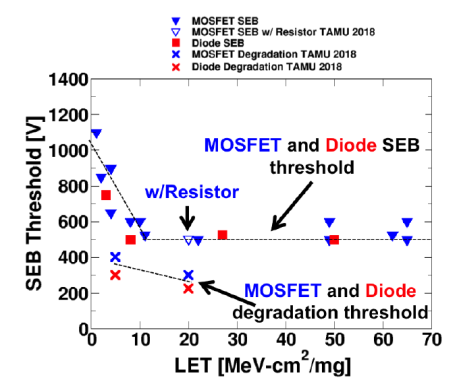
Figure 10. Relationship between bias voltage and heavy ion LET value for SEB of 1200V SiC MOSFET power devices and SiC diodes
The gate rupture effect in SiC MOSFET power devices occurs after heavy ion bombardment, where the electric field at the gate oxide is enhanced. When this electric field exceeds the critical breakdown field of the oxide, a single event gate rupture occurs. Figure 11 presents the results of TCAD simulations by Zhou X et al. [23] of the electric field distribution near the gate oxide after heavy ion bombardment of SiC MOSFET power devices. Figure 11(a) shows the structure of the device at the gate oxide position, and Figure 11(b) shows the electric field distribution on the gate oxide after the heavy ion bombardment. From the simulation results, it is observed that after the bombardment, a large electric field is generated near the gate oxide, with a peak electric field reaching 7MV/cm, which far exceeds the electric field threshold that the gate oxide can withstand. This large electric field peak is the primary cause of gate rupture.
|
|
(a) Ions attack the gate oxide position | (b) Gate oxide electric field distribution |
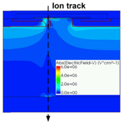
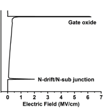
Figure 11. TCAD simulation of electric field distribution on the gate oxide after heavy ion attack on SiC MOSFET power devices
3. Wide bandgap power device applications in space solar power stations
3.1. Device-level radiation hardening
Total ionizing dose (TID) effects cause trap charges in the SiC MOSFET power device’s oxide layer, leading to degradation of the device’s electrical characteristics. To enhance the TID resistance of SiC MOSFETs, improvements can be made in the process to improve the quality of the oxide layer and reduce the area of the gate oxide. Based on the TID failure mechanism of the device, this paper proposes a segmented gate structure. By removing the gate oxide layer on the surface of the JFET region in the traditional VDMOS structure, the area of the gate oxide can be significantly reduced. When the device is exposed to radiation, the amount of charge accumulated in the gate oxide layer is drastically reduced, which helps improve the TID resistance of SiC MOSFETs, as shown in Figure 12. Figure 12(a) illustrates the structure without TID radiation hardening, and Figure 12(b) shows the segmented gate structure, which represents the radiation-hardened structure.
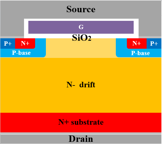
(a) (b)
Figure 12. Schematic cross-sectional view of (a) Un-hardened and (b) hardened SiC MOSFET power devices for TID
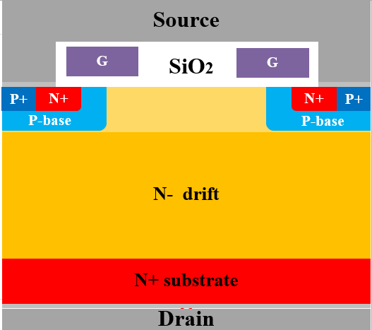
Single event gate rupture (SEGR) is a major failure issue in SiC MOSFET power devices. The failure mechanism primarily involves the generation of a large electric field at the gate oxide after heavy ion bombardment. This paper proposes a P+ field shielding structure, which significantly reduces the electric field intensity in the JFET region. This mitigates the effects of electron-hole pair accumulation near the gate oxide and the resulting electric field enhancement, thus improving the single event tolerance of SiC MOSFETs, as shown in Figure 13. Figure 13(a) illustrates the structure without SEGR hardening, and Figure 13(b) shows the electric field shielding hardening structure for single event gate rupture protection.

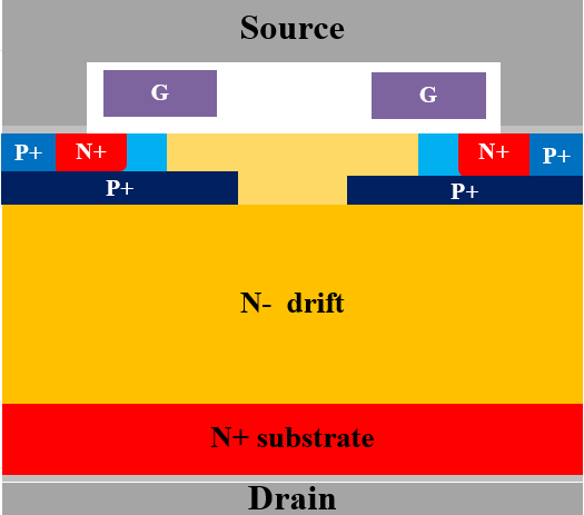
(a) (b)
Figure 13. Schematic cross-sectional view of (a) Un-hardened and (b) hardened SiC MOSFET power devices for SEGR
3.2. Circuit-level radiation hardening
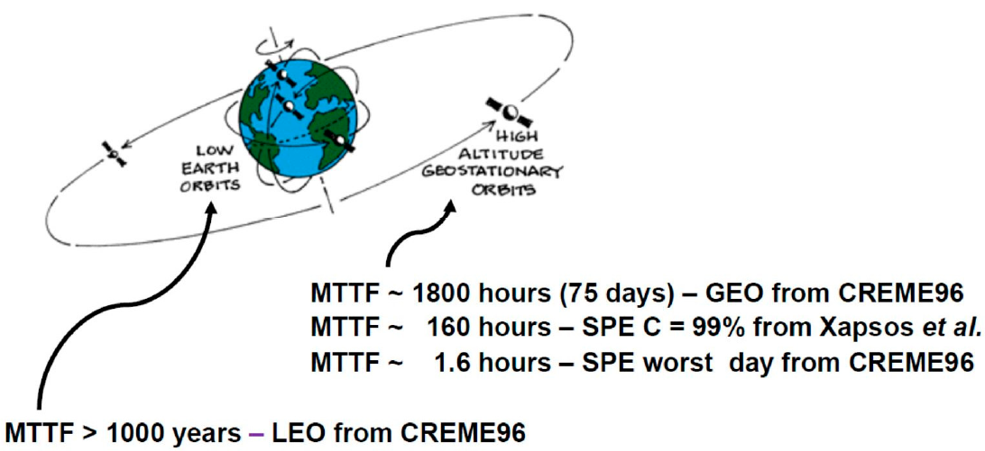
Figure 14. The working life of 1200V SiC MOSFET power devices in low Earth orbit (LEO) and geosynchronous equatorial orbit (GEO)
According to published literature, the maximum survival lifetime of 1200V SiC MOSFET power devices in LEO and GEO can reach up to 1000 years and 75 days, respectively, as shown in Figure 14 [24]. Based on this research, this section proposes a strategy to harden SiC MOSFET power devices against single event effects using a control algorithm, as shown in Figure 15. The FPGA control unit monitors the voltage and current of the SiC MOSFET power devices in use. If abnormal voltage or current is detected, the control unit assumes that the SiC MOSFET power device is being irradiated by radiation particles, and quickly switches to a backup SiC MOSFET power device to ensure the normal operation of the circuit.
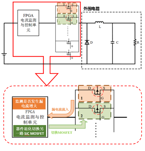
Figure 15. The schematic of the SEE hardened control algorithm.
Note: This image refers to the peripheral circuit and the FPGA current monitoring and control unit. The orange part represents the leakage current flowing in, monitoring whether the leakage current increases. The green part represents the switching of the MOSFET, where the device degradation triggers the switch to another SiC MOSFET.
4. Conclusion
This paper, in line with the practical needs of space solar power stations, examines the reliability, total ionizing dose, and single event failure issues of wide bandgap power devices in space solar power stations. It explores the feasibility of using wide bandgap power devices in space solar power stations. Based on the failure mechanisms of wide bandgap SiC MOSFET power devices, device-level and circuit-level radiation hardening methods have been proposed. These research results systematically summarize the challenges that wide bandgap power devices face in space solar power station applications and offer corresponding solutions, providing theoretical support for the rapid deployment of wide bandgap power devices in space solar power stations.
References
[1]. Shinohara, N. (2009). Recent wireless power transmission technologies in Japan for space solar power station/satellite. RWS, 13-15.
[2]. Matsumoto, H. (2002). Research on solar power satellites and microwave power transmission in Japan. IEEE Microwave Magazine, 36-45.
[3]. Han, Z. (2011). Introduction to radiation-resistant integrated circuits (pp. 1-12). Tsinghua University Press.
[4]. Liu, W. (2013). Radiation effects and reinforcement techniques for silicon semiconductor devices (pp. 1-6). Science Press.
[5]. Galloway, K. F. (2014). A brief review of heavy-ion radiation degradation and failure of silicon UMOS power transistors. Electronics, 3(4), 582-593.
[6]. George, J. S. (2019). An overview of radiation effects in electronics. AIP Conference Proceedings, 060002.
[7]. Adell, P., & Scheick, L. (2013). Radiation effects in power systems: A review. IEEE Transactions on Nuclear Science, 60(3), 1929-1952.
[8]. Lichtenwalner, D. J., Akturk, A., McGarrity, J., et al. (2018). Reliability of SiC power devices against cosmic ray neutron single-event burnout. Materials Science Forum, 559-562.
[9]. Sun, Y., Wan, X., Liu, Z., et al. (2022). Investigation of total ionizing dose effects in 4H-SiC power MOSFET under gamma ray radiation. Radiation Physics and Chemistry, 197, 110219.
[10]. Asai, H., Nashiyama, I., Sugimoto, K., et al. (2014). Tolerance against terrestrial neutron-induced single-event burnout in SiC MOSFETs. IEEE Transactions on Nuclear Science, 61(6), 3109-3114.
[11]. Tan, C. M., Pandey, V. K., Chiang, Y., et al. (2022). Electronic reliability analysis under radiation environment. Sensors and Materials: An International Journal on Sensor Technology, 3(3), 34.
[12]. Chbili, Z. (2015). Time-dependent dielectric breakdown in silicon carbide power MOSFETs.
[13]. Wang, L., Jia, Y., Zhou, X., et al. (2022). Degradation of 650 V SiC double-trench MOSFETs under repetitive overcurrent switching stress. Microelectronics and Reliability, 133(Jun.).
[14]. Envelope, J., Ad, A., Eb, A., et al. (2022). Benchmarking the robustness of Si and SiC MOSFETs: Unclamped inductive switching and short-circuit performance. Microelectronics Reliability.
[15]. Popelka, S., & Hazdra, P. (2016). Effect of electron irradiation on 1700V 4H-SiC MOSFET characteristics. Materials Science Forum, 856-859.
[16]. Yu, Q., Cao, S., Zhang, H., et al. (2019). Sensitivity analysis of single particle effects in SiC devices. Atomic Energy Science and Technology, 53(10), 2114-2119.
[17]. Lauenstein, J. M., Casey, M. C., Ladbury, R. L., et al. (2021). Space radiation effects on SiC power device reliability. In 2021 IEEE International Reliability Physics Symposium (IRPS), Monterey, CA, USA, 1-8.
[18]. Martinella, C., Ziemann, T., Stark, R., et al. (2020). Heavy-ion microbeam studies of single-event leakage current mechanism in SiC VD-MOSFETs. IEEE Transactions on Nuclear Science, 67(7), 1381-1389.
[19]. Waskiewicz, A. E., Groninger, J. W., Strahan, V. H., et al. (1986). Burnout of power MOS transistors with heavy ions of Californium-252. IEEE Transactions on Nuclear Science, 33(6), 1710-1713.
[20]. Lauenstein, J. M. (2018). Getting SiC power devices off the ground: Design, testing, and overcoming radiation threats. Microelectronics Reliability and Qualification Workshop (MRQW), El Segundo, CA. Retrieved from https://aerospace.org/MRQW
[21]. Ball, D. R., Galloway, K. F., Johnson, R. A., et al. (2020). Ion-induced energy pulse mechanism for single-event burnout in high-voltage SiC power MOSFETs and junction barrier Schottky diodes. IEEE Transactions on Nuclear Science, 67(1), 22-28.
[22]. Tang, Z. H., Li, X. J., Tan, K. Z., et al. (2018). The progress of SEB and SEGR irradiation hardening technology for power MOSFET. In 2018 European Conference on Radiation and its Effects on Components and Systems (RADECS), Gothenburg, Sweden, September 2018.
[23]. Zhou, X., Pang, H., Jia, Y., et al. (2021). Gate oxide damage of SiC MOSFETs induced by heavy-ion strike. IEEE Transactions on Electron Devices, 68(8), 4010-4015.
[24]. Kenneth, G., Arthur, W., Ronald, S., et al. (2018). Failure estimates for SiC power MOSFETs in space electronics. Aerospace, 5(3), 1-7.
Cite this article
Wang,M.;Zhao,S.;Li,Y.;Li,Z.;Zhang,L. (2025). Feasibility study of wide bandgap power devices in space solar power station applications. Advances in Engineering Innovation,16(1),28-35.
Data availability
The datasets used and/or analyzed during the current study will be available from the authors upon reasonable request.
Disclaimer/Publisher's Note
The statements, opinions and data contained in all publications are solely those of the individual author(s) and contributor(s) and not of EWA Publishing and/or the editor(s). EWA Publishing and/or the editor(s) disclaim responsibility for any injury to people or property resulting from any ideas, methods, instructions or products referred to in the content.
About volume
Journal:Advances in Engineering Innovation
© 2024 by the author(s). Licensee EWA Publishing, Oxford, UK. This article is an open access article distributed under the terms and
conditions of the Creative Commons Attribution (CC BY) license. Authors who
publish this series agree to the following terms:
1. Authors retain copyright and grant the series right of first publication with the work simultaneously licensed under a Creative Commons
Attribution License that allows others to share the work with an acknowledgment of the work's authorship and initial publication in this
series.
2. Authors are able to enter into separate, additional contractual arrangements for the non-exclusive distribution of the series's published
version of the work (e.g., post it to an institutional repository or publish it in a book), with an acknowledgment of its initial
publication in this series.
3. Authors are permitted and encouraged to post their work online (e.g., in institutional repositories or on their website) prior to and
during the submission process, as it can lead to productive exchanges, as well as earlier and greater citation of published work (See
Open access policy for details).
References
[1]. Shinohara, N. (2009). Recent wireless power transmission technologies in Japan for space solar power station/satellite. RWS, 13-15.
[2]. Matsumoto, H. (2002). Research on solar power satellites and microwave power transmission in Japan. IEEE Microwave Magazine, 36-45.
[3]. Han, Z. (2011). Introduction to radiation-resistant integrated circuits (pp. 1-12). Tsinghua University Press.
[4]. Liu, W. (2013). Radiation effects and reinforcement techniques for silicon semiconductor devices (pp. 1-6). Science Press.
[5]. Galloway, K. F. (2014). A brief review of heavy-ion radiation degradation and failure of silicon UMOS power transistors. Electronics, 3(4), 582-593.
[6]. George, J. S. (2019). An overview of radiation effects in electronics. AIP Conference Proceedings, 060002.
[7]. Adell, P., & Scheick, L. (2013). Radiation effects in power systems: A review. IEEE Transactions on Nuclear Science, 60(3), 1929-1952.
[8]. Lichtenwalner, D. J., Akturk, A., McGarrity, J., et al. (2018). Reliability of SiC power devices against cosmic ray neutron single-event burnout. Materials Science Forum, 559-562.
[9]. Sun, Y., Wan, X., Liu, Z., et al. (2022). Investigation of total ionizing dose effects in 4H-SiC power MOSFET under gamma ray radiation. Radiation Physics and Chemistry, 197, 110219.
[10]. Asai, H., Nashiyama, I., Sugimoto, K., et al. (2014). Tolerance against terrestrial neutron-induced single-event burnout in SiC MOSFETs. IEEE Transactions on Nuclear Science, 61(6), 3109-3114.
[11]. Tan, C. M., Pandey, V. K., Chiang, Y., et al. (2022). Electronic reliability analysis under radiation environment. Sensors and Materials: An International Journal on Sensor Technology, 3(3), 34.
[12]. Chbili, Z. (2015). Time-dependent dielectric breakdown in silicon carbide power MOSFETs.
[13]. Wang, L., Jia, Y., Zhou, X., et al. (2022). Degradation of 650 V SiC double-trench MOSFETs under repetitive overcurrent switching stress. Microelectronics and Reliability, 133(Jun.).
[14]. Envelope, J., Ad, A., Eb, A., et al. (2022). Benchmarking the robustness of Si and SiC MOSFETs: Unclamped inductive switching and short-circuit performance. Microelectronics Reliability.
[15]. Popelka, S., & Hazdra, P. (2016). Effect of electron irradiation on 1700V 4H-SiC MOSFET characteristics. Materials Science Forum, 856-859.
[16]. Yu, Q., Cao, S., Zhang, H., et al. (2019). Sensitivity analysis of single particle effects in SiC devices. Atomic Energy Science and Technology, 53(10), 2114-2119.
[17]. Lauenstein, J. M., Casey, M. C., Ladbury, R. L., et al. (2021). Space radiation effects on SiC power device reliability. In 2021 IEEE International Reliability Physics Symposium (IRPS), Monterey, CA, USA, 1-8.
[18]. Martinella, C., Ziemann, T., Stark, R., et al. (2020). Heavy-ion microbeam studies of single-event leakage current mechanism in SiC VD-MOSFETs. IEEE Transactions on Nuclear Science, 67(7), 1381-1389.
[19]. Waskiewicz, A. E., Groninger, J. W., Strahan, V. H., et al. (1986). Burnout of power MOS transistors with heavy ions of Californium-252. IEEE Transactions on Nuclear Science, 33(6), 1710-1713.
[20]. Lauenstein, J. M. (2018). Getting SiC power devices off the ground: Design, testing, and overcoming radiation threats. Microelectronics Reliability and Qualification Workshop (MRQW), El Segundo, CA. Retrieved from https://aerospace.org/MRQW
[21]. Ball, D. R., Galloway, K. F., Johnson, R. A., et al. (2020). Ion-induced energy pulse mechanism for single-event burnout in high-voltage SiC power MOSFETs and junction barrier Schottky diodes. IEEE Transactions on Nuclear Science, 67(1), 22-28.
[22]. Tang, Z. H., Li, X. J., Tan, K. Z., et al. (2018). The progress of SEB and SEGR irradiation hardening technology for power MOSFET. In 2018 European Conference on Radiation and its Effects on Components and Systems (RADECS), Gothenburg, Sweden, September 2018.
[23]. Zhou, X., Pang, H., Jia, Y., et al. (2021). Gate oxide damage of SiC MOSFETs induced by heavy-ion strike. IEEE Transactions on Electron Devices, 68(8), 4010-4015.
[24]. Kenneth, G., Arthur, W., Ronald, S., et al. (2018). Failure estimates for SiC power MOSFETs in space electronics. Aerospace, 5(3), 1-7.