


1. Introduction
Two-dimensional materials refer to materials with one dimension significantly reduced—typically at the nanoscale, with a thickness of only a few atomic or molecular layers—while the other two dimensions extend substantially in space. These materials exhibit unique physical properties. Their distinctive electronic structures grant them immense potential in the field of electronic devices; their outstanding mechanical properties suggest promising applications in composite materials; and their special optical characteristics hold the potential to transform the field of optoelectronics. Two-dimensional semiconductor materials represent a key subcategory of 2D materials. In addition to the general traits shared by 2D materials, they also possess specific semiconductor properties, such as high carrier mobility, excellent gate controllability, and efficient suppression of short-channel effects. Since their discovery, 2D semiconductor materials have attracted extensive research interest. Their development holds great significance for the advancement of integrated circuits and microelectronic devices.
2. Introduction to Two-Dimensional materials
Two-Dimensional (2D) materials are a class of materials with a distinctive structural configuration, characterized by having one dimension that is extremely small in the three-dimensional space, while the other two dimensions are relatively large—typically differing by about six orders of magnitude. These materials can be regarded as planar structures composed of single or multiple layers of atoms or molecules.
The study of 2D materials first attracted the attention of scientists as early as the beginning of the twentieth century. However, it was not until 2004 that they gained widespread recognition, when A. Geim and K. Novoselov successfully isolated graphene from graphite using the tape exfoliation method [1]. Graphene’s exceptional electrical and thermal conductivity, high strength and flexibility, and unique light absorption and emission properties quickly made it a rising star in materials research. Since then, scientists have synthesized many other 2D materials with distinctive properties, as illustrated in Figure 1. These include elemental 2D materials (e.g., silicene, germanene, phosphorene) [2-4]; 2D boron-carbon-nitrogen compounds (e.g., h-BN, g-C₃N₄) [5, 6]; transition metal dichalcogenides (TMDs, such as MoS₂, TaS₂) [7-9]; noble metal dichalcogenides (NMDs, such as PtS₂, PdSe₂) [10]; 2D transition metal carbides/nitrides (MXenes, such as Fe₂C, MoN₂) [10]; and 2D transition metal halides (e.g., CrI₃, VCl₃) [11,12].
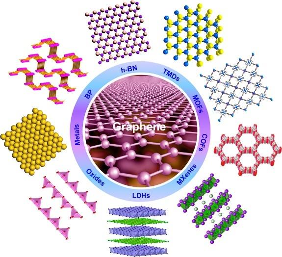
Figure 1. Types of Two-Dimensional materials and their crystal structures [6]
3. Several typical Two-Dimensional materials
Due to their unique crystal structures, Two-Dimensional (2D) materials occupy a special position in the field of optoelectronics. As research into these materials continues to deepen, scientists aim to explore methods that enhance their advantages in practical applications. Currently, the most representative 2D semiconductor materials include graphene, hexagonal boron nitride, two-dimensional transition metal dichalcogenides, and phosphorene.
3.1. Graphene
In 2004, scientists Andre Geim and Konstantin Novoselov successfully isolated graphene from graphite using the method of micromechanical exfoliation. This form of graphene remains the thinnest 2D material discovered to date. In graphene, each carbon atom forms three σ-bonds with three adjacent carbon atoms, creating a hexagonal ring structure, as shown in Figure 2(a). Additionally, the p-orbitals of carbon atoms overlap with those of adjacent atoms to form π-bonds. This tightly bonded σ-π configuration gives graphene its extraordinary stability and unique electronic properties [13]. Owing to the distinct crystal structure and bonding of graphene, it possesses a special electronic band structure, as shown in Figure 2(c). Near the special K-points in the Brillouin zone, the band structure of graphene forms Dirac points. Around these points, electrons and holes exhibit high mobility, resulting in high carrier mobility in graphene even at room temperature.
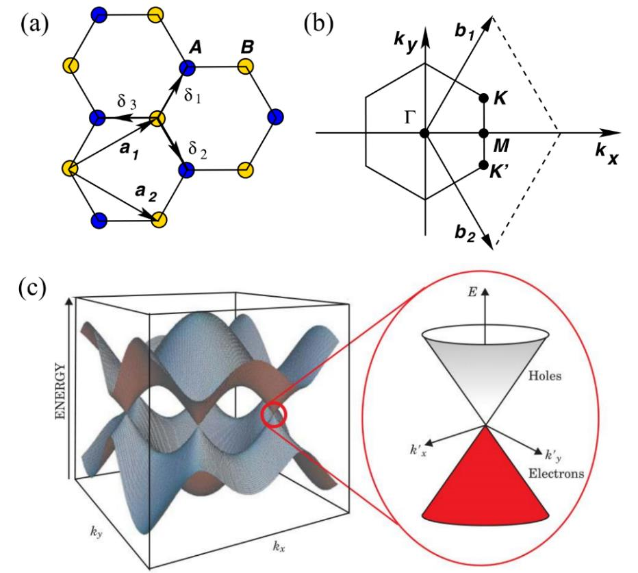
Figure 2. (a) Hexagonal lattice structure of graphene, (b) brillouin zone corresponding to the lattice, (c) band structure and magnified view of the dirac cone [14]
3.2. Hexagonal boron nitride
Hexagonal Boron Nitride (h-BN) is the most common and stable 2D crystalline form among the four known boron nitride compounds [15]. As shown in Figure 3, its crystal and band structures are similar to those of graphene; however, the bandgap differs, resulting in distinct physical and chemical properties. h-BN exhibits excellent thermal stability and thermal conductivity, and it remains stable under high-temperature conditions. These outstanding properties offer significant potential for industrial applications.
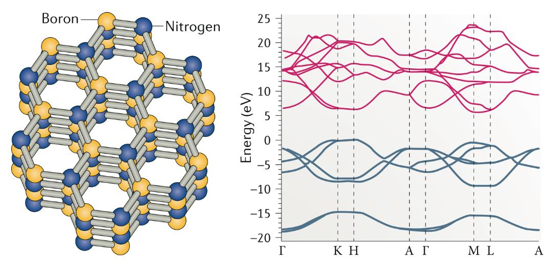
Figure 3. h-BN and its band structure [15]
3.3. Two-Dimensional transition metal dichalcogenides
Two-Dimensional Transition Metal Dichalcogenides (TMDs), with the general chemical formula MX₂ (where M is a transition metal such as Ti, Mo, or W, and X is a chalcogen element such as S, Se, or Te) [16-19], can be categorized into hexagonal and trigonal crystal structures depending on their atomic arrangement. The crystal structures of some TMDs are shown in Figure 4. The electronic band structures of TMDs vary significantly, leading to different physical properties depending on the elemental composition. Monolayer MoS₂, for instance, demonstrates strong thermal stability and high carrier mobility at room temperature, making it a promising material in the field of electronics.
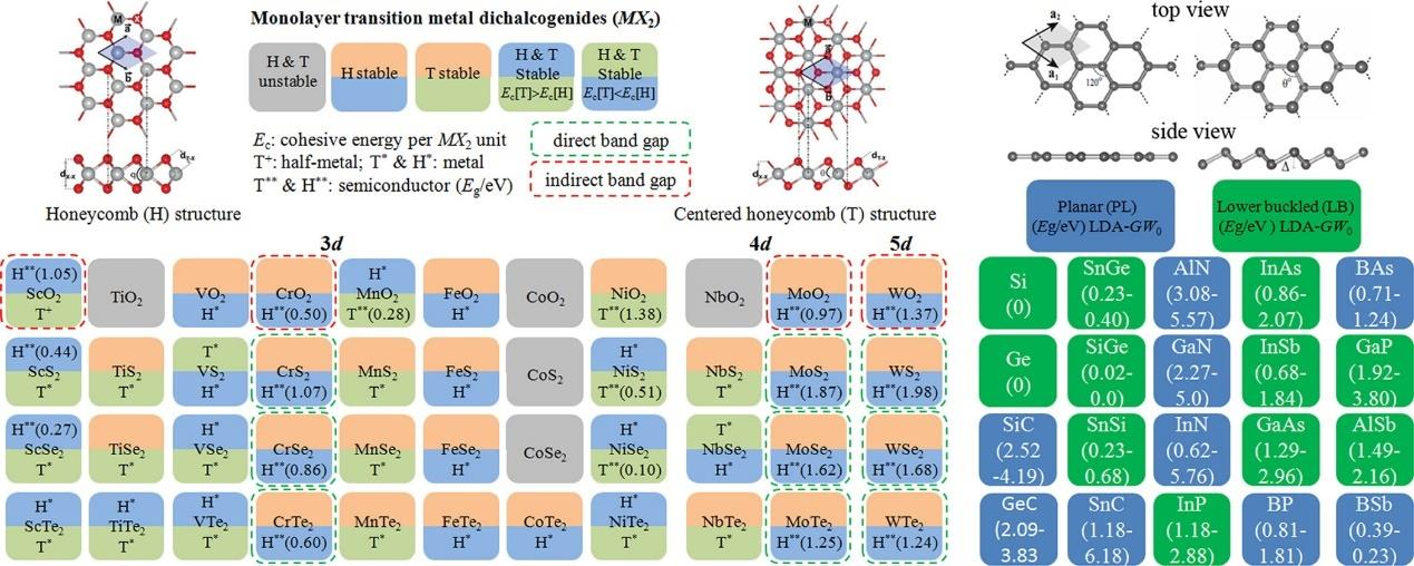
Figure 4. Crystal structures, physical properties, and stability of selected TMDs [19]
3.4. Phosphorene
Phosphorene exists in several allotropes, among which the most representative are black phosphorene with an orthorhombic structure and blue phosphorene with a honeycomb structure, as shown in Figure 5. The electronic structure of black phosphorene was first proposed in 1953. Its layers are held together by van der Waals forces, while the atoms within each monolayer are covalently bonded. In 2014, Professor Zhang and Professor Chen’s team successfully obtained monolayer black phosphorene via mechanical exfoliation. Research on black phosphorene indicates that it is a direct bandgap semiconductor and exhibits anisotropic properties. This unique structure distinguishes it from other Two-Dimensional semiconductor materials. In contrast, blue phosphorene is an indirect bandgap semiconductor.
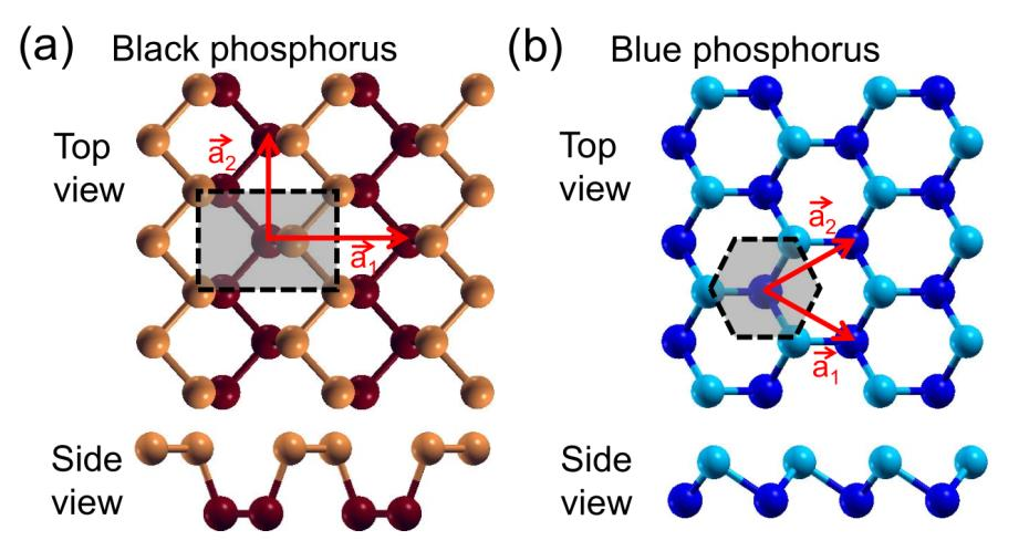
Figure 5. (a) Structure of black phosphorene (b) structure of blue phosphorene [20]
4. Applications of Two-Dimensional materials
4.1. Electronic and optoelectronic devices
Over the past few decades, three-dimensional materials have dominated the field. However, as technology has advanced, the scale requirements for electronic devices have become increasingly stringent, pushing three-dimensional materials closer to their physical limits. To enable further technological progress, the discovery of novel materials has become imperative. Researchers have found that Two-Dimensional (2D) materials show great promise in breaking through these limitations.
As shown in Figure 5, 2D materials exhibit broad application prospects in electronic and optoelectronic devices. They can be utilized in the development of long-wavelength photodetectors to capture light signals across different spectral bands; 2D polarized materials used in photodetectors can enhance sensitivity through anisotropy; 2D materials employed in photonic memory devices enable low-power information storage and processing; and their application in optical modulators allows for the regulation and control of light signals, providing more efficient solutions for optical communication. Furthermore, 2D materials are widely used in other electronic components—for example, heterojunctions formed by monolayer MoS₂ in contact with conductive graphene, and back-gate field-effect transistors fabricated using monolayer Black Phosphorus (BP).
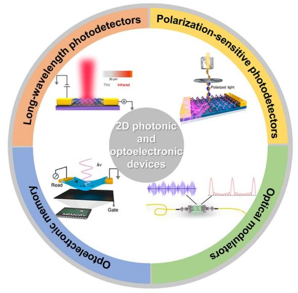
Figure 6. Applications of Two-Dimensional materials in optoelectronic devices [21]
4.2. Rechargeable batteries
Rechargeable batteries are power sources that can restore electrical energy through reversible electrochemical reactions. Widely used in everyday life, they are closely tied to various aspects of modern living. Compared to disposable batteries, rechargeable batteries offer reusability, greater environmental friendliness, and better economic value, aligning more closely with daily needs. However, performance degradation over time, long charging durations, and potential safety risks remain significant challenges. The development of novel batteries using 2D materials may offer solutions to these issues.
When used as intercalation-type electrodes, 2D materials allow for reduced intercalation resistance and lower energy loss through rational structural design, thereby improving cycling performance. Additionally, their unique crystal structures endow them with excellent mechanical adaptability during long-term cycling, allowing them to withstand strain and stress in the electrode matrix.
The diversity of 2D materials has also spurred the development of heterostructures in rechargeable batteries, which are generally classified into two categories: van der Waals heterostructures composed of stacked 2D materials and mixed-dimensional heterostructures. Designing these heterostructures can enhance both physical and chemical properties of the materials. Consequently, 2D heterostructures have been widely applied in energy storage devices such as redox materials, support frameworks, active material hosts, separators, and catalysts [22-24].
4.3. Supercapacitors
Supercapacitors are electronic components capable of rapidly storing and releasing electrical energy. Compared to traditional batteries, they offer faster charge–discharge rates and higher power density.
2D materials possess immense potential in supercapacitor applications due to their distinctive properties. Their high specific surface area provides ample charge storage sites, thereby increasing energy and power density. Their unique crystal structures and electronic characteristics allow for greater charge storage capacity, enhancing energy storage. Their superior electron transport and ion diffusion efficiencies enable rapid charging and discharging. Additionally, the physical and chemical stability of 2D materials extends the service life of supercapacitors. Their structural tunability makes them adaptable to various application scenarios. Finally, with thicknesses down to just a few atoms, 2D materials can reduce the mass of supercapacitors, making them suitable for broader applications.
Extensive research has already been conducted on the application of 2D materials in supercapacitors. For instance, Gao et al. developed a novel all-solid-state asymmetric supercapacitor using monolayer β-Co(OH)₂ as the cathode and n-type doped graphene as the anode. This device delivered an operating voltage of 1.8 V, ultra-high energy and power density, and maintained 93.2% capacitance retention after 10,000 cycles [25]. Li et al. introduced mesopores into a 2D metal–organic framework (MOF) heterostructure, creating a hierarchical porous Zn-MOF hybrid structure. At a current density of 0.2 A·g⁻¹, the Meso-Zn-MOF@rGO-PBA achieved a specific capacitance of 292.8 F·g⁻¹—10.3 times higher than that of pure Zn-MOF (26 F·g⁻¹)—and retained 83.2% of its capacitance after 2,000 cycles [26].
4.4. Solar cells
Compared with conventional materials, 2D materials offer tremendous potential in solar cell applications, owing to several advantages. Their strong light absorption capacity allows them to capture visible and infrared light across multiple wavelengths, thereby improving absorption and conversion efficiency. Some 2D materials also exhibit excellent flexibility, enabling the fabrication of flexible solar cells suitable for a wide range of applications. Their layered structure and high crystallographic orientation allow efficient charge carrier transport, contributing to higher conversion efficiencies. Doping of 2D materials can tailor their band structures, enhancing the stability of solar cells. Additionally, 2D materials can be produced on a large scale using low-cost methods such as mechanical exfoliation, reducing manufacturing costs.
As shown in Figure 7, materials such as graphene, BP, MXenes, and transition metal sulfides have been widely applied in the solar cell field, leading to the development of various solar cell types. Currently, the highest power conversion efficiencies are observed in graphene-, perovskite-, and nano-silicon-based solar cells [27]. Zhang et al. reported a graphene-based solar cell with a modular structural design, achieving a power conversion efficiency of 18.65%, among the highest for carbon-based solar cells [28].
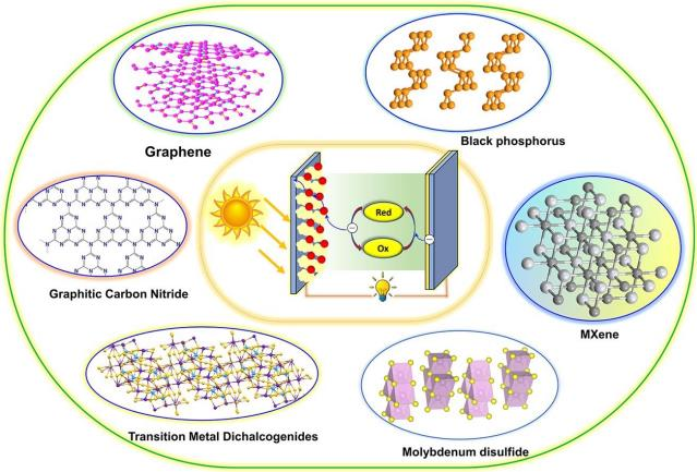
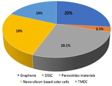
Figure 7. (a) Schematic diagram of 2D materials in solar cells (b) conversion efficiencies of solar cells based on various 2D materials [29, 30]
4.5. Photocatalysis
Photocatalysis is a technology that uses light to promote chemical reactions by converting light energy into chemical energy. A catalyst is usually required to facilitate specific reactions. As shown in Figure 8, the photocatalytic process generally consists of three key steps: first, upon illumination, electrons in the material are excited to generate electron–hole pairs. These pairs then separate and migrate along different paths either within or on the surface of the material, a critical step for initiating photocatalytic reactions. Next, the separated excited electrons and holes participate in surface chemical reactions. Finally, the reaction products desorb from the surface, allowing the catalyst to continue participating in subsequent reactions. Maintaining surface activity by ensuring timely desorption of products is essential for sustained catalytic performance.
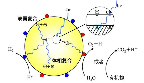
Figure 8. Schematic diagram of the photocatalytic process in materials [31]
Compared to traditional catalysts, 2D photocatalytic materials offer several advantages. Their large specific surface area provides more active sites for catalysis, enhancing reaction efficiency. Their superior optical properties enable absorption of multiple light wavelengths and improve electron excitation efficiency. The electronic structures of 2D materials can be modulated via chemical modifications or external fields, enabling precise control over different catalytic reactions. Their unique crystal structures also facilitate efficient charge carrier transport, reducing recombination rates and increasing photocatalytic performance. These characteristics make 2D materials uniquely suited for photocatalytic applications.
Discovering new 2D photocatalysts has become a key research focus in the field. For example, Tian et al. prepared a Bi₂MoO₆ nanosheet/TiO₂ nanobelt hybrid composite for photocatalytic oxygen generation [32]. Zhou et al. pointed out that MoS₂ nanosheets are excellent co-catalysts for TiO₂-based photocatalytic hydrogen production [33].
5. Conclusion
Owing to their unique crystal structures and electronic properties, 2D materials have emerged as a focal point of scientific research in the 21st century. Since A. Geim and K. Novoselov successfully exfoliated graphene using adhesive tape in 2004, numerous 2D materials such as hexagonal boron nitride, transition metal dichalcogenides, and phosphorene have been discovered, continuously expanding the 2D material family. Ongoing research into 2D materials is expected to overcome the limitations of traditional materials in electronic devices, enable the development of safer and longer-lasting batteries, higher-capacity supercapacitors, and more efficient catalytic processes. The study of 2D materials is of profound scientific significance and far-reaching impact.
References
[1]. Novoselov, K. S., Geim, A. K., Morozov, S. V., Jiang, D., Zhang, Y., Dubonos, S. V., Grigorieva, I. V., & Firsov, A. A. (2004). Electric field effect in atomically thin carbon films. Science, 306(5696), 666–669.
[2]. Mannix, A. J., Zhou, Z., Kiraly, B., Wood, J. D., Alducin, D., Myers, B. D., ... & Hersam, M. C. (2018). Borophene as a prototype for synthetic 2D materials development. Nature Nanotechnology, 13(6), 444–450.
[3]. Li, L., Yu, Y., Ye, G. J., Ge, Q., Ou, X., Wu, H., Feng, D., Chen, X. H., & Zhang, Y. (2014). Black phosphorus field-effect transistors. Nature Nanotechnology, 9(5), 372–377.
[4]. Bafekry, A., Yagmurcukardes, M., Akgenc, B., Ghergherehchi, M., & Nguyen, C. V. (2020). Van der Waals heterostructures of MoS₂ and Janus MoSSe monolayers on graphitic boron. Journal of Physics D: Applied Physics, 53(35). 10.1088/1361-6463/ab876c
[5]. Caldwell, J. D., Aharonovich, I., Cassabois, G., Edgar, J. H., Gil, B., & Basov, D. N. (2019). Photonics with hexagonal boron nitride. Nature Reviews Materials, 4(8), 552–567.
[6]. Zhang, H. (2015). Ultrathin two-dimensional nanomaterials. ACS Nano, 9(10), 9451-9469. DOI: 10.1021/acsnano.5b05040
[7]. Lee, J., Bang, J., & Kang, J. (2022). Nonequilibrium charge-density-wave melting in 1T-TaS₂ triggered by electronic excitation: A real-time time-dependent density functional theory study. The Journal of Physical Chemistry Letters, 13(25), 5711–5718.
[8]. Huang, H., Zha, J., Li, S., Wang, Y., & Zhang, C. (2022). Two-dimensional alloyed transition metal dichalcogenide nanosheets: Synthesis and applications. Chinese Chemical Letters, 33(1), 163–176.
[9]. Zhao, Y., Zhu, L., Zhou, B., & Jiang, S. (2023). Chemical vapor deposition of uniform bilayer PtS₂ flakes for electrocatalytic hydrogen evolution. Physical Chemistry Chemical Physics, 25(16), 11311-11315. doi: 10.1039/d3cp01164j
[10]. Hu, Y., Liu, X. Y., Shen, Z. H., Luo, Z. F., Chen, Z. G., & Fan, X. L. (2020). High Curie temperature and carrier mobility of novel Fe, Co and Ni carbide MXenes. Nanoscale, 12(21), 11627–11637.
[11]. Gibertini, M., Koperski, M., Morpurgo, A. F., & Novoselov, K. S. (2019). Magnetic 2D materials and heterostructures. Nature Nanotechnology, 14(5), 408–419.
[12]. Zhao, S., Wan, W., Ge, Y., & Liu, Y. (2021). Prediction of chalcogen-doped VCl₃ monolayers as 2D ferromagnetic semiconductors with enhanced optical absorption. Annalen der Physik, 533(6). https://doi.org/10.1002/andp.202100064
[13]. Castro Neto, A. H., Guinea, F., Peres, N. M. R., & Geim, A. K. (2009). The electronic properties of graphene. Reviews of Modern Physics, 81(1), 109–162.
[14]. Das Sarma, S., Adam, S., Hwang, E. H., & Rossi, E. (2011). Electronic transport in two-dimensional graphene. Reviews of Modern Physics, 83(2), 407–470.
[15]. Bhimanapati, G. R., Kozuch, D., & Robinson, J. A. (2014). Large-scale synthesis and functionalization of hexagonal boron nitride nanosheets. Nanoscale, 6(20), 11671–11675.
[16]. Chen, J., Wu, K., Ma, H., Hu, W., & Yang, J. (2020). Tunable Rashba spin splitting in Janus transition-metal dichalcogenide monolayers via charge doping. RSC Advances, 10(11), 6388–6394.
[17]. Zhang, Q., Dong, S., Cao, G., & Hu, G. (2020). Exciton polaritons in mixed-dimensional transition metal dichalcogenides heterostructures. Optics Letters, 45(15), 4140–4143.
[18]. Zhou, W., Gong, H., Jin, X., Chen, Y., Li, H., & Liu, S. (2022). Recent progress of two-dimensional transition metal dichalcogenides for thermoelectric applications. Frontiers in Physics, 10. https://doi.org/10.3389/fphy.2022.842789
[19]. Yin, X., Tang, C. S., Zheng, Y., Gao, J., Wu, J., Zhang, H., ... & Wee, A. T. S. (2021). Recent developments in 2D transition metal dichalcogenides: Phase transition and applications of the (quasi-)metallic phases. Chemical Society Reviews, 50(18), 10087-10115.
[20]. Zhu, Z., & Tománek, D. (2014). Semiconducting layered blue phosphorus: A computational study. Physical Review Letters, 112(17), 176802.
[21]. Wang, X., Cui, Y., Li, T., Lei, M., Li, J., & Wei, Z. (2019). Recent advances in the functional 2D photonic and optoelectronic devices. Advanced Optical Materials, 7(3). DOI: 10.1002/adom.201801274
[22]. Augustyn, V., & Gogotsi, Y. (2017). 2D materials with nanoconfined fluids for electrochemical energy storage. Joule, 1(3), 443–452.
[23]. Wan, J., Lacey, S. D., Dai, J., Bao, W., Fuhrer, M. S., & Hu, L. (2016). Tuning two-dimensional nanomaterials by intercalation: Materials, properties and applications. Chemical Society Reviews, 45(24), 6742–6765.
[24]. Yan, C., Fang, Z., Lv, C., Zhou, X., Chen, G., & Yu, G. (2018). Significantly improving lithium-ion transport via conjugated anion intercalation in inorganic layered hosts. ACS Nano, 12(8), 8670–8677.
[25]. Gao, S., Sun, Y., Lei, F., Liang, L., Liu, J., Bi, W., ...& Xie, Y. (2014). Ultrahigh energy density realized by a single-layer β-Co(OH)₂ all-solid-state asymmetric supercapacitor. Angewandte Chemie International Edition, 53(47), 12789–12793.
[26]. Li, S., Zhang, Y., Cheng, Q., Ye, P., Shen, X., Nie, Y., & Li, L. (2023). Construction of hierarchical porous two-dimensional Zn-MOF-based heterostructures for supercapacitor applications. Journal of Alloys and Compounds, 968. https://doi.org/10.1016/j.jallcom.2023.171971
[27]. Kumar, K. S., Choudhary, N., Jung, Y., & Thomas, J. (2018). Recent advances in two-dimensional nanomaterials for supercapacitor electrode applications. ACS Energy Letters, 3(2), 482–495.
[28]. Zhang, C., Wang, S., Zhang, H., Feng, Y., Tian, W., Yan, Y., ... &Shi, Y. (2019). Efficient stable graphene-based perovskite solar cells with high flexibility in device assembling via modular architecture design. Energy & Environmental Science. 12, 3585-3594.
[29]. Iqbal, T., Fatima, S., Bibi, T., & Zafar, M. (2021). Graphene and other two-dimensional materials in advanced solar cells. Optical and Quantum Electronics, 53(5). https://doi.org/10.1007/s11082-021-02852-9
[30]. Kumar, S., Kumar, S., Rai, R. N., Lee, Y., Nguyen Thi, H. C., Kim, S. Y., ... Singh, L. (2023). Recent development in two-dimensional material-based advanced photoanodes for high-performance dye-sensitized solar cells. Solar Energy, 249, 606–623.
[31]. Wang, H., Zhang, X., & Xie, Y. (2018). Recent progress in ultrathin two-dimensional semiconductors for photocatalysis. Materials Science and Engineering: R: Reports, 130, 1–39.
[32]. Tian, J., Hao, P., Wei, N., Cui, H., & Liu, H. (2015). 3D Bi₂MoO₆ nanosheet/TiO₂ nanobelt heterostructure: Enhanced photocatalytic activities and photoelectrochemistry performance. ACS Catalysis, 5(8), 4530–4536.
[33]. Zhou, W., Yin, Z., Du, Y., Huang, X., Zeng, Z., Fan, Z., ... Zhang, H. (2013). Synthesis of few-layer MoS₂ nanosheet-coated TiO₂ nanobelt heterostructures for enhanced photocatalytic activities. Small, 9(1), 140–147.
Cite this article
Li,Y. (2025). A review of research on Two-Dimensional semiconductor materials. Advances in Engineering Innovation,16(6),117-123.
Data availability
The datasets used and/or analyzed during the current study will be available from the authors upon reasonable request.
Disclaimer/Publisher's Note
The statements, opinions and data contained in all publications are solely those of the individual author(s) and contributor(s) and not of EWA Publishing and/or the editor(s). EWA Publishing and/or the editor(s) disclaim responsibility for any injury to people or property resulting from any ideas, methods, instructions or products referred to in the content.
About volume
Journal:Advances in Engineering Innovation
© 2024 by the author(s). Licensee EWA Publishing, Oxford, UK. This article is an open access article distributed under the terms and
conditions of the Creative Commons Attribution (CC BY) license. Authors who
publish this series agree to the following terms:
1. Authors retain copyright and grant the series right of first publication with the work simultaneously licensed under a Creative Commons
Attribution License that allows others to share the work with an acknowledgment of the work's authorship and initial publication in this
series.
2. Authors are able to enter into separate, additional contractual arrangements for the non-exclusive distribution of the series's published
version of the work (e.g., post it to an institutional repository or publish it in a book), with an acknowledgment of its initial
publication in this series.
3. Authors are permitted and encouraged to post their work online (e.g., in institutional repositories or on their website) prior to and
during the submission process, as it can lead to productive exchanges, as well as earlier and greater citation of published work (See
Open access policy for details).
References
[1]. Novoselov, K. S., Geim, A. K., Morozov, S. V., Jiang, D., Zhang, Y., Dubonos, S. V., Grigorieva, I. V., & Firsov, A. A. (2004). Electric field effect in atomically thin carbon films. Science, 306(5696), 666–669.
[2]. Mannix, A. J., Zhou, Z., Kiraly, B., Wood, J. D., Alducin, D., Myers, B. D., ... & Hersam, M. C. (2018). Borophene as a prototype for synthetic 2D materials development. Nature Nanotechnology, 13(6), 444–450.
[3]. Li, L., Yu, Y., Ye, G. J., Ge, Q., Ou, X., Wu, H., Feng, D., Chen, X. H., & Zhang, Y. (2014). Black phosphorus field-effect transistors. Nature Nanotechnology, 9(5), 372–377.
[4]. Bafekry, A., Yagmurcukardes, M., Akgenc, B., Ghergherehchi, M., & Nguyen, C. V. (2020). Van der Waals heterostructures of MoS₂ and Janus MoSSe monolayers on graphitic boron. Journal of Physics D: Applied Physics, 53(35). 10.1088/1361-6463/ab876c
[5]. Caldwell, J. D., Aharonovich, I., Cassabois, G., Edgar, J. H., Gil, B., & Basov, D. N. (2019). Photonics with hexagonal boron nitride. Nature Reviews Materials, 4(8), 552–567.
[6]. Zhang, H. (2015). Ultrathin two-dimensional nanomaterials. ACS Nano, 9(10), 9451-9469. DOI: 10.1021/acsnano.5b05040
[7]. Lee, J., Bang, J., & Kang, J. (2022). Nonequilibrium charge-density-wave melting in 1T-TaS₂ triggered by electronic excitation: A real-time time-dependent density functional theory study. The Journal of Physical Chemistry Letters, 13(25), 5711–5718.
[8]. Huang, H., Zha, J., Li, S., Wang, Y., & Zhang, C. (2022). Two-dimensional alloyed transition metal dichalcogenide nanosheets: Synthesis and applications. Chinese Chemical Letters, 33(1), 163–176.
[9]. Zhao, Y., Zhu, L., Zhou, B., & Jiang, S. (2023). Chemical vapor deposition of uniform bilayer PtS₂ flakes for electrocatalytic hydrogen evolution. Physical Chemistry Chemical Physics, 25(16), 11311-11315. doi: 10.1039/d3cp01164j
[10]. Hu, Y., Liu, X. Y., Shen, Z. H., Luo, Z. F., Chen, Z. G., & Fan, X. L. (2020). High Curie temperature and carrier mobility of novel Fe, Co and Ni carbide MXenes. Nanoscale, 12(21), 11627–11637.
[11]. Gibertini, M., Koperski, M., Morpurgo, A. F., & Novoselov, K. S. (2019). Magnetic 2D materials and heterostructures. Nature Nanotechnology, 14(5), 408–419.
[12]. Zhao, S., Wan, W., Ge, Y., & Liu, Y. (2021). Prediction of chalcogen-doped VCl₃ monolayers as 2D ferromagnetic semiconductors with enhanced optical absorption. Annalen der Physik, 533(6). https://doi.org/10.1002/andp.202100064
[13]. Castro Neto, A. H., Guinea, F., Peres, N. M. R., & Geim, A. K. (2009). The electronic properties of graphene. Reviews of Modern Physics, 81(1), 109–162.
[14]. Das Sarma, S., Adam, S., Hwang, E. H., & Rossi, E. (2011). Electronic transport in two-dimensional graphene. Reviews of Modern Physics, 83(2), 407–470.
[15]. Bhimanapati, G. R., Kozuch, D., & Robinson, J. A. (2014). Large-scale synthesis and functionalization of hexagonal boron nitride nanosheets. Nanoscale, 6(20), 11671–11675.
[16]. Chen, J., Wu, K., Ma, H., Hu, W., & Yang, J. (2020). Tunable Rashba spin splitting in Janus transition-metal dichalcogenide monolayers via charge doping. RSC Advances, 10(11), 6388–6394.
[17]. Zhang, Q., Dong, S., Cao, G., & Hu, G. (2020). Exciton polaritons in mixed-dimensional transition metal dichalcogenides heterostructures. Optics Letters, 45(15), 4140–4143.
[18]. Zhou, W., Gong, H., Jin, X., Chen, Y., Li, H., & Liu, S. (2022). Recent progress of two-dimensional transition metal dichalcogenides for thermoelectric applications. Frontiers in Physics, 10. https://doi.org/10.3389/fphy.2022.842789
[19]. Yin, X., Tang, C. S., Zheng, Y., Gao, J., Wu, J., Zhang, H., ... & Wee, A. T. S. (2021). Recent developments in 2D transition metal dichalcogenides: Phase transition and applications of the (quasi-)metallic phases. Chemical Society Reviews, 50(18), 10087-10115.
[20]. Zhu, Z., & Tománek, D. (2014). Semiconducting layered blue phosphorus: A computational study. Physical Review Letters, 112(17), 176802.
[21]. Wang, X., Cui, Y., Li, T., Lei, M., Li, J., & Wei, Z. (2019). Recent advances in the functional 2D photonic and optoelectronic devices. Advanced Optical Materials, 7(3). DOI: 10.1002/adom.201801274
[22]. Augustyn, V., & Gogotsi, Y. (2017). 2D materials with nanoconfined fluids for electrochemical energy storage. Joule, 1(3), 443–452.
[23]. Wan, J., Lacey, S. D., Dai, J., Bao, W., Fuhrer, M. S., & Hu, L. (2016). Tuning two-dimensional nanomaterials by intercalation: Materials, properties and applications. Chemical Society Reviews, 45(24), 6742–6765.
[24]. Yan, C., Fang, Z., Lv, C., Zhou, X., Chen, G., & Yu, G. (2018). Significantly improving lithium-ion transport via conjugated anion intercalation in inorganic layered hosts. ACS Nano, 12(8), 8670–8677.
[25]. Gao, S., Sun, Y., Lei, F., Liang, L., Liu, J., Bi, W., ...& Xie, Y. (2014). Ultrahigh energy density realized by a single-layer β-Co(OH)₂ all-solid-state asymmetric supercapacitor. Angewandte Chemie International Edition, 53(47), 12789–12793.
[26]. Li, S., Zhang, Y., Cheng, Q., Ye, P., Shen, X., Nie, Y., & Li, L. (2023). Construction of hierarchical porous two-dimensional Zn-MOF-based heterostructures for supercapacitor applications. Journal of Alloys and Compounds, 968. https://doi.org/10.1016/j.jallcom.2023.171971
[27]. Kumar, K. S., Choudhary, N., Jung, Y., & Thomas, J. (2018). Recent advances in two-dimensional nanomaterials for supercapacitor electrode applications. ACS Energy Letters, 3(2), 482–495.
[28]. Zhang, C., Wang, S., Zhang, H., Feng, Y., Tian, W., Yan, Y., ... &Shi, Y. (2019). Efficient stable graphene-based perovskite solar cells with high flexibility in device assembling via modular architecture design. Energy & Environmental Science. 12, 3585-3594.
[29]. Iqbal, T., Fatima, S., Bibi, T., & Zafar, M. (2021). Graphene and other two-dimensional materials in advanced solar cells. Optical and Quantum Electronics, 53(5). https://doi.org/10.1007/s11082-021-02852-9
[30]. Kumar, S., Kumar, S., Rai, R. N., Lee, Y., Nguyen Thi, H. C., Kim, S. Y., ... Singh, L. (2023). Recent development in two-dimensional material-based advanced photoanodes for high-performance dye-sensitized solar cells. Solar Energy, 249, 606–623.
[31]. Wang, H., Zhang, X., & Xie, Y. (2018). Recent progress in ultrathin two-dimensional semiconductors for photocatalysis. Materials Science and Engineering: R: Reports, 130, 1–39.
[32]. Tian, J., Hao, P., Wei, N., Cui, H., & Liu, H. (2015). 3D Bi₂MoO₆ nanosheet/TiO₂ nanobelt heterostructure: Enhanced photocatalytic activities and photoelectrochemistry performance. ACS Catalysis, 5(8), 4530–4536.
[33]. Zhou, W., Yin, Z., Du, Y., Huang, X., Zeng, Z., Fan, Z., ... Zhang, H. (2013). Synthesis of few-layer MoS₂ nanosheet-coated TiO₂ nanobelt heterostructures for enhanced photocatalytic activities. Small, 9(1), 140–147.