


1. Introduction
SPI is a high-speed, full-duplex, synchronous communication bus. The communication between SPI devices is implemented by the deployment of primary and secondary devices [1]. The protocol has a wide range of application scenarios, and different functions can be realized through different connection modes between primary and secondary devices.
This paper mainly introduces the basic concept and characteristics of SPI protocol, communication flow, data frame format and time sequence diagram of SPI. In addition, it also introduces how to implement SPI with Verilog language and conduct simulation test. From the results, it is found that the designed signal quality has a great impact on the data transmission rate and transmission stability. The performance and maintainability of Verilog code should consider the overall performance and debugging of hardware [2]. Through testing, it can be found that the reliability, stability, efficiency, flexibility, and compatibility of serial communication protocols still need to be improved. A general protocol standard can be designed to meet the needs of more advanced technologies while strengthening security to prevent data leakage and attack events. With the development of science and technology, more lightweight and low-energy protocols can be designed to meet the needs of the Internet of Things [3].
2. Basic theory
2.1. Principles of the SPI protocol
2.1.1. Basic concepts and characteristics of the SPI protocol. Serial Peripheral Interface (SPI) is a synchronous serial communication protocol used for high-speed full-duplex data transfer between primary and secondary devices [4]. It has many characteristics: there is a master device and one or more slave devices in the communication, and the master device is responsible for controlling the initiation and termination of the communication; Data transmission in communication is synchronized through a shared clock signal, which is generated by the master device; At the same time, it is simple and flexible, SPI protocol communication mode can be configured according to specific needs, can support different data bit width and different communication frequency; The transmitted data frame does not require the address field, and the data is transmitted directly through the data line.
2.1.2. SPI signal lines and communication methods. The communication of SPI protocol is realized through four signal lines [5]. Serial Clock (SCLK) is the clock signal generated by the master device for synchronous data transmission. MOSI (Master Out Slave In) is the output data line of the master device, which is used to send data from the master device to the slave device. MISO (In Slave Out) is the output data line from the device, which is used to send data from the device to the master device. The Slave Select (SS) is used to select a slave device for communication. Multiple slave devices can be configured. Each slave device corresponds to an SS signal cable.
2.1.3. Communication flow of SPI master-slave devices. The process of SPI communication usually follows the following steps: First, the master device selects a slave device (by pulling down the corresponding SS signal line). The master device then generates the clock signal SCLK and simultaneously sends the data over the MOSI line. Data can be returned from the device on the MISO line, while data can also be sent to the master device on the MOSI line. Finally, the master device continues to generate a clock signal, and when the data transmission is over, the master device pulls the SS signal line high to release the slave device.
2.1.4. SPI data frame format and timing diagram analysis. An SPI data frame consists of a series of data bits, each of which is transmitted on the rising or falling edge of the clock. The timing diagram of SPI communication clearly shows the status of each signal and the sequence of data transmission [6].
2.2. Implementation — verilog
Verilog is a hardware description language for describing digital circuits and systems, often used in FPGA and ASIC designs. Verilog includes structured modeling and data flow modeling, which can define modules and signals, and define the function and behaviour of modules through behaviour description or syntax description [7]. Verilog can be used in the implementation of SPI protocol to describe the behaviour of master and slave devices as well as signal scheduling and processing. By using Verilog, the functions of SPI protocol such as clock synchronization, data transmission and control logic can be realized [8]. Modules in Verilog can define the master and slave devices of the SPI, including input and output ports, clocks, data lines, and control signals [9].
In the implementation of the SPI communication protocol circuit, the following design statements are mainly used [10]: The Always statement is used to monitor sensitive variables. When a sensitive variable (such as the rising or falling edge of a clock signal) changes, the instructions in the following BEGin-end statement are executed. If-else conditional statement. When the contents of the parenthesis after the if are true, the next instruction can be executed; Case condition statement. When the variable in parentheses after case is a specific value, execute the instruction under the corresponding condition; The Assign statement is used to obtain the result of an equal and/or logical operation on multiple signals.
3. Verilog implements SPI communication protocol
3.1. Defines the type and function of SPI interface signal lines
When defining the interface signal line, it is necessary to fully consider the functions to be implemented by the host and the control function that the external FPGA can exercise on the host.
First, the external FPGA needs to control the transmission frequency of the SPI host through the clock signal, and can reset the circuit and clear the data at any time. Therefore, there should be a port sclk on the host that allows the external FPGA clock signal input and a zero end rst_n. In addition, the external FPGA should be able to receive the data stored in the host, and should also be able to send data to the host to complete the data exchange function [11]. Therefore, you should also set the 8-bit data input and output ports data_in and data_out, respectively. At the same time, in the verilog implementation of SPI, tx_en on the host enable side and data_vld on the data input enable side are set. The former is defined as high power hours, the host can work normally, otherwise stop running; The latter is defined as high power level, allowing the external FPGA to input signals through the 8-bit data line and store them in the host internal register.
Secondly, the SPI protocol stipulates that the clock signal of the control slave must be generated by the host, so there must be SPI_clk output to the clock signal of the slave on the host. Two one-bit signal lines are required between the host and the slave for data exchange by shifting, namely SPI_mosi output from the host to the slave and SPI_miso input from the slave to the host. At the same time, SPI protocol stipulates that the chip selection signal output by the host is used to select the slave machine. In this implementation, a single slave is used for simulation, so only a single chip selection signal SPI_cs_n output from the host to the slave is set.
Finally, a one-bit signal tx_done output from the host to the outside world is needed to mark the completion of a single transmission.
3.2. Implement the sequence logic function of the host in SPI protocol
3.2.1. Defining host internal ports. This paper set shift_in_reg and shift_out_reg, the internal 8-bit output input shift registers of the host, which are used to store the 8-bit data from the external input and the slave input, so as to facilitate the subsequent data transmission. At the same time, two internal one-bit ports shift_in and shift_out are defined to control data transmission between two one-bit transmission lines SPI_mosi and SPI_miso. In order to realize the frequency division function of the host to the system clock and the output control of the above two control signals, we set the four-bit binary status number tx_st in the host to facilitate the above operations. Finally, tx_done_r signal is added in the host as a temporary register of data transmission completion signal.
3.2.2. Timing logic control of the host for clock signal output and shift_in and shift_out ports. Every time the sclk ascending edge arrives, the four-bit binary number tx_st is added by one operation to achieve a counting cycle from 0 to 15. When tx_st is odd, set the output clock signal SPI_clk to low level, shift_in and shift_out to high level. When it is even, set the output clock signal SPI_clk to high level, shift_in and shift_out to low level. When tx_st counts to 15, set the tx_done_r signal to high, marking the completion of a single 8-bit data transfer, then tx_st returns to 0, tx_done_r signal returns to low, and the above operations are performed. Therefore, the SPI host can operate the system clock sclk in two frequencies, and realize the timing control of the two data transmission control signals.
3.2.3. The host sends signals to the slave. The external FPGA inputs data to the host through the data input signal. When the data input enables end data_vld is high power level, the host data input end receives data at the rising edge of the system clock, and the eight-bit data is written to the internal shift register shift_in_reg. On the rising edge of the system clock, if no data is received (i.e., data_vld is low), the shift_in signal is judged. If the signal is high, shift the data in the above register to the left. At the same time, an output signal SPI_mosi is set to the highest bit in the register. After eight cycles, a single 8-bit data is sent to the slave.
3.2.4. The host receives input signals from the slave. When the system clock rise edge comes, the shift_out signal is judged. If it is high, the last seven digits of the existing shift_out_reg are used as the first seven digits of the new shift_out_reg data. And assigns the last digit of the new shift_out_reg data from the slave to the host input signal SPI_miso. When the data output completion signal tx_done is high power level (that is, the above assignment operation is performed 8 times), the host output data_out is the eight-bit data in the shift register, otherwise, the high resistance state is presented. Thus, the data can be read only when a single 8-bit data input is completed by the slave machine, preventing the outside world from reading the 8-bit error data that has not been shifted.
4. SPI simulation test
4.1. Selection and introduction of simulation tools
ModelSim software was selected for simulation during the simulation. ModelSim is HDL hardware description language simulation software, which can be used to simulate designed VHDL, Verilog HDL, or a mixture of the two languages, and supports various hardware description language standards common to IEEE [12].
From the perspective of the user interface and debugging environment, as well as the simulation speed and effect, ModelSim is an excellent HDL language simulation software. It is the only emulator with a single core that supports VHDL and Verilog HDL hybrid simulation, with the advantages of fast simulation speed, compiled code independent of simulation platform, easy protection of IP cores, and accelerated error program location, and simple construction process [13]. It provides an accurate simulation environment and powerful debugging tools to accelerate design verification and enhance design reliability.
4.2. Detailed simulation test of SPI protocol
The operating mode of the SPI module is CPOL=1, CPHA=0. When rst_n is 0, the bus is idle and bus is in a reset state. When the rst_n is 1, the host sends a request signal, waits for the data to be sent, and the slave waits until the receiving reply signal status changes from 0 to 1, and is ready to receive data, sends out a SCLK output clock signal, and the bus data transmission begins to send data. The data to be sent is stored in the register, the outside world input 8'haa to the host, in the slave final output can get the final output result 8' haa, in the buffer area every clock rising edge, the signal will be shifted, so that repeated eight times will get 8' haa, at this time the signal is read. Similarly, looking at the slave input and host output, when 8' h59 is input, it can be seen more clearly that the data is sent to the host one by one in bit, and the data output is obtained after the 8-bit data transmission is completed. The Verilog simulation results of SPI communication protocol is shown in figure 1 and 2.
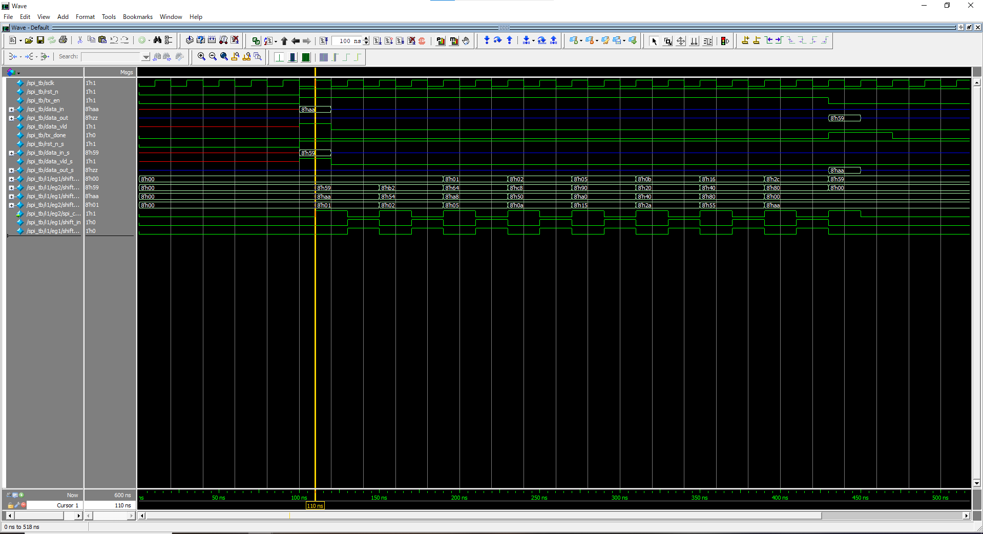
Figure 1. Verilog simulation results of SPI communication protocol (0-450ns) (Photo/Picture credit: Original).
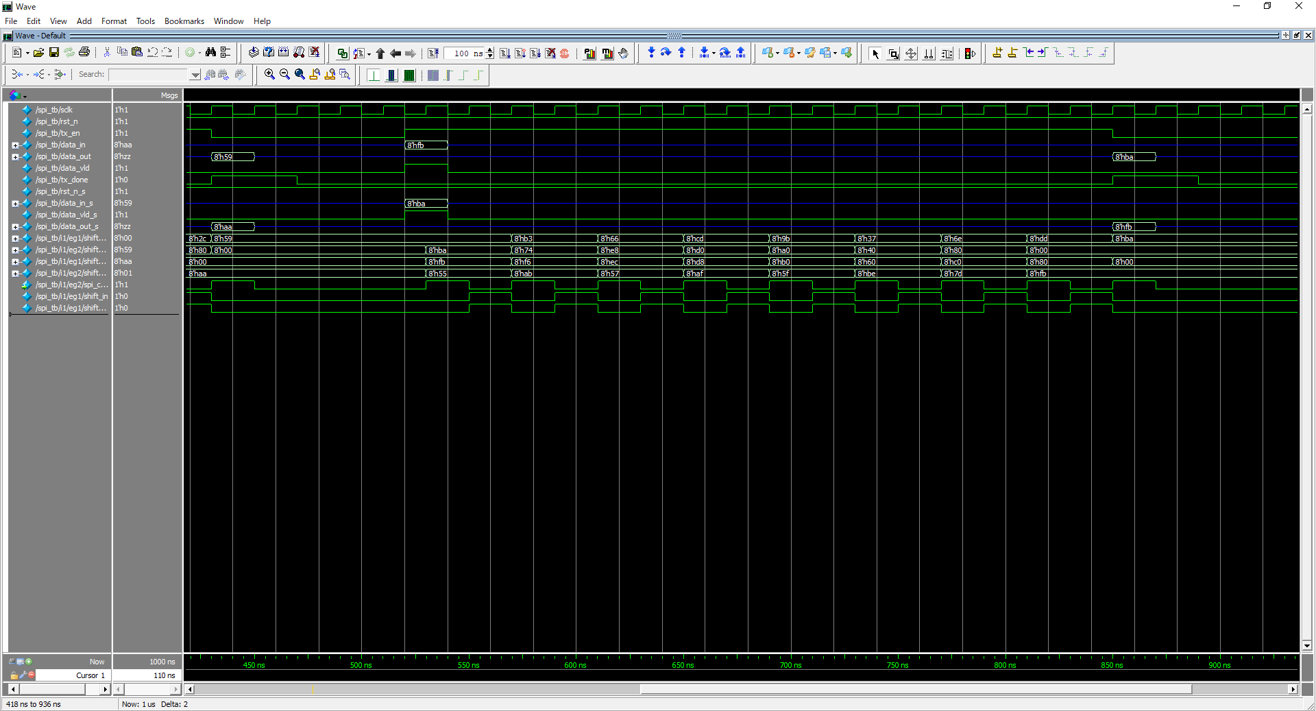
Figure 2. Verilog simulation results of SPI communication protocol (450-870ns) (Photo/Picture credit: Original).
Take the sending direction of the host as an example. In this simulation, the external input 8-bit signal data_in is synchronized with the data_vld. When the data_vld is at high power level and the sclk rising edge arrives, the external data 8 'haa is written into the internal 8-bit register shift_in_reg of the host. After every two sclk cycles, when the sclk rising edge arrives, shift_in_reg shifts 1 bit to the left, to 8 'h54, and the highest bit is transmitted to the slave via the SPI_mosi line. When the rising edge of SPI_clk comes, a 1-bit signal from SPI_mosi, 8 'h01, is received from shift_out_s, an 8-bit register inside the device, from the lowest to the highest bit. The above shift operation is performed eight times consecutively to complete the transmission of the internal register of the host device to the internal register of the slave device. shift_in_reg becomes 8 'h00, shift_out_s becomes 8' haa, the tx_done signal becomes high, and the data stored from the machine is written to data_out_s through the assign statement. You can see that the data_out_s changes to 8 'haa, indicating that the slave computer successfully receives the 8-bit data sent by the host.
5. Conclusion
The performance and stability of SPI protocol in Verilog implementation depends on many factors. The design of signal quality, including timing, noise suppression, clock jitter and other factors have a great impact on the data transmission rate and transmission stability. Whether the designed interface can adapt to different peripherals and controllers, and whether it can meet the operation requirements in different scenarios is also very important. At the same time, the overall performance and debugging of the hardware system need to be considered.
At present, serial communication protocols usually have the advantages of high transmission rate, low channel requirements, and low power consumption, so they are widely used in some fields requiring high-speed data transmission, such as intra-chip communication, embedded systems, industrial automation, and so on. However, with the continuous improvement of device complexity and data amount, the requirements for reliability, stability and efficiency of serial communication protocols are constantly increasing. In addition, with the diversification and personalization of application scenarios, the flexibility and compatibility of communication protocols are becoming more and more important.
Therefore, for the wide variety of serial communication protocols and compatibility between different devices, we can consider designing a common protocol standard to improve the efficiency and reliability of communication. At the same time, more advanced technologies, such as optical transmission and quantum communication, are considered to meet the needs of higher data transmission rates and lower fluctuations. With the continuous occurrence of various data leaks and attacks, data security and confidentiality can be incorporated into the protocol design, such as the use of encryption algorithms. With the continuous development of the contemporary Internet of Things, the demand for serial communication protocols in terms of volume and power consumption continues to increase, and more lightweight and low-energy protocol standards can be designed to meet the needs of the Internet of Things.
Authors ContributionAll the authors contributed equally and their names were listed in alphabetical order.
References
[1]. Man Liu. Design and Implementation of SPI Protocol Interface. Xidian University, 2021.
[2]. Dongliang Jia. Research and Design of All Digital Phase-locked Loop (PLL) for SoC Clock. Nanjing University of Posts and Telecommunications, 2023.
[3]. James E. Stine. Digital Computer Arithmetic Datapath Design Using Verilog HDL, 2022.
[4]. Dawei Wang. Design and Verification of SPI Interface IP Core Based on UVM. North China University of Technology, 2023.
[5]. Boxiong Jia. IC Design and Research of SPI_IP Core Based on AMBA. North University of China, 2023.
[6]. Yang Xu. Design and Verification of High-Speed SPI Interface Circuit. Xidian University, 2021.
[7]. Stuart Sutherland, Simon Davidmann, Peter Flake. SystemVerilog For Design, 2022.
[8]. Fengjun Sun, Chunxuan Yu. Verilog Implementation of SPI Serial Bus Interface. Modern electronic technology, 2005, (16):105-106+109.
[9]. Hoppe Bernhard. Verilog: Model bildung für Synthese und Verifikation. 2006.
[10]. Vaibbhav Taraate. Digital Logic Design Using Verilog, 2021.
[11]. Kung Y, Quynh V N, Hieu T N, et al. Simulink/Modelsim Co-Simulation and FPGA Realization of Speed Control IC for PMSM Drive. Intelligent Information Technology Application Association. Proceedings of the 2011 International Conference on Power Electronics and Engineering Application (PEEA 2011). Elsevier, 2011:10.
[12]. Zhigang Chen. Research and Application of VHDL Simulation Technology Based on ModelSim. Computer Knowledge and Technology, 2019, 15(31): 286-287.
[13]. Zhang qiu. Circuit Architecture Test Verification Based on Hardware Software Co-design with ModelSim. IETE Journal of Research. 2014, 59(2): 132-140.
Cite this article
Jiang,B.;Wang,S.;Zhang,S. (2024). Design and simulation implementation of SPI protocol interface based on Verilog. Applied and Computational Engineering,35,159-164.
Data availability
The datasets used and/or analyzed during the current study will be available from the authors upon reasonable request.
Disclaimer/Publisher's Note
The statements, opinions and data contained in all publications are solely those of the individual author(s) and contributor(s) and not of EWA Publishing and/or the editor(s). EWA Publishing and/or the editor(s) disclaim responsibility for any injury to people or property resulting from any ideas, methods, instructions or products referred to in the content.
About volume
Volume title: Proceedings of the 2023 International Conference on Machine Learning and Automation
© 2024 by the author(s). Licensee EWA Publishing, Oxford, UK. This article is an open access article distributed under the terms and
conditions of the Creative Commons Attribution (CC BY) license. Authors who
publish this series agree to the following terms:
1. Authors retain copyright and grant the series right of first publication with the work simultaneously licensed under a Creative Commons
Attribution License that allows others to share the work with an acknowledgment of the work's authorship and initial publication in this
series.
2. Authors are able to enter into separate, additional contractual arrangements for the non-exclusive distribution of the series's published
version of the work (e.g., post it to an institutional repository or publish it in a book), with an acknowledgment of its initial
publication in this series.
3. Authors are permitted and encouraged to post their work online (e.g., in institutional repositories or on their website) prior to and
during the submission process, as it can lead to productive exchanges, as well as earlier and greater citation of published work (See
Open access policy for details).
References
[1]. Man Liu. Design and Implementation of SPI Protocol Interface. Xidian University, 2021.
[2]. Dongliang Jia. Research and Design of All Digital Phase-locked Loop (PLL) for SoC Clock. Nanjing University of Posts and Telecommunications, 2023.
[3]. James E. Stine. Digital Computer Arithmetic Datapath Design Using Verilog HDL, 2022.
[4]. Dawei Wang. Design and Verification of SPI Interface IP Core Based on UVM. North China University of Technology, 2023.
[5]. Boxiong Jia. IC Design and Research of SPI_IP Core Based on AMBA. North University of China, 2023.
[6]. Yang Xu. Design and Verification of High-Speed SPI Interface Circuit. Xidian University, 2021.
[7]. Stuart Sutherland, Simon Davidmann, Peter Flake. SystemVerilog For Design, 2022.
[8]. Fengjun Sun, Chunxuan Yu. Verilog Implementation of SPI Serial Bus Interface. Modern electronic technology, 2005, (16):105-106+109.
[9]. Hoppe Bernhard. Verilog: Model bildung für Synthese und Verifikation. 2006.
[10]. Vaibbhav Taraate. Digital Logic Design Using Verilog, 2021.
[11]. Kung Y, Quynh V N, Hieu T N, et al. Simulink/Modelsim Co-Simulation and FPGA Realization of Speed Control IC for PMSM Drive. Intelligent Information Technology Application Association. Proceedings of the 2011 International Conference on Power Electronics and Engineering Application (PEEA 2011). Elsevier, 2011:10.
[12]. Zhigang Chen. Research and Application of VHDL Simulation Technology Based on ModelSim. Computer Knowledge and Technology, 2019, 15(31): 286-287.
[13]. Zhang qiu. Circuit Architecture Test Verification Based on Hardware Software Co-design with ModelSim. IETE Journal of Research. 2014, 59(2): 132-140.