


1. Introduction
The evolution and intricacies of electronics predominantly oscillate between analog and digital circuits, each with its unique attributes, yet interwoven in foundational principles and applications. This duality underscores many of today’s technological advancements.
Additionally, tools like Multisim, a simulation tool based on Windows launched by the American National Instruments Company, play a pivotal role in the design and simulation of both analog and digital circuits. Such tools, with their rich component libraries and intuitive interfaces, provide practical insights into the real-world applications of circuit designs [1].
Analog circuits, traditionally the backbone of electronic systems, are engineered to process signals continuous in both time and amplitude. Such circuits produce outputs often exhibiting a linear relationship with their inputs. Devices like transistors, field-effect transistors, and linear integrated circuits play central roles within these circuits. Based on operational frequencies, analog circuits manifest in diverse forms, from direct current to broadband circuits.
On the other hand, digital circuits, tailored for newer challenges, handle logic-level signals, executing arithmetic and logical operations on digital values. These circuits find a broad classification into combinational and sequential logic varieties. Intriguingly, even with contrasting signal processing methodologies, the genesis of digital circuits is intertwined with analog systems. Both share foundational principles of current and voltage, yet diverge in how these values persist over a cycle.
Contrary to what might be anticipated with the rise of digital systems, analog circuits remain indispensable. The intrinsically analog nature of the physical world necessitates that digital devices often integrate analog interfaces for optimal performance. A case in point is digital radios, which invariably incorporate an analog preamplifier essential for the initial phase of signal reception.
The design intricacies associated with analog circuits often surpass those of their digital counterparts. They demand a profound expertise, combined with a greater degree of manual intervention and less automation. Such complexities might account for the more prevalent shift towards digital systems in contemporary applications.
Central to the discourse on analog systems stands the amplifier, a fundamental component. Amplifiers, through a mosaic of electronic elements, bolster the voltage or current of input signals. Alongside amplifiers, advancements in functional electrical stimulators (FES) have been noteworthy. Recent designs, such as the voltage-controlled bi-phasic sinusoidal FES, offer advantages in avoiding charge accumulation over time, ensuring safer and more efficient stimulation in biomedical contexts [2]. Furthermore, the exploration of multi-band programmable gain, especially in Raman amplifiers, has shown potential in achieving user-defined target gain profiles, leveraging machine learning frameworks for pump power settings [3]. These innovations underscore the evolving landscape of analog systems, particularly in bioelectronic applications. The performance of an amplifier gets typically gauged by its ‘gain’, reflecting the amplification of an input signal. Beyond mere amplification, amplifiers enhance the signal-to-noise ratio, ensuring subsequent processing stages receive clearer and more discernible signals.
In line with this, recent advancements in CMOS technology have paved the way for the development of voltage-controlled programmable-gain amplifiers. Liu et al. introduced a design in 65-nm CMOS technology, emphasizing the adaptability and precision of such amplifiers in modern electronic systems [4].
Recognizing the interconnected nature of analog and digital circuits, and the paramount role of amplifiers in the former, this research focuses on this intersection. The design aspires to craft an amplifier anchored in foundational component designs. This amplifier not only aims to provide a preset amplification ratio but also introduces a rudimentary automatic gain control (AGC) feature. Such a venture seeks to bridge the principles of both circuit types, aiming for a confluence that capitalizes on the strengths of each.
2. Hybrid Amplifier Design: Integrating Analog and Digital Circuitry
The circuit design, based on the schematic and design blueprint, can be divided into three distinct sections:
2.1. Differential Signal Circuit
The heart of many amplification systems is the transformation of signal types, specifically from single-ended inputs to differential outputs. This kind of transformation provides several advantages, such as noise reduction and the potential for increased dynamic range.
In the design at hand, the LM353, a notable component in the domain of operational amplifiers, plays a pivotal role. Its inherent architecture is exploited to ensure that a single-ended input is seamlessly converted. Additionally, research has indicated the unique design and applications of Programmable Gain Amplifiers (PGAs) in certain scenarios, such as in Bluetooth Low Energy (BLE) systems [5]. Here’s a deeper dive into its functionality:
The first operational amplifier in the system serves as a ‘follower’. In technical terms, this is often referred to as a ‘voltage follower’ or ‘unity gain amplifier’. Its primary function is to offer a high input impedance and low output impedance. By doing so, it doesn’t amplify the signal but replicates the input voltage to its output, providing a buffered version of the input, which ensures that the subsequent components in the chain are not loaded and the integrity of the signal is maintained.
Conversely, the second operational amplifier acts as an ‘inverted proportion amplifier’. This component takes on a contrasting yet complementary role. Instead of merely replicating the signal, it inverts and amplifies it based on its designed proportionality. The inversion is particularly crucial for generating a differential signal, which is essentially two complementary signals. When these two signals are subtracted from one another, the result is a signal that is twice the amplitude of the original, thereby achieving amplification.
The synergy between these two operational amplifiers, working in tandem within the differential signal circuit, ensures that the single-ended input not only gets converted but also benefits from the noise immunity and enhanced dynamic range that differential signals characteristically offer. An interesting application of the convergence of analog and digital circuits can be seen in the design of festival-colored lights controllers. These lights, commonly encountered in daily life, can be designed using a combination of analog and digital circuits to achieve diverse variations [1]. This foundational step, shown in Figure 1, sets the stage for the subsequent phases of the amplification process, ensuring that the rest of the system operates with an optimized, high-quality differential signal.
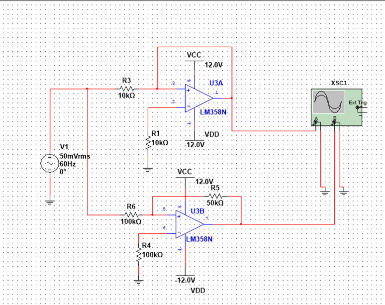
Figure 1. Differential Signal Circuit.
2.2. Amplification Circuit Design
Achieving precision in amplification, especially when multiple ratios are a prerequisite, demands rigorous design considerations. With an objective to achieve eight distinct amplification ratios, the journey began with a critical decision-making process: selecting the optimal amplification configuration.
Beyond traditional configurations, there’s a growing interest in the domain of IoT sensors where CMOS low noise amplifiers tailored for millimeter-wave applications are gaining traction. Such designs, as highlighted by Bhuiyan et al. [6], are pivotal in ensuring optimal performance and adaptability in modern electronic systems.
Modern electronics offers a plethora of choices when it comes to operational amplifiers. However, to ensure superior signal quality and minimal interference, the design’s primary concern was the common-mode rejection ratio (CMRR). A high CMRR is indicative of an amplifier’s ability to reject any signals that are common to both input terminals, which in turn greatly enhances the clarity and purity of the amplified signal.
Recent studies have delved into the intricacies of CMOS op-amp designs, highlighting the benefits of indirect feedback compensation for enhanced amplifier performance and stability [7]. Furthermore, the realm of amplifier designs has seen innovations in multi-band programmable gain, especially in Raman amplifiers, which utilize machine learning frameworks for optimal pump power settings [8]. Such advancements underscore the significance of adaptability and precision in modern amplifier designs, as further demonstrated by AbuShawish’s work on tunable UGBW rail-to-rail CMOS op-amps in bio-medical signal detection systems [9].
In the exploration phase, two configurations were juxtaposed: a single operational amplifier system versus a more intricate setup involving three operational amplifiers. It was evident from theoretical evaluations and preliminary tests that the trio configuration outclassed its single counterpart in terms of CMRR. The tri-amplifier design not only brought the advantage of a higher CMRR but also allowed for more flexibility and finetuning, especially when targeting multiple amplification ratios.
Another salient criterion was the need for a large input impedance referring to Figure 2. This is essential to ensure that the amplification circuit doesn’t unduly load or distort the signal source, preserving the integrity of the input signal. The tri-amplifier configuration inherently offers a higher input impedance, making it a more fitting choice for applications requiring minimal influence on the connected source.
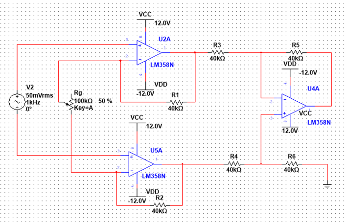
Figure 2. Amplification Circuit Design.
Following the establishment of the foundational design, meticulous simulations and mathematical models were employed to determine precise resistor values for achieving the targeted amplification ratios. These ratios spanned from moderate values like -2 times to more extensive amplifications such as -50 times. The simulations played a vital role in ensuring theoretical expectations matched real-world outcomes. Each resistor value was derived through a blend of empirical testing and theoretical calculations, creating a balance between design foresight and experimental validations. Achieving precision in amplification, especially when multiple ratios are a prerequisite, demands rigorous design considerations. Modern electronics offers a plethora of choices when it comes to operational amplifiers. However, to ensure superior signal quality and minimal interference, the design’s primary concern was the common-mode rejection ratio (CMRR). A high CMRR is indicative of an amplifier’s ability to reject any signals that are common to both input terminals, which in turn greatly enhances the clarity and purity of the amplified signal [10]. The comprehensive calculations, which serve as a testament to the rigor and precision of the design process, are detailed subsequently. Simulations and calculations have determined the resistor values corresponding to amplification ratios of -2, -5, -10, -15, -20, -30, -40, and -50 times. The detailed calculations are as follows:
From the theoretical calculation results, we conclude that: when \( {R_{1}}={R_{2}}, {R_{3}}={R_{4}} \) , \( {R_{5}}={R_{6}} \) ,
\( {A_{uf}}=\frac{{U_{O}}}{{U_{i1}}-{U_{i2}}} \) =- \( \frac{{R_{5}}}{{R_{3}}} \) (1+ \( \frac{{2R_{1}}}{{R_{g}}} \) ) (1)
For ease of calculation, we make the \( {R_{1}}={R_{2}}={R_{3}}={R_{4}}{=R_{5}}={R_{6}}=R=40KΩ \) , \( {A_{uf}}=\frac{{U_{O}}}{{U_{i1}}-{U_{i2}}} \) =- \( \frac{{R_{5}}}{{R_{3}}} \) (1+ \( \frac{{2R_{1}}}{{R_{g}}} \) )= 1+ \( \frac{2R}{{R_{g}}} \) .
The load resistance value required by different magnifications can be obtained as shown in Table 1:
Table 1. Characteristics of the Amplifier: Address, Auf, and Rg(KΩ).
Address | Auf | Rg(KΩ) |
000 | -2 | 80 |
001 | -5 | 20 |
010 | -10 | 8.88 |
011 | -15 | 5.7 |
100 | -20 | 4.2 |
101 | -30 | 2.75 |
110 | -40 | 2.05 |
111 | -50 | 1.63 |
2.3. Load Conversion Circuit
The CD4051/CC4051 represents a single 8-channel digitally controlled analog switch, as shown in Figure 3. It features three binary control input terminals, A, B, C, along with an INH input and is characterized by its low on-resistance and minimal cutoff leakage current. Digital signals with an amplitude ranging from 4.5 to 20V can control analog signals with peak values up to 20V. For instance, if VDD = +5V, VSS = 0, and VEE = -13.5V, then a digital signal ranging from 0 to 5V can control an analog signal ranging from -13.5V to 4.5V. These switch circuits maintain an extremely low static power consumption across the entire VDD-VSS and VDD-VEE power range, regardless of the logic state of the control signal. All channels are cut off when the INH input equals “1”. A three-bit binary signal selects one of the eight channels, connecting that input to the output.
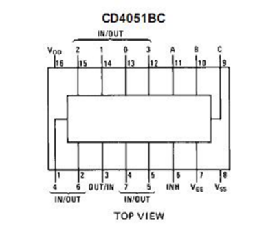
Figure 3. The tube pin diagram of CD4051.
Based on theoretical computations, appropriate voltages and potentiometers are chosen to achieve the designated amplification ratios. Leveraging the channel selection mode of the CD4051 chip, inputs ranging from 000 to 111 are fed into the ABC terminals, facilitating the channel’s conductivity, thereby allowing for the alteration of amplification ratios.
This section represents the sole digital circuit component in the entire design process, illustrated in Figure 4.
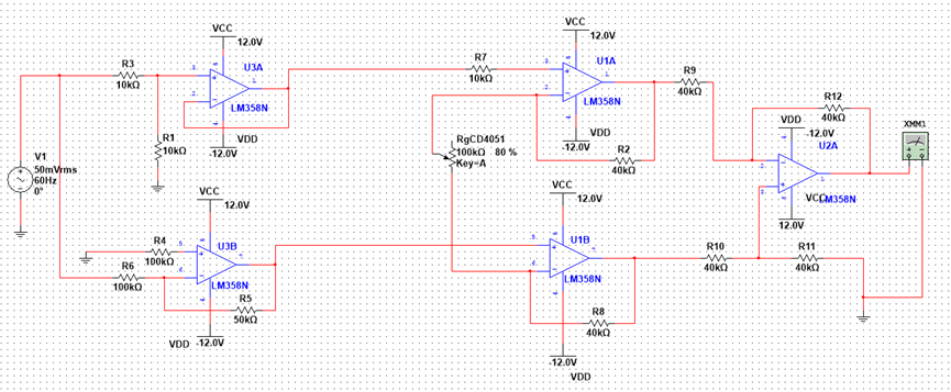
Figure 4. Complete circuit design diagram.
2.4. Experimental Conclusion
After meticulously building the circuit, as illustrated in Figure 5, in the laboratory using the actual components as outlined in the design blueprint, rigorous testing was carried out to evaluate its performance and operational capabilities.
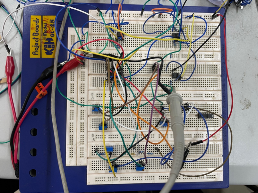
Figure 5. A circuit built in the laboratory.
The design’s primary objective was to amplify an input signal by predetermined ratios. Post-construction, the circuit was subjected to various inputs, with the intent to analyze its amplification performance. Gratifyingly, it was observed that the circuit proficiently amplified the input signals by the predefined ratios. The amplification levels attained during the tests were consistent with the theoretical calculations, demonstrating the reliability and accuracy of the design.
The input signal is set to be 50 mV sine signal, and the results of the output signal are presented in Table 2.
Table 2. Comparison of Amplifier Output: Av, Actual vs. Theoretical Signals, and Fractional Error.
Av | Actual output signal | Theoretical output signal | fractional error |
-2 | 97mV | 100mV | 3% |
-5 | 248mV | 250mV | 0.8% |
-10 | 500mV | 500mV | 0% |
-15 | 753mV | 750mV | 0.4% |
-20 | 0.99V | 1V | 1% |
-30 | 1.51V | 1.5V | 0.6% |
-40 | 1.96V | 2V | 2% |
-50 | 2.48V | 2.5V | 0.8% |
Furthermore, the use of components, particularly the LM353 for the differential signal circuit and the CD4051 for the load conversion circuit, showcased their effectiveness in achieving the desired amplification ratios. The results solidly echo the theoretical underpinnings, as the differential signal circuit effectively transformed single-ended input signals into differential outputs, while the amplification circuit ensured the attainment of the eight stipulated amplification ratios.
One noteworthy observation was the fidelity with which the amplification ratios were achieved. There were minimal deviations, further asserting the precision of the design. Moreover, the incorporation of the load conversion circuit successfully allowed for the modulation of amplification ratios based on the input provided to the ABC terminals of the CD4051 chip.
In conclusion, the design successfully meets its intended purpose of amplifying input signals by predetermined ratios. The empirical evidence gathered from the laboratory testing corroborates the design’s credibility and reliability. It is a testament to the robustness of the theoretical framework, careful component selection, and meticulous construction. The set of successful amplification signals is depicted in Figure 6.
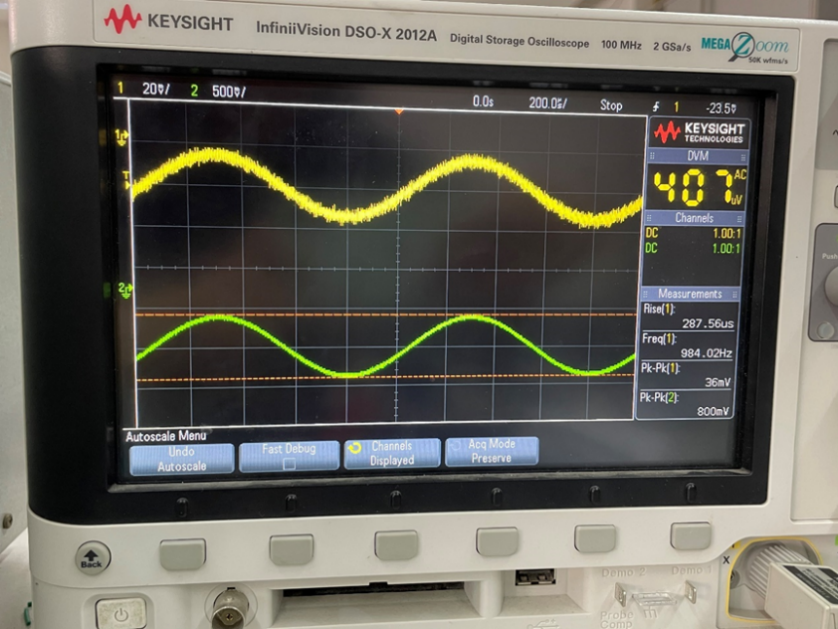
Figure 6. A set of successful amplification signals.
2.5. Problems and solutions
2.5.1. Signal Transmission Issues
Upon assembling the amplification circuit according to the schematic, it was found that an oscilloscope could not detect any waveform. By employing a multimeter for systematic troubleshooting, a discrepancy between the voltage at the LM324 pin and the simulation results was detected. To address this, the LM324 was replaced with two LM353 chips. This not only streamlined the circuit structure but also successfully displayed the waveform on the oscilloscope.
2.5.2. Waveform Distortion
With proper outputs from both the NE555 and 74LS161, an error in the waveform, shown in Figure 7, output from the 74LS138 was identified. After ensuring that the wiring was correct and inspecting each pin individually, it was discovered that one of the pins was outputting an incorrect voltage. The problem was resolved by replacing the chip, after which the 74LS138 produced the expected square wave output.
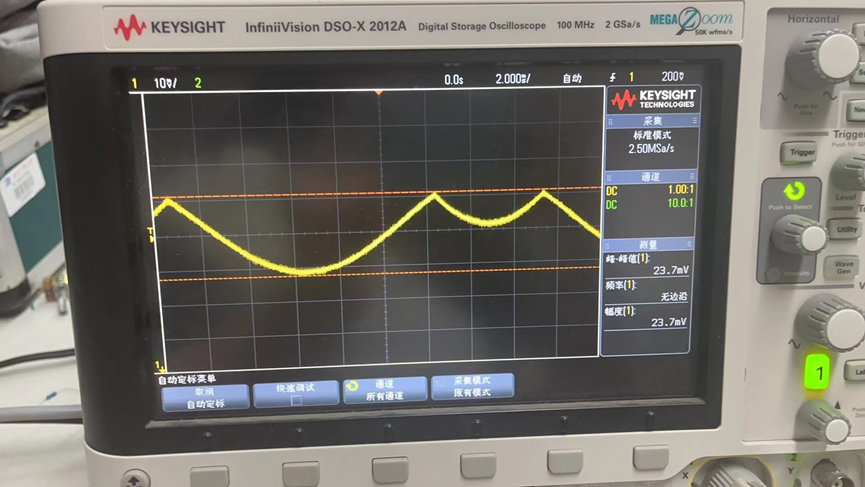
Figure 7. An error in the waveform.
2.5.3. Address Channel Mismatch
When altering addresses to inspect waveform amplification ratios with an oscilloscope, the observed ratios did not align with theoretical expectations. The amplification ratios corresponding to channel addresses were inconsistent with the calculations. On closer inspection of the address channels and potentiometer values, a wiring error was identified where the sequence of A, B, and C inputs was inadvertently inverted. This reversal led to a mismatch in the amplification ratios for different channels. After correctly wiring the A, B, and C sequences, the amplification ratios for distinct addresses finally matched the theoretical values.
3. Conclusions
Drawing from both in-depth theoretical analysis of circuit design and the conclusive findings from experimental verification, it is established that the amplifier can consistently and accurately amplify input signals in accordance with the predetermined amplification ratios. Employing a spectrum of basic electronic components, this design embodies a novel convergence of digital and analog circuitry. Such a synthesis not only contributes to the creation of an amplifier of tangible utility but also suggests its potential applicability in more sophisticated circuits where signal modulation and management become paramount.
Moreover, the ability of this amplifier to serve as an intermediate device in complex circuits accentuates its potential in enhancing the efficiency and efficacy of signal processing. It, thus, can act as a bridge ensuring that the subsequent stages of signal processing are more efficient and error-free.
However, every innovation, while it offers novel solutions, also brings along its set of challenges. One of the more pronounced limitations of this design is its susceptibility to external interferences. The current model’s defense mechanism against potential disruptions, particularly from unpredictable external sources, is an area that requires attention and fortification. Enhancing its robustness against such anomalies can drastically increase its reliability and broaden its application spectrum.
Furthermore, for the amplifier to be universally adaptable and cater to a diverse range of operational requirements, it is essential to undertake iterative design modifications. This would ensure its compatibility with different scenarios and extend its utility across varied applications. It’s worth noting that while the foundational design has showcased promise, its evolution through subsequent refinements will determine its long-term relevance and applicability.
References
[1]. Zhang H, He C & Wang W. 2021 Application of Multisim in Analog Circuit and Digital Circuit Courses (Electronic Production vol 04) (Beijing: Electronic Production Press) pp 17–19.
[2]. Júnior, Isaías & Freire, Raimundo & Venuto, Edelson. (2020). Design of a Programmable Gain Amplifier (PGA) for Bluetooth Low Energy (BLE) in 0.13 um CMOS. Journal of Integrated Circuits and Systems. 15. 1-9.
[3]. Bai, Chunfeng & Wu, Jianhui & Deng, Xiaoying. (2018). A Review of CMOS Variable Gain Amplifiers and Programmable Gain Amplifiers. IETE Technical Review. 36. 1-17.
[4]. Szytula A and Leciejewicz J 1989 HandbKumar, Kandi & Vaithiyanathan, D. (2020). Design and analysis of a three stage CMOS op-amp using indirect feedback compensation. Journal of Physics: Conference Series. 1706. 012055.
[5]. De Moura, U. C., Iqbal, M. A., Kamalian, M., Krzczanowicz, L., Da Ros, F., Brusin, A. M. R., … Zibar, D. (2021). Multi–Band Programmable Gain Raman Amplifier. Journal of Lightwave Technology, 39(2), 429–438.
[6]. AbuShawish, I. Y., & Mahmoud, S. A. (2021). A programmable gain and bandwidth amplifier based on tunable UGBW rail-to-rail CMOS op-amps suitable for different bio-medical signal detection systems. AEU - International Journal of Electronics and Communications, 141, 153952.
[7]. Liu, Hang; Zhu, Xi; Lu, Muting; Yeo, Kiat Seng (2019). [IEEE 2019 IEEE/MTT-S International Microwave Symposium - IMS 2019 - Boston, MA, USA (2019.6.2-2019.6.7)] 2019 IEEE MTT-S International Microwave Symposium (IMS) - Design of a Voltage-Controlled Programmable-Gain Amplifier in 65-nm CMOS Technology. 87–90.
[8]. Leung, Fu-Shing; Liu, Don-Gey; Lai, Weidian; Shiau, Miin-Shyue; Wu, Hong-Chong; Zheng, Ziwei (2019). [IEEE 2019 8th International Symposium on Next Generation Electronics (ISNE) - Zhengzhou, China (2019.10.9-2019.10.10)] 2019 8th International Symposium on Next Generation Electronics (ISNE) - Design of a Programmable Biomedical Front-End Amplifier with Pseudo Resistors. 1–3.
[9]. Chen, Wei-Hsien; Chang, Chia-Hung; Shih, Horng-Yuan; Chiu, Tzai-Wen; Kuo, Chien-Nan (2019). A charge accumulation-free voltage-controlled functional electrical stimulator with bi-phasic sinusoidal stimulation. Analog Integrated Circuits and Signal Processing.
[10]. Leung, Fu-Shing; Liu, Don-Gey; Lai, Weidian; Shiau, Miin-Shyue; Wu, Hong-Chong; Zheng, Ziwei (2019). [IEEE 2019 8th International Symposium on Next Generation Electronics (ISNE) - Zhengzhou, China (2019.10.9-2019.10.10)] 2019 8th International Symposium on Next Generation Electronics (ISNE) - Design of a Programmable Biomedical Front-End Amplifier with Pseudo Resistors. , (), 1–3. doi:10.1109/ISNE.2019.8896529.
Cite this article
Zhao,S. (2024). Design and implementation of a preset operational amplifier based on basic digital and analog hybrid circuit. Applied and Computational Engineering,38,112-120.
Data availability
The datasets used and/or analyzed during the current study will be available from the authors upon reasonable request.
Disclaimer/Publisher's Note
The statements, opinions and data contained in all publications are solely those of the individual author(s) and contributor(s) and not of EWA Publishing and/or the editor(s). EWA Publishing and/or the editor(s) disclaim responsibility for any injury to people or property resulting from any ideas, methods, instructions or products referred to in the content.
About volume
Volume title: Proceedings of the 2023 International Conference on Machine Learning and Automation
© 2024 by the author(s). Licensee EWA Publishing, Oxford, UK. This article is an open access article distributed under the terms and
conditions of the Creative Commons Attribution (CC BY) license. Authors who
publish this series agree to the following terms:
1. Authors retain copyright and grant the series right of first publication with the work simultaneously licensed under a Creative Commons
Attribution License that allows others to share the work with an acknowledgment of the work's authorship and initial publication in this
series.
2. Authors are able to enter into separate, additional contractual arrangements for the non-exclusive distribution of the series's published
version of the work (e.g., post it to an institutional repository or publish it in a book), with an acknowledgment of its initial
publication in this series.
3. Authors are permitted and encouraged to post their work online (e.g., in institutional repositories or on their website) prior to and
during the submission process, as it can lead to productive exchanges, as well as earlier and greater citation of published work (See
Open access policy for details).
References
[1]. Zhang H, He C & Wang W. 2021 Application of Multisim in Analog Circuit and Digital Circuit Courses (Electronic Production vol 04) (Beijing: Electronic Production Press) pp 17–19.
[2]. Júnior, Isaías & Freire, Raimundo & Venuto, Edelson. (2020). Design of a Programmable Gain Amplifier (PGA) for Bluetooth Low Energy (BLE) in 0.13 um CMOS. Journal of Integrated Circuits and Systems. 15. 1-9.
[3]. Bai, Chunfeng & Wu, Jianhui & Deng, Xiaoying. (2018). A Review of CMOS Variable Gain Amplifiers and Programmable Gain Amplifiers. IETE Technical Review. 36. 1-17.
[4]. Szytula A and Leciejewicz J 1989 HandbKumar, Kandi & Vaithiyanathan, D. (2020). Design and analysis of a three stage CMOS op-amp using indirect feedback compensation. Journal of Physics: Conference Series. 1706. 012055.
[5]. De Moura, U. C., Iqbal, M. A., Kamalian, M., Krzczanowicz, L., Da Ros, F., Brusin, A. M. R., … Zibar, D. (2021). Multi–Band Programmable Gain Raman Amplifier. Journal of Lightwave Technology, 39(2), 429–438.
[6]. AbuShawish, I. Y., & Mahmoud, S. A. (2021). A programmable gain and bandwidth amplifier based on tunable UGBW rail-to-rail CMOS op-amps suitable for different bio-medical signal detection systems. AEU - International Journal of Electronics and Communications, 141, 153952.
[7]. Liu, Hang; Zhu, Xi; Lu, Muting; Yeo, Kiat Seng (2019). [IEEE 2019 IEEE/MTT-S International Microwave Symposium - IMS 2019 - Boston, MA, USA (2019.6.2-2019.6.7)] 2019 IEEE MTT-S International Microwave Symposium (IMS) - Design of a Voltage-Controlled Programmable-Gain Amplifier in 65-nm CMOS Technology. 87–90.
[8]. Leung, Fu-Shing; Liu, Don-Gey; Lai, Weidian; Shiau, Miin-Shyue; Wu, Hong-Chong; Zheng, Ziwei (2019). [IEEE 2019 8th International Symposium on Next Generation Electronics (ISNE) - Zhengzhou, China (2019.10.9-2019.10.10)] 2019 8th International Symposium on Next Generation Electronics (ISNE) - Design of a Programmable Biomedical Front-End Amplifier with Pseudo Resistors. 1–3.
[9]. Chen, Wei-Hsien; Chang, Chia-Hung; Shih, Horng-Yuan; Chiu, Tzai-Wen; Kuo, Chien-Nan (2019). A charge accumulation-free voltage-controlled functional electrical stimulator with bi-phasic sinusoidal stimulation. Analog Integrated Circuits and Signal Processing.
[10]. Leung, Fu-Shing; Liu, Don-Gey; Lai, Weidian; Shiau, Miin-Shyue; Wu, Hong-Chong; Zheng, Ziwei (2019). [IEEE 2019 8th International Symposium on Next Generation Electronics (ISNE) - Zhengzhou, China (2019.10.9-2019.10.10)] 2019 8th International Symposium on Next Generation Electronics (ISNE) - Design of a Programmable Biomedical Front-End Amplifier with Pseudo Resistors. , (), 1–3. doi:10.1109/ISNE.2019.8896529.