


1. Introduction
In industry, Moore’s Law has a vital stage: every 18 to 24 months, when the price remains the same, while the number of transistors on the chip doubles, the performance will also double the increasing integration of the chip, the delay, power consumption and area are always the three most critical factors in determining the circuit performance [1]. A 4-bit Absolute-Value Detector is a digital circuit, which realizes the function that when given a 4-bit input number in 2’s complement format, the circuit should be able to generate its absolute value, then compare it to a specified threshold value, and finally provide a Boolean value in which 1 represents the input is greater than the threshold value and 0 for the opposite [2].
It has significant and vast applications in the industry [3]. In terms of signal processing and measurement, it can quickly and accurately measure the input signal, especially in audio, video, sensor signal processing and other fields. In terms of alarm and fault detection, it can be used to detect whether the signal is beyond the preset threshold range to ensure the normal operation and security of the signal. In the control field, it can be used to implement the PID algorithm to provide stable and accurate comparative results by comparing the size differences between the input signal and the preset target values [4]. In fact, its applications are more than the examples above. The working logic of 4-bit absolute detector is shown in figure 1.
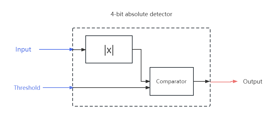
Figure 1. Working logic of 4-bit absolute detector (Photo/Picture credit: Original).
As is shown, there are two main components to the absolute-value detection. The first part is the absolute value circuit and the other one is comparator. Compared to TTL, the power consumption of CMOS is much smaller, but the speed of CMOS is inferior to TTL in most cases [5]. As a result, when this paper designs a circuit based on CMOS, delay is relatively more important factor to influence the overall performance of circuit than this consumption. How to design a CMOS based circuit with shorter delay become the main problem in the initial stage.
2. Circuit Optimization
2.1. Boolean circuit or functional circuit
Firstly, to achieve the absolute value circuit, there are two options. A functional circuit is a circuit that can be divided into functional blocks, and each functional block is interconnected and cooperates to realize the function. Boolean circuit means it is comprised of pure logic gates and the entire circuit an’t be split into smaller unit which can realize a segmented function. When this paper design a 4-bit absolute value circuit, on one hand, as a functional circuit, the basic logic is that if the input value is negative, which means A [3] is equal to 1, flip A [2:0] and add 1 to it to get the absolute value of the negative value, and that if the input value is positive, the absolute value is equal to A [2:0]. Then the absolute value circuit can be split into a selector, 3 inverters and 3-bit adder. On the other hand, as a Boolean circuit, all that needs to be done is to list the truth table, then simplify it with Karnaugh map and draw down the circuit with AND-OR gate. Finally, the absolute value circuit can be implemented through the 4-stage AND-OR gate circuit.
If draw critical path, it can be found the function one is much longer than the Boolean one. This is because in the process of implementation through the adder, because a number is fixed, a large number of doors is redundant, can be optimized, but in the process of implementation by pure logic circuit, in the case of results, each door will not overlap, each branch points to the unique result. Therefore, in this case, it is more recommended to use the pure logic circuit to achieve the absolute value circuit. So, the design of absolute value circuit is shown as figure 2 below.
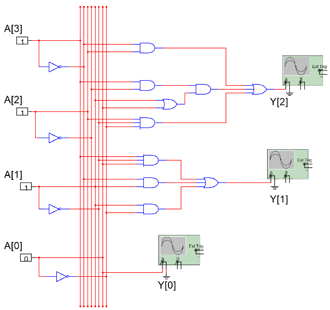
Figure 2. The circuit of absolute value (Photo/Picture credit: Original).
In the comparator circuit, there are 6 input signals. If the pure logic circuit is used, due to the input signal is more, the circuit series is more and more difficult to simplify. However, when the functional circuit is used, the three-bit comparator is divided into three one-bit comparators. If the upper level is equal, the next level is compared until the size is compared. As seen in the figure 3, each small unit has a simple structure and a clear function. Z represents the result of comparison, while carry represents whether the next 1-bit comparator works. If Y>T, Z=1. If not, Z=0. If Y=T, carry=1. If not, carry=0. In this case, it is more recommended to implement the comparator with functional circuits.
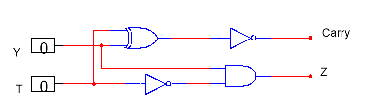
Figure 3. The circuit of 1-bit comparator (Photo/Picture credit: Original).
Therefore, it is not difficult to get this conclusion that when designing a circuit, specific analysis should be done, finally to simplify the circuit and make the logic gate less. If the number of input signals is small (less than 4) and the outputs are clear, pure logic circuit should be preferred, which is shown in figure 4.
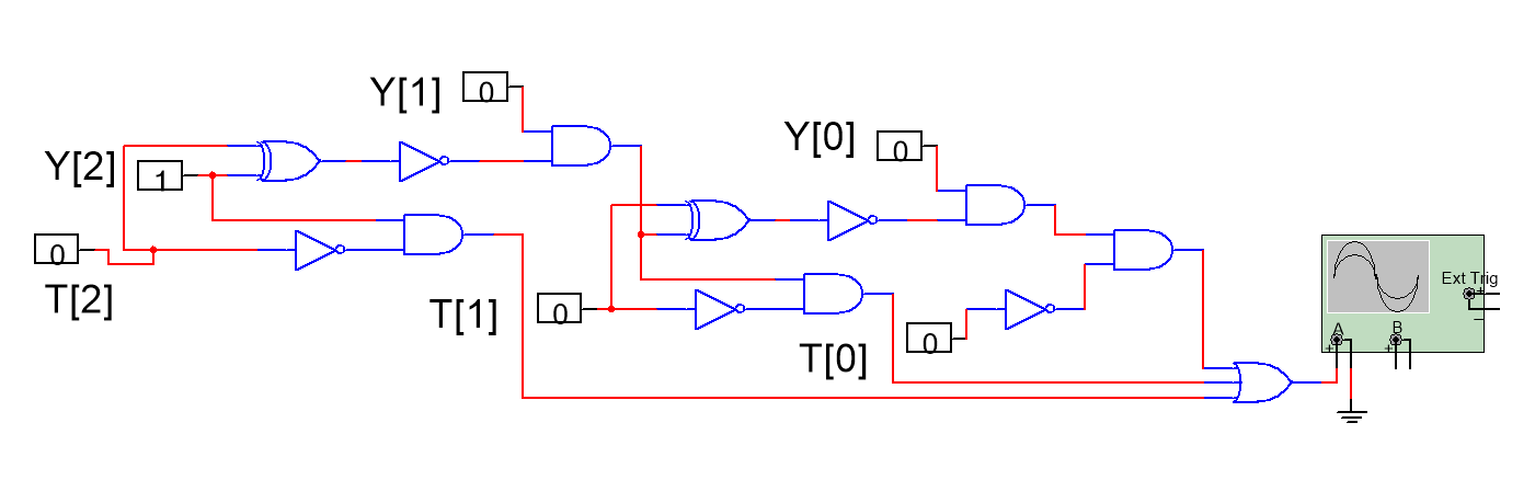
Figure 4. The circuit of 3-bit comparator (Photo/Picture credit: Original).
If there are many input signals and the overall circuit can be split into simple and repeated unit, functional circuit may be better.
2.2. The priority of the logic gate
Commonly used logic gates are AND gate, OR gate, NOT gate, XOR gate. If Complementary Static CMOS is used, as shown in the figure 5 below, this paper can see the transistor structure of each logic gate.
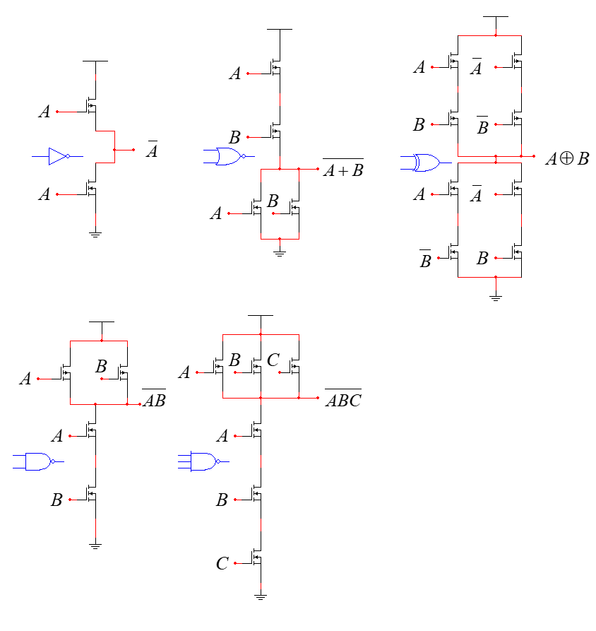
Figure 5. The circuit of logic gates (Photo/Picture credit: Original).
2.2.1. The model of delay
From the basic concept of RC, this paper can get
\( Delay=RgateCload+RgateCself \) (1)
Then this paper assumes 3 variables  .
.  is the normalized delay.
  is known as the effort delay.
  is the known as the parasitic delay [6]. So, this paper can get
\( d=f+p \) (2)
Next, this paper makes  normalized to the delay of a FO-1 inverter (no self-load). With
  ,
, fanout + normalized parasitic, so
  is essentially equivalent to fanout.
 is a variable that is independent of process, voltage, and temperature. So, this paper can get
\( d=Delay/τ=(RgateCload+RgateCself)/R0C0 \) (3)
Then this paper can list the formula of  according to the figure 5.
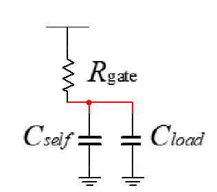
Figure 5. RC model of the delay (Photo/Picture credit: Original).
\( tp=0.69Rg(Cpar+Cout) \) \( =0.69RgCin,gate(\frac{Cpar}{Cin,gate}+\frac{Cout}{Cin,gate}) \) \( =τgate(γgate+\frac{Cout}{Cin,gate}) \) (4)
As a result, if this paper normalizes the delay to fictitious “technology time constant”, this paper can get
\( \frac{Delay}{τINV}=\frac{τgate}{τINV}(γgate+\frac{Cout}{Cin,gate}) \) (5)
Assume that
\( g=\frac{RgateCin,gate}{RINVCin,INV} \) (6)
\( h=\frac{Cout}{Cin,gate} \) (7)
\( p=\frac{Cpar,gate}{Cpar,INV} \) (8)
Finally, this paper can get
\( d=g(γgate+h)=gh+pγ=f+p \) (9)
2.2.2. Comparison of logic gate delays
From the circuit topology, it can be found that an AND gate is equivalent to a circuit a NOT gate and a NOT gate, while an OR gate is equivalent to an NOR gate and an inverter, so the priority of the NAND gate is higher than that of the AND gate, and similarly, the priority of an NOR gate is higher than that of the OR gate. An XOR gate is equivalent to two 2-input AND gate and a 2-input OR gate, and after calculation, it can be found that the XOR gate delay is more than the total delay with the AND-OR gate. Moreover, XOR can have TPL and other forms to further reduce the delay, so the XOR gate has the highest priority [7, 8].
Given  /
/ , this paper can calculate the
  of different logic gates. Through calculation, if this paper takes NOR as example and assume that n is the number of inputs, this paper can get
\( g=\frac{n\cdot {W_{P}}+{W_{N}}}{{W_{P}}+{W_{N}}} \) (10)
\( p=\frac{n\cdot {W_{P}}+n\cdot {W_{N}}}{{W_{P}}+{W_{N}}}=n \) (11)
Assume that  , according to
  , this paper can get the figure 6 as below.
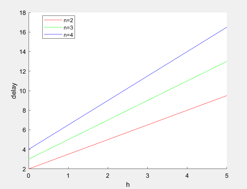
Figure 6. The curve of the delay of NOR gate with different number of inputs (Photo/Picture credit: Original).
As the number of inputs increases, as shown in the figure above, a 3-input NOR gate can be split into a 2-input NAND gate and a 2-input NOR gate [9]. Through calculation, it can be verified that the delay of a 3-input NAND gate is greater than the total delay of a 2-input NOR gate and a 2-input NAND gate. Likewise, it can be demonstrated that the priority of the n-input gates is higher than that of (n-1)-input gates. Finally, this paper can get such a priority relationship as shown in table 1.
Table 1. The priority of logic gates.
1 | 2 | 3 | 4 | 5 | … |
XOR | n-input NAND/NOR | n-input AND/OR | n-1-input NAND/NOR | n-1-input AND/OR | … |
As a result, this paper can optimize the circuit as figure 7 below.
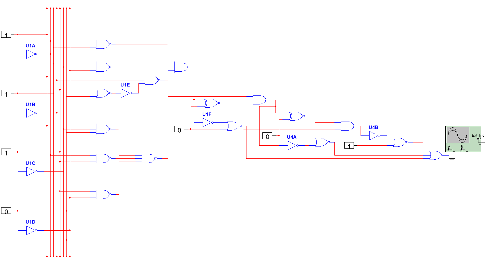
Figure 7. The optimized circuit with higher priority (Photo/Picture credit: Original).
2.3. the number of stages of critical path
2.3.1. Calculate the optimum number of stages of critical path
The Inverter chain is shown in figure 8 [10].
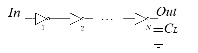
Figure 8. Inverter chain [10].
From the figure above, this paper can get
\( tp=tp1+tp2+…+tpN \) (12)
Because
\( tpj~Rgate,unitCin,gate,unit(γ+\frac{Cgin,j+1}{Cgin,j}) \) (13)
So
\( tp=\sum _{j=1}^{N}tp,j=τ\sum _{i=1}^{N}(γ+\frac{Cgin,j+1}{Cgin,j}),Cgin,N+1=CL \) (14)
As you can see, the equation has N-1 unknowns. So, this paper performs partial derivatives on these N-1 unknowns to find the minimum value of the delay. Finally, this paper gets the conclusion that when the delay is minimal, it satisfies the condition that
\( \frac{Cgin,j+1}{Cgin,j}=\frac{Cgin,j}{Cgin,j-1} \) (15)
So when
\( Cgin,j=\sqrt[]{Cgin,j-1\cdot Cgin,j+1} \) (16)
it has the minimum delay and each stage has the same fanout and delay.
When each stage is sized by  and has the same fanout
  :
:
\( {f^{N}}=F=\frac{CL}{Cgin,1} \) (17)
\( f=\sqrt[N]{F} \) (18)
\( tp=Nτ(γ+\sqrt[N]{F}) \) (19)
So, the optimal number of stages can get
\( {C_{L}}=F\cdot {C_{in}}={f^{N}}{C_{in}}⇒N=\frac{ln{F}}{ln{f}} \) \( ⇒{t_{p}}=Nτ({F^{1/N}}+γ)=\frac{{t_{p0}}ln{F}}{γ}(\frac{f}{ln{f}}+\frac{γ}{ln{f}}) \) \( ⇒\frac{δ{t_{p}}}{δf}=\frac{{t_{p0}}ln{F}}{γ}\cdot \frac{ln{f}-1-γ/f}{{ln^{2}}{f}}=0 \) \( ⇒f=exp{(}1+γ/f) \) (20)
For 

\( N=ln{F} \) (21)
So this paper assume that  ,
,  , this paper can get the optimal number is 3.47, which means if the number of stages of critical path is 3 or 4, it may have the smallest delay.
2.3.2. Optimize circuit delay by decreasing or increasing the number of stages
According to the present circuit, this paper can find the critical path and count the number of stages.
Typically, the stages of critical path are much more than the optimal stages for a circuit to implement a relatively more complex function, so here this paper is mainly discussing about reducing the number of stages. If increasing the number of stages is needed, just do the opposite.
Here this paper proposes three kinds of solutions.
The first one is to optimize the logic. This paper can try to classify different kinds of cases of the truth table in multiple ways to avoid certain kinds of cases where the logic is too complicated. If some common submodules are needed, you can try to use encapsulated circuits, which often have been optimized to the best. The second one is to use logic gates with more inputs. It’s easy to comprehend that a logic gate with more inputs can replace two or more logic gates, such reducing the number of stages. But what needs to take notice is that that’s not always the case because the logic gates in the critical paths may have their branches so that if you use a more complicated gates with more inputs, you may cover cases in the branch thus complicating the critical path and increase the delay.
The third one is to replace series with parallel. This is a very valid solution to reduce delay. When there are many modules, consider how to connect them with each other in parallel to shorten the length of the total critical path. Finally, the optimal circuit of this paper is as below in figure 9.
Figure 9. The optimized circuit with fewer stages (Photo/Picture credit: Original).
3. Optimization of delay and power consumption based on varying sizing and
3.1. the optimization of delay
3.1.1. the calculation of the optimal sizing of logic gates in critical path
The model of a circuit with branches is shown in figure 10.
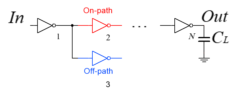
Figure 10. The model of a circuit with branches (Photo/Picture credit: Original).
Based on the theory of 2.2, considering the effect of branching on delay, this paper adds branching effort to the theory. For each logic gate with a branch, it has branching effort  ,
,
\( b=\frac{{C_{on-path}}+{C_{off-path}}}{{C_{on-path}}} \) (22)
For example, as shown in figure, inverter 1 has 2 branches, so
\( {b_{1}}=\frac{{C_{gin,2}}+{C_{gin,3}}}{{C_{gin,2}}} \) (23)
Path Branching Effort: 
Now this paper can compute the path effort
\( {F_{path}}=GBH=\prod g\cdot b\cdot h \) (24)
As a result,
\( Dela{y_{path}}=F+P=GBH+P \) (25)
Based on the concept in 2.3.1 this paper can get when ,the total delay is minimum, so
\( {f^{*}}=\sqrt[N]{F}=ghb=gb\frac{{C_{out}}}{{C_{in}}} \) (26)
Finally, this paper can determine the optimal gate sizes:
\( {C_{in}}=g\cdot b\cdot \frac{{C_{out}}}{{f^{*}}} \) (27)
3.1.2. The calculation of minimum delay
The Critical path is shown in figure 11.
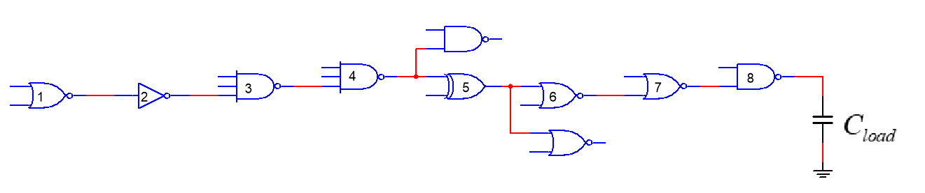
Figure 11. Critical path (Photo/Picture credit: Original).
Assume that  , through calculation, this paper can get the calculation of parameters of each stage shown in table 2.
Table 2. The calculation of parameters of each stage.
stage | 1 | 2 | 3 | 4 | 5 | 6 | 7 | 8 |
cls | NOR | INV | NAND(3i) | NAND(3i) | XOR | NOR | NOR | NAND |
b | 1 | 1 | 1 | 2.4 | 2 | 1 | 1 | 1 |
g | 1.602 | 1 | 1.796 | 1.796 | 4 | 1.602 | 1.602 | 1.398 |
p | 2 | 1 | 3 | 3 | 4 | 2 | 2 | 2 |
size’ | 2 | 3.42 | 9.38 | 14.33 | 16.22 | 5.56 | 9.53 | 16.31 |
Assume that 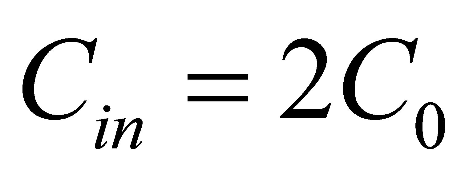 ,
, , so
, so
\( H=\prod {h_{i}}=\frac{{C_{gin,1}}}{{C_{in}}}\cdot \frac{{C_{gin,2}}}{{C_{gin,1}}}\cdot \frac{{C_{gin,3}}}{{C_{gin,2}}}⋯\frac{{C_{gin,8}}}{{C_{gin,7}}}\cdot \frac{{C_{load}}}{{C_{gin,8}}} \) =16 (28)
\( G=\prod {g_{i}}=1.6\text{^}3*1.1*1.8\text{^}3=33.44 \) (29)
\( B=\prod {b_{i}}=2*2.4=4.8 \) (30)
\( F=BGH=3203.1 \) (31)
\( {f^{*}}=\sqrt[8]{F}=2.743 \) (32)
 ns (33)
When the delay is minimized, the sizing of each gate can be obtained according to  , and is shown in table 3.
Table 3. The sizing of each stage.
Stage | 1 | 2 | 3 | 4 | 5 | 6 | 7 | 8 |
sizing | 2 | 3.42 | 9.38 | 14.33 | 16.22 | 5.56 | 9.53 | 16.31 |
3.2. Power Consumption Optimization
3.2.1. The model of power consumption
Each time the output flips, it means that  is charged or discharged. To predict the power consumption of the circuit, this paper needs to know how often
  charges or discharges. Based on the fundamental physical concept, this paper can know the power consumption of charging or discharging for one time is
  , so the total power consumption in
  cycles is
  (
(  is the number of
  transitions in
  cycles) .
To calculate the average Power, this paper introduces the concept of  . The definition of
 is transition probability.
\( {α_{0→1}}=\underset{N→∞}{lim}\frac{{E_{N}}}{N}=P(out=1)\cdot P(out=0) \) (34)
Therefore, for every logic gate,
\( {P_{avg}}=\underset{N→∞}{lim}\frac{{E_{N}}}{N}\cdot {f_{clk}}=(\underset{n→∞}{lim}\frac{{n_{0→1}}}{N})\cdot {C_{L}}\cdot V_{DD}^{2}\cdot {f_{clk}}={α_{0→1}}\cdot {C_{L}}\cdot V_{DD}^{2}\cdot {f_{clk}} \) (35)
\( E=\sum {E_{i}}=\sum {α_{i}}{c_{load,i}}V_{DD}^{2} \) (36)
For gate-level circuits,
\( {C_{load,i}}={C_{out}}+{C_{par}},{C_{par}}=p\cdot {C_{INV}}=p\cdot \frac{{C_{in}}}{g} \) (37)
So
\( E=\sum {E_{i}}=\sum {α_{i}}{c_{load,i}}V_{DD}^{2}=\sum {α_{i}}(p\cdot \frac{{C_{in}}}{g}+{C_{out}})V_{DD}^{2} \) (38)
As seen above, this paper can see  is the function of
  and
and  .
.
Meantime, when delay no longer satisfy the minimum condition,  satisfies the concept below.
\( Delay=D={t_{0}}\sum {d_{i}}={t_{0}}\sum ({g_{i}}\frac{{C_{in,i+1}}}{{C_{in,i}}}+{p_{i}}) \) \( =\frac{k{V_{DD}}}{({V_{DD}}-{V_{T}}{)^{2}}}\sum ({g_{i}}\frac{{C_{in,i+1}}}{{C_{in,i}}}+{p_{i}}) \) (39)
As seen above, this paper can see  is also the function of
  and
and  . As a result, it’s an effective solution to optimize delay and power consumption of the circuit by changing its
  and
and  .
.
3.2.2. Energy Consumption Optimization
Firstly, the metrics for each gate are calculated shown in table 4.
Table 4. The calculation of parameters needed in the energy consumption concept.
stage | 1 | 2 | 3 | 4 | 5 | 6 | 7 | 8 |
gate | NOR | INV | NAND(3i) | NAND(3i) | XOR | NOR | NOR | NAND |
| 0.1875 | 0.1875 | 0.1523 | 0.2489 | 0.25 | 0.1094 | 0.2256 | 0.2461 |
g | 1.602 | 1 | 1.796 | 1.796 | 4 | 1.602 | 1.602 | 1.398 |
p | 2 | 1 | 3 | 3 | 4 | 2 | 2 | 2 |

In general, when optimizing circuit energy, it is necessary to change the sizing and  at the same time in order to achieve the best. However, delay and power consumption constraint with each other. So, when optimizing energy, this paper set the delay to
  , and change the
  and sizing through nonlinear programming to find the minimum value of energy. Here are the results shown in table 5.
Table 5. The results of sizing of each stage.
\Stage | 1 | 2 | 3 | 4 | 5 | 6 | 7 | 8 | E | E(%) |
1.00 | 2.00 | 1.06 | 1.80 | 1.80 | 4.00 | 1.60 | 1.60 | 1.71 | 14.78 | -67.37 |
0.95 | 2.00 | 1.10 | 1.80 | 1.80 | 4.00 | 1.60 | 1.60 | 2.11 | 13.57 | -70.05 |
0.90 | 2.00 | 1.19 | 1.80 | 1.80 | 4.00 | 1.60 | 1.60 | 2.80 | 12.52 | -72.35 |
0.87 | 2.00 | 1.28 | 1.80 | 1.85 | 4.00 | 1.60 | 1.68 | 3.50 | 12.09 | -73.32 |
0.85 | 2.00 | 1.36 | 1.80 | 2.05 | 4.00 | 1.60 | 1.93 | 4.07 | 11.94 | -73.63 |
0.84 | 2.00 | 1.40 | 1.80 | 2.18 | 4.00 | 1.60 | 2.10 | 4.45 | 11.93 | -73.67 |
0.83 | 2.00 | 1.47 | 1.89 | 2.34 | 4.00 | 1.60 | 2.29 | 4.90 | 11.99 | -73.54 |
0.82 | 2.00 | 1.58 | 2.10 | 2.55 | 4.00 | 1.60 | 2.52 | 5.44 | 12.14 | -73.20 |
0.80 | 2.00 | 1.96 | 2.94 | 3.33 | 4.00 | 1.86 | 3.43 | 7.44 | 13.19 | -70.87 |
 \Sizing
The following is the curve of minimum energy with the delay of  shown in figure 12.
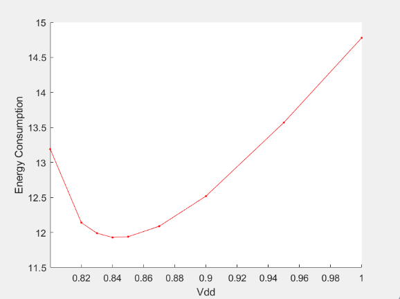
Figure 12. The relationship between energy consumption and  under
under 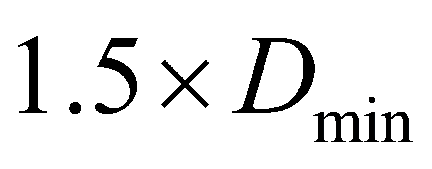 (Photo/Picture credit: Original).
As seen above, this paper finally finds that in the condition of 1.5  , the minimum energy consumption is 11.93W. Similarly, another nine group of data are processed, and find out the minimum energy consumption in the condition of different times of
  shown in table 6.
Table 6. The results of delay and energy consumption under different times of Dmin.
Dmin | D | E |
1.5Dmin | 95.955 | 11.93 |
1.4Dmin | 89.558 | 13.10 |
1.3Dmin | 83.161 | 14.43 |
1.2Dmin | 76.764 | 15.97 |
1.1Dmin | 70.367 | 17.89 |
1.05Dmin | 67.169 | 20.76 |
1.025Dmin | 65.570 | 25.11 |
1.0125Dmin | 64.770 | 29.32 |
1.01Dmin | 64.600 | 30.58 |
1.001Dmin | 64.030 | 39.84 |
Finally, the relationship of Delay and Energy Consumption can be drawn as below in figure 13.
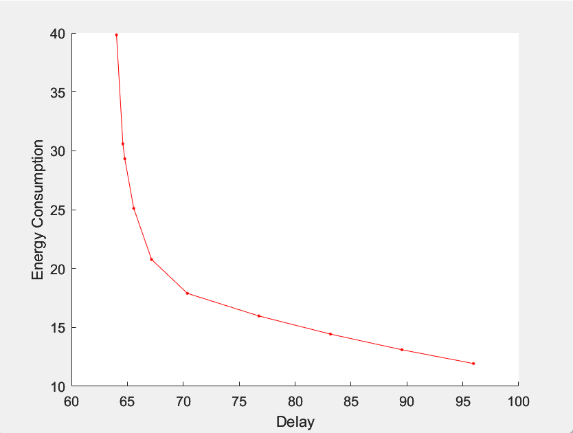
Figure 13. The relationship between and energy consumption (Photo/Picture credit: Original).
As shown above, this paper can conclude that as delay increases, the minimum energy consumption in the condition is significantly reduced. As a result, it’s an effective method to optimize circuit according to our need by changing the sizing and  of logic gates.
4. Conclusion
As a commonly used basic module, 4-bit absolute-value comparator plays a very important role in industry. In the first part, I mainly provide three ways to optimize the circuit, whether to use pure Boolean circuits or circuits with functional blocks, set the priority for logic gates, and use more appropriate number of stages in critical path. As a sophomore undergraduate, I chose this topic to study circuit design starting with a relatively simpler circuit topology of 4-bit absolute-value comparator, and use it as an example to establish a basic understanding of circuit design through exploration. Moreover, my purpose is to obtain more general methods and conclusions of circuit design by myself, and finally provide more ideas to solve design and optimization problems for you. So, I think the direction of the research of this project is very meaningful not only for me but also for the field. In the second part, I talked about how to optimize delay and energy consumption by changing the sizing and  . In terms of delay optimization, when the logic gates on the critical path satisfy
  , the delay is minimal.
In terms of energy consumption optimization, through nonlinear programming, the minimum energy with the delay of certain multiples of  is found, and the constraint relationship between delay and minimum energy is also verified. In short, although there is still a lot to improve and deepen in this project, it is a very valuable and challengeable experience for me and gives me a clearer plan for my future learning direction.
References
[1]. Lundstrom Mark, S and Alam Muhammad. “Moore’s law: The journey ahead, Science (New York, N.Y.) “. 2022, vol 378, no. 6621, pp. 722-723.
[2]. Chenyu Du, Yucheng Guo, Junchao Zhang. “A Low Energy Depletion CMOS Transistor-based 4-bit Absolute-value Detector”, Journal of Physics: Conference Series, 2023.
[3]. D. N. Mukherjee, S. Panda and B. Maji, “Design of low power 12-bit magnitude comparator,” 2017 Devices for Integrated Circuit (DevIC), Kalyani, India, 2017, pp. 103-109.
[4]. P. Das, P. J. Edavoor, S. Raveendran and A. D. Rahulkar, “Design and implementation of computationally efficient architecture of PID based motion controller for robotic land navigation system in FPGA,” 2017 Conference on Information and Communication Technology (CICT), Gwalior, India, 2017, pp. 1-6.
[5]. Chi-Chang Wang and Jin-Chuan Wu, “A 3.3-V/5-V low power TTL-to-CMOS input buffer,” in IEEE Journal of Solid-State Circuits, 1998, vol. 33, no. 4, pp. 598-603.
[6]. A. E. Engin, “Passive Multiport RC Model Extraction for Through Silicon Via Interconnects in 3-D ICs,” in IEEE Transactions on Electromagnetic Compatibility, 2014, vol. 56, no. 3, pp. 646-652.
[7]. S. Arora, P. T. Balsara and D. K. Bhatia, “Digital implementation of constant power load (CPL), active resistive load, constant current load and combinations,” 2016 IEEE Dallas Circuits and Systems Conference (DCAS), Arlington, TX, USA, 2016, pp. 1-4.
[8]. H. Rahman, C. Chakrabarti. “An efficient control point insertion technique for leakage reduction of scaled CMOS circuits”, IEEE Transactions on Circuits and Systems II: Express Briefs, 2005.
[9]. Akashi Satoh. “Unified Hardware Architecture for 128-Bit Block Ciphers AES and Camellia”, Lecture Notes in Computer Science, 2003.
[10]. Yung-Chih Chen. “Tree-Based Logic Encryption for Resisting SAT Attack”, 2017 IEEE 26th Asian Test Symposium (ATS), 2017.
Cite this article
Yan,R. (2024). Design and optimization of CMOS based 4-bit comparator. Applied and Computational Engineering,41,29-42.
Data availability
The datasets used and/or analyzed during the current study will be available from the authors upon reasonable request.
Disclaimer/Publisher's Note
The statements, opinions and data contained in all publications are solely those of the individual author(s) and contributor(s) and not of EWA Publishing and/or the editor(s). EWA Publishing and/or the editor(s) disclaim responsibility for any injury to people or property resulting from any ideas, methods, instructions or products referred to in the content.
About volume
Volume title: Proceedings of the 2023 International Conference on Machine Learning and Automation
© 2024 by the author(s). Licensee EWA Publishing, Oxford, UK. This article is an open access article distributed under the terms and
conditions of the Creative Commons Attribution (CC BY) license. Authors who
publish this series agree to the following terms:
1. Authors retain copyright and grant the series right of first publication with the work simultaneously licensed under a Creative Commons
Attribution License that allows others to share the work with an acknowledgment of the work's authorship and initial publication in this
series.
2. Authors are able to enter into separate, additional contractual arrangements for the non-exclusive distribution of the series's published
version of the work (e.g., post it to an institutional repository or publish it in a book), with an acknowledgment of its initial
publication in this series.
3. Authors are permitted and encouraged to post their work online (e.g., in institutional repositories or on their website) prior to and
during the submission process, as it can lead to productive exchanges, as well as earlier and greater citation of published work (See
Open access policy for details).
References
[1]. Lundstrom Mark, S and Alam Muhammad. “Moore’s law: The journey ahead, Science (New York, N.Y.) “. 2022, vol 378, no. 6621, pp. 722-723.
[2]. Chenyu Du, Yucheng Guo, Junchao Zhang. “A Low Energy Depletion CMOS Transistor-based 4-bit Absolute-value Detector”, Journal of Physics: Conference Series, 2023.
[3]. D. N. Mukherjee, S. Panda and B. Maji, “Design of low power 12-bit magnitude comparator,” 2017 Devices for Integrated Circuit (DevIC), Kalyani, India, 2017, pp. 103-109.
[4]. P. Das, P. J. Edavoor, S. Raveendran and A. D. Rahulkar, “Design and implementation of computationally efficient architecture of PID based motion controller for robotic land navigation system in FPGA,” 2017 Conference on Information and Communication Technology (CICT), Gwalior, India, 2017, pp. 1-6.
[5]. Chi-Chang Wang and Jin-Chuan Wu, “A 3.3-V/5-V low power TTL-to-CMOS input buffer,” in IEEE Journal of Solid-State Circuits, 1998, vol. 33, no. 4, pp. 598-603.
[6]. A. E. Engin, “Passive Multiport RC Model Extraction for Through Silicon Via Interconnects in 3-D ICs,” in IEEE Transactions on Electromagnetic Compatibility, 2014, vol. 56, no. 3, pp. 646-652.
[7]. S. Arora, P. T. Balsara and D. K. Bhatia, “Digital implementation of constant power load (CPL), active resistive load, constant current load and combinations,” 2016 IEEE Dallas Circuits and Systems Conference (DCAS), Arlington, TX, USA, 2016, pp. 1-4.
[8]. H. Rahman, C. Chakrabarti. “An efficient control point insertion technique for leakage reduction of scaled CMOS circuits”, IEEE Transactions on Circuits and Systems II: Express Briefs, 2005.
[9]. Akashi Satoh. “Unified Hardware Architecture for 128-Bit Block Ciphers AES and Camellia”, Lecture Notes in Computer Science, 2003.
[10]. Yung-Chih Chen. “Tree-Based Logic Encryption for Resisting SAT Attack”, 2017 IEEE 26th Asian Test Symposium (ATS), 2017.