


Introduction
In recent years, wearable sensors have been widely used. A typical device is a smartwatch. It can detect health data such as blood oxygen levels and heart rate through photoelectric sensors in it. In fact, many human physiological activities contain detectable electrical and magnetic signals. For instance, a professional doctor can determine a diagnosis based on the electrical activity of the heart through an electrocardiogram (ECG), while an electroencephalogram (EEG) is capable of recording the electrical signals of the brain with electrodes that are attached to the scalp. As an organ connected to the spinal cord, the brain is responsible for controlling almost every physiological function. Since EEG was first used to record the electrical activity of the brain in 1924, great progress has been made in this field. In the 1970s, the University of California, Los Angeles, began research on neuro-prosthetics, which also gave birth to the concept of Brain-Computer Interface [1]. BCIs are computer-based systems that allow communications between the brain and the machine and can analyse the brain’s signals or use them as feedback for instruments. The target population for this technology is usually medical patients who have severe motor dysfunction or cognitive impairments, such as locked-in syndrome (LiS) and Parkinson’s disease (PD) [2].
In this paper, the absolute-value detector (AVD) used to detect signals in BCIs will be discussed, including the design and optimisation. The design of the circuit will provide an academic justification of the topology and logic gate implementation, and optimisations will focus on the balance of energy and delay. The size of transistors and power supply voltage will be considered as two variables for the optimisation process. For the purpose of clarifying the importance of AVD in this field, it is necessary to explain the operating principle and application background of BCIs.
Principles of BCIs
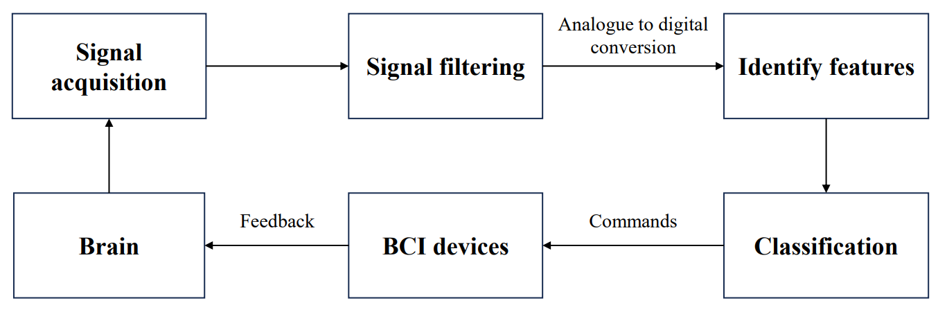
Similar to the working principle of most feedback systems, the operation mode of BCIs also require going through the basic steps of signal input, signal processing and signal output, as shown in figure 1. Obviously, the input signal here is the electrical or magnetic signal produced by the brain. In the signal processing part, these recorded signals need to be filtered, identified, and classified to generate the correct instructions to provide to the BCI device. In the modern healthcare system, devices for measuring brain signals are largely non-invasive. These devices consist of sensors placed on the scalp that measure the potential of an EEG or magnetoencephalography (MEG). Invasive devices are applied only in extreme cases and cannot avoid the risks of rejection reactions and neurosurgery itself. Therefore, semi-invasive devices that do not need to penetrate the cerebral cortex have been developed to reduce these risks. The typical signal that these devices can measure is the electrocorticography (ECoG). At present, BCIs still have limitations in the accuracy of signal acquisition. On the one hand, signals received by the sensor of a non-invasive device have passed a long distance and noise will inevitably mix in. On the other hand, due to the restriction of the number of electrodes, errors in sampled signals are possible for invasive techniques [3, 4]. If BCIs are to be applied more widely in healthcare, electromagnetic compatibility between electronic devices are also required to be considered, since there will be more than one device in the hospital room.
Figure 1. Operations of BCIs (Photo/Picture credit: Original). |
In order to accurately detect signals from the brain, spike-sorting is developed in chips for neural engineering [5]. It can record the spike of a large number of neurons simultaneously and separate the data of a single neuron to achieve classification function. In terms of hardware implementation, an AVD is one of the most suitable circuits for spike detection. AVDs can receive an input signal, usually in the form of 2’s complement, and then compare it to a threshold value. Therefore, an AVD consists of two portions: the transcoder and the comparator. The transcoder aims to extract the magnitude of the input while the comparator is used to make the comparison. The AVD has attached considerable research in recent years. Huang focused on using CMOS for logic gate design [6]. Carlson, Dewdney et al. selected a half-adder in the transcoder module and combined CMOS and pass-transistor logic (PTL) to reduce the number of transistors [7]. Jia designed a combinational logic circuit for transcoding and applied full adders to the comparator module [8]. On this basis, Jia proposed the possibility of transcoding with the truth table. However, these designs can be optimised in terms of fan-in. Du, Guo, Dong et al. increased the number of critical paths to compress the number of inputs of several logic gates [9, 10]. In fact, keeping the fan-in of a single gate below 4 can effectively reduce the delay. The objective of this paper is to propose a design and optimisation scheme of a 4-bit AVD, which uses truth tables and multiplexers for transcoding and focuses on the balance between delay and energy consumption. In addition, transmission gate logic (TGL) is considered for use in the structure of logic gates.
Design of the 4-bit AVD
This section covers the combinational logic circuit design of a 4-bit AVD. The output of the AVD should be logic 1 if the magnitude of its input signal is larger than that of the threshold level, otherwise the output is logic 0. Figure 2 shows the block diagram of an AVD.
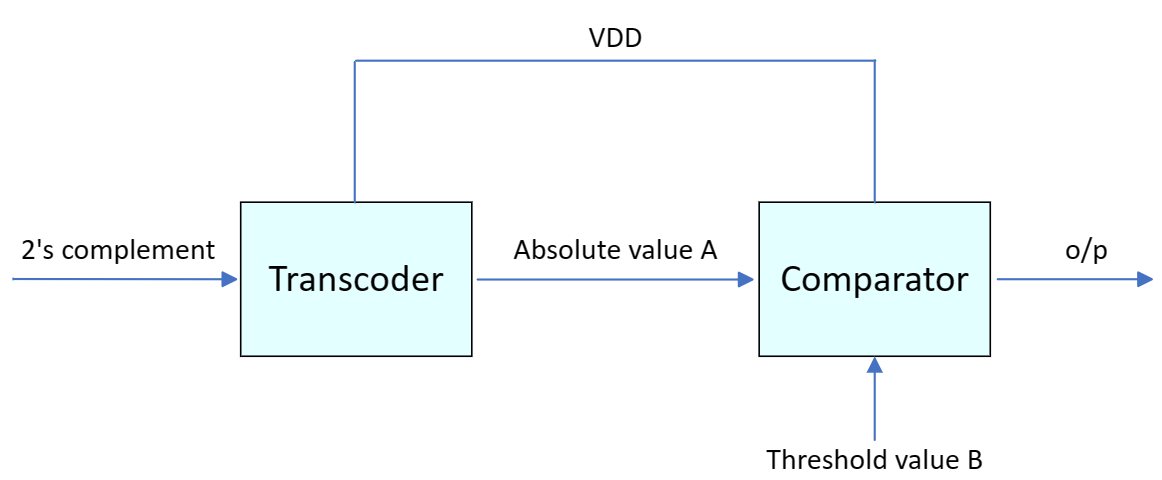
Figure 2. The block diagram of an AVD (Photo/Picture credit: Original).
Transcoder
The role of the transcoder is to identify the input signal and extract the absolute value. Since the input signal is composed of 2’s complement, the most significant bit (MSB) of input signals is the sign bit, which means the input ranges from -7 to +7 in decimal. When the MSB is logic 0, the positive input number can directly enter the comparator. When the MSB is logic 1, it indicates that the input number is negative and requires to be transcoded. Table 1 shows the truth table for negative inputs [11].
| X3 | X2 | X1 | X0 | A2 | A1 | A0 |
|---|---|---|---|---|---|---|
| 1 | 0 | 0 | 0 | 0 | 0 | 0 |
| 1 | 0 | 0 | 1 | 1 | 1 | 1 |
| 1 | 0 | 1 | 0 | 1 | 1 | 0 |
| 1 | 0 | 1 | 1 | 1 | 0 | 1 |
| 1 | 1 | 0 | 0 | 1 | 0 | 0 |
| 1 | 1 | 0 | 1 | 0 | 1 | 1 |
| 1 | 1 | 1 | 0 | 0 | 1 | 0 |
| 1 | 1 | 1 | 1 | 0 | 0 | 1 |
X3X2X1X0 is a 4-bit input and A2A1A0 represents the absolute value of corresponding inputs. X3 is 1 and it indicates negative numbers. From this table, logic functions of each output bit can be expressed as follows.
\[A_{0} = X_{0}\]
\[\begin{array}{r} A_{1} = X_{1} \oplus X_{0}\#(1) \end{array}\]
\[A_{2} = {\overline{X}}_{2} \cdot \left( X_{1} + X_{0} \right) + X_{2} \cdot \overline{X_{1}} \cdot \overline{X_{0}}\]
In addition, cases where X3 is 0 are also required to be considered. For positive inputs, their absolute values are identical to the last three bits. After combining these two conditions, multiplexers are selected to detect positive or negative numbers. Figure 3 shows the circuit design of the transcoder.
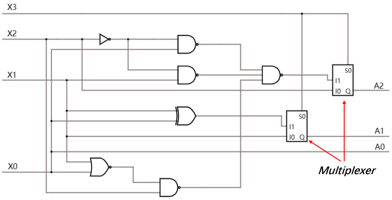
Figure 3. Logic circuit design of the transcoder (Photo/Picture credit: Original).
Comparator
The absolute value extracted by the transcoder is used as input to the comparator and then compared to a threshold value. Due to the removal of a sign bit, the comparator’s input will only be 3 bits. The output should be 1 if the input is higher than the threshold level, otherwise it should be 0. Table 2 shows the design principle of this comparator and the priority of individual bits.
| A2B2 | A1B1 | A0B0 | F(A>B) | F(A<B) |
|---|---|---|---|---|
| \[A_{2} > B_{2}\] | \(\ \times\)a | \[\times\] | 1 | 0 |
| \[A_{2} < B_{2}\] | \[\times\] | \[\times\] | 0 | 1 |
| \[A_{2} = B_{2}\] | \[A_{1} > B_{1}\] | \[\times\] | 1 | 0 |
| \[A_{2} = B_{2}\] | \[A_{1} < B_{1}\] | \[\times\] | 0 | 1 |
| \[A_{2} = B_{2}\] | \[A_{1} = B_{1}\] | \[A_{0} > B_{0}\] | 1 | 0 |
| \[A_{2} = B_{2}\] | \[A_{1} = B_{1}\] | \[A_{0} < B_{0}\] | 0 | 1 |
| \[A_{2} = B_{2}\] | \[A_{1} = B_{1}\] | \[A_{0} = B_{0}\] | 0 | 1 |
| a It means whatever the situation is, it will not affect the final output. | ||||
A2A1A0 is the input and the threshold value is B2B1B0. For the convenience of comparison, the MSBs of input and output are combined to determine whether they have an impact on the outcome. The result can be expressed as follows. Figure 4 is the circuit design of the comparator.
\[\begin{array}{r} F(A > B) = A_{2}\overline{B_{2}} + \left( A_{2} \odot B_{2} \right) \cdot A_{1}\overline{B_{1}} + \left( A_{2} \odot B_{2} \right)\left( A_{1} \odot B_{1} \right) \cdot A_{0}\overline{B_{0}}\#(2) \end{array}\]
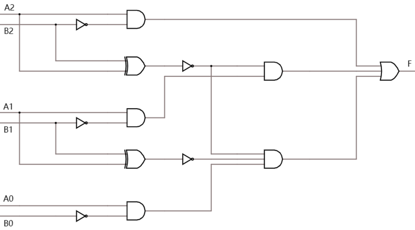
Figure 4. Logic circuit design of the comparator (Photo/Picture credit: Original).
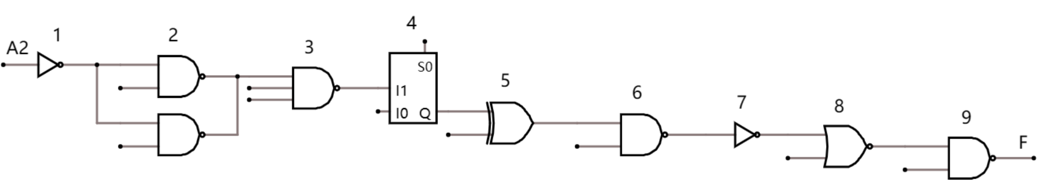
However, it is difficult to implement simple logic AND and OR in practice, and propagation delay deteriorates rapidly as a function of fan-in. As an alternative, NAND and NOR gates are used in place of simple logic gates. After simplification, the approved design that can be produced in the industry is shown in figure 5.
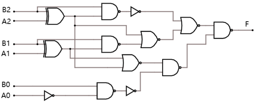
Figure 5. Approved design of the comparator (Photo/Picture credit: Original).
Logic implementations and Delay-energy Optimisation
In this section, technologies applied to implement the logic gates are illustrated. The delay and energy are calculated as well.
Implementations of logic gates and sizing
To obtain the longest delay of this circuit, the critical path that contains the largest number of logical gates is required. Figure 6 exhibits the critical path which contains totally 9 stages.
Figure 6. The critical path of the designed circuit (Photo/Picture credit: Original). |
The unit CMOS inverter consists of one PMOS transistor and one NMOS transistor. The width of a PMOS transistor is 650 nm and an NMOS transistor has a width of 430 nm. Both of them have a length of 100 nm. The difference of width between PMOS and NMOS is due to the mobility of carriers. Usually, the size of an inverter satisfies the condition that the resistances of PMOS and NMOS are identical, which represents the same delay of these two devices. For complex gates that have multiple transistors, it is necessary to size each transistor to maintain the same delay between pull-up network and pull-down network, referring to the unit inverter.
The propagation delay is mainly caused by the charging and discharging of intrinsic capacitors in the circuit. After defining the critical path, logical effort theory can be applied to calculate the delay. For this circuit, the assumption is that the input capacitance Cin of every input is equivalent to 2 unit-sized inverters, and the load capacitance CL is 32 times unit-sized inverters. The size of each transistor also reflects the capacitance. For a single logic gate, several definitions are shown below.
\[\begin{array}{r} g = \frac{C_{in,gate}}{C_{in,inv}},\ h = \frac{C_{L}}{C_{in}},\ p = \frac{C_{par,gate}}{C_{par,inv}}\#(3) \end{array}\]
Where g, h, and p are logical, electrical, and parasitic efforts respectively.
Figure 7 shows the implementation of NAND and NOR gates by CMOS technology.
Figure 7. The implementation of NAND and NOR gates by CMOS technology (Photo/Picture credit: Original). |
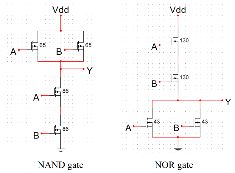
Figure 8 shows the implementation of multiplexers and XOR gates by TGL.
Figure 8. The implementation of multiplexers and XOR gates by TGL (Photo/Picture credit: Original). |
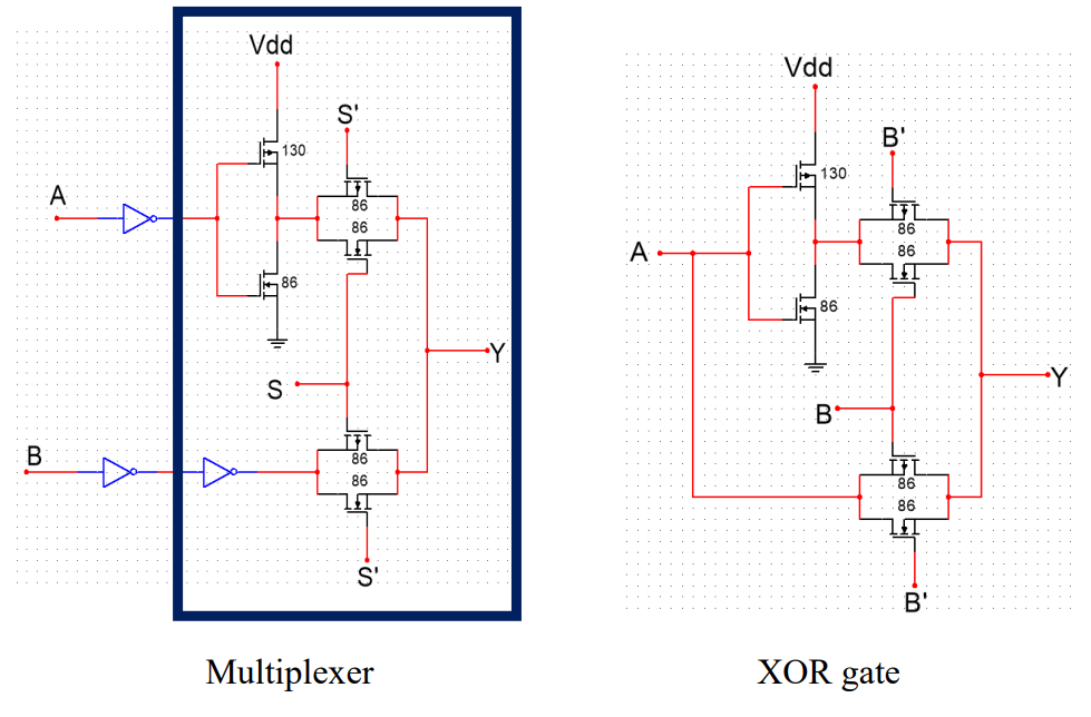
Table 3 calculates the key parameters for delay.
| Logic gate | Logical effort g | Parasitic effort p |
|---|---|---|
| NAND | 1.398 | 2 |
| NOR | 1.602 | 2 |
| MUX | 2 | 3.185 |
| XOR | 2.59 | 3.185 |
For the critical path, key parameters are defined as below.
\[\begin{array}{r} G = \Pi g_{i}\#(4) \end{array}\]
\[\begin{array}{r} H = \frac{C_{L}}{C_{in}}\#(5) \end{array}\]
Where G represents the pathway logical effort and H represents the pathway electrical effort.
Additionally, the branch path exists in the critical path and will affect the delay. The branching effort can be expressed as below.
\[\begin{array}{r} b = \frac{C_{onpath} + C_{offpath}}{C_{onpath}}\#(6) \end{array}\]
\[\begin{array}{r} B = \Pi b_{i}\#(7) \end{array}\]
\[\begin{array}{r} F = GBH\#(8) \end{array}\]
\[\begin{array}{r} f = \sqrt[N]{F}\#(9) \end{array}\]
Where b is branching effort, F is path effort, f is the optimal stage effort and N is the total number of stages. Therefore, the path delay can be obtained as D.
\[\begin{array}{r} D = Nf + \Sigma p_{i}\#(10) \end{array}\]
In terms of energy, the activity factor α0→1 of each stage should be calculated in advance. If the output of a logic gate is Y, then the activity factor can be calculated as below.
\[\begin{array}{r} \alpha_{0 \rightarrow 1} = P(Y = 0) \times P(Y = 1)\#(11) \end{array}\]
\[\begin{array}{r} S = \frac{C_{in}}{C_{out}}\#(12) \end{array}\]
Where P represents the probability of the output being a zero or one and S is the stage effort.
Ultimately, the energy of this path can be obtained.
\[\begin{array}{r} E = \alpha_{0 \rightarrow 1} \times \left( S_{i} + S_{i + 1} \right) \times C_{in} \times V_{DD}^{2}\#(13) \end{array}\]
Table 4 displays the initial results with the minimum delay when VDD is 1 V.
| Stage | 1 | 2 | 3 | 4 | 5 | 6 | 7 | 8 | 9 |
|---|---|---|---|---|---|---|---|---|---|
| g | 1 | 1.398 | 1.7962 | 2 | 2.59 | 1.398 | 1 | 1.602 | 1.398 |
| h | 2.590 | 1.849 | 1.443 | 1.370 | 1.438 | 1.851 | 2.604 | 1.624 | 1.850 |
| p | 1 | 2 | 3 | 3.185 | 3.185 | 2 | 1 | 2 | 2 |
| S | 2 | 2.59 | 4.79 | 6.91 | 5.05 | 2.21 | 4.09 | 10.65 | 17.3 |
| α0→1 | 0.25 | 0.1875 | 0.228 | 0.2445 | 0.25 | 0.1676 | 0.1676 | 0.2144 | 0.2288 |
| D | 3.590 | 4.585 | 5.591 | 5.926 | 6.909 | 4.587 | 3.604 | 4.602 | 4.586 |
| E | 1.148 | 1.593 | 3.400 | 3.925 | 2.105 | 1.215 | 2.470 | 6.560 | 12.984 |
The total delay is 43.98 and the energy is 35.4.
Optimisation of the delay and energy
In practice, the power consumption is an aspect that must be considered. Thus, the balance of delay and energy becomes the most critical part of integrated circuit design. For this circuit, the selected methodology is using supply voltage (VDD) scaling as variables to regulate the energy-delay curve. The range of supply voltage is from 0 to 1 V. When the delay grows to 1.5 times the original, stop changing the VDD and record the minimum energy at this moment. Microsoft Excel Solver can be used to simulate this model with the step of 0.05 times the minimum delay. Figure 9 is the connection between energy and delay with scaling VDD.
Figure 9. The relation between energy and delay with scaling VDD. (Photo/Picture credit: Original) |
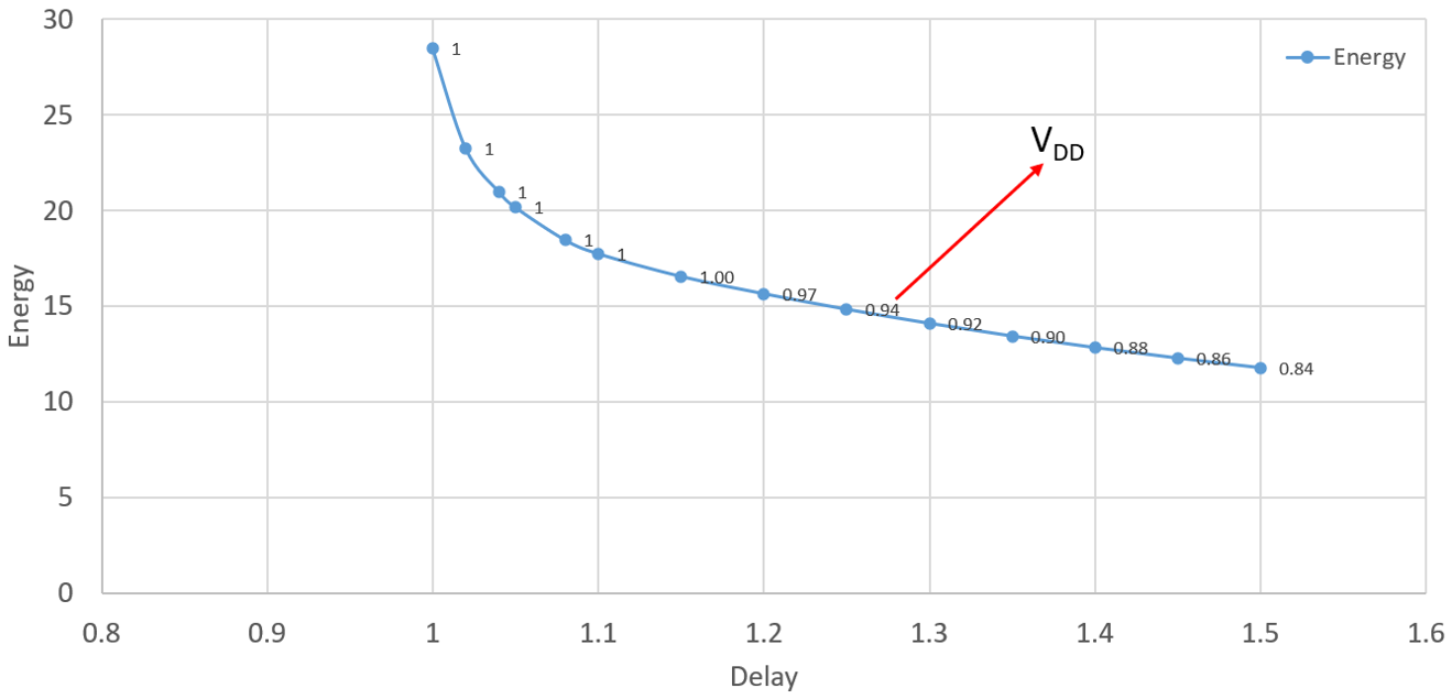
Table 5 shows the comparison of initial results and optimised results.
| Delay | Energy | VDD (V) | |
|---|---|---|---|
| Before scaling VDD | 43.98 | 35.4 | 1 |
| After scaling VDD | 65.97 | 11.76 | 0.8442 |
It can be summarised from the table that after scaling VDD, the circuit saved 67% energy and increased 50% delay.
Conclusion
In this paper, the structure of a 4-bit AVD was studied and designed. The logical effort theory was applied to calculate the delay and energy. The results showed that the energy consumption can be reduced by sacrificing the delay. With 1.5 times the minimum delay, this design saved 67% energy. It can be observed from the energy-delay curve that the energy consumption is suppressed with the increase of the delay. However, before the delay rises to 1.1 times, the energy decreases at a very rapid rate. Consequently, this range can bring huge benefits to the trade-off between the energy and delay.
This research provided a feasible design due to the abandonment of simple logic gates, and combined CMOS and TGL to reduce the number of transistors. Take the strict accuracy requirement of BCIs into consideration, AVDs in practical applications will certainly receive input signals far beyond 4 bits. Therefore, this design cannot meet the specifications of high-performance devices, but the research on the VDD scaling is still of great significance. The development of integrated circuits is extremely fast, and the current technology has been advanced to below 100 nm. The power supply has been reduced from traditional 5 V to below 1 V. For high-level integrated chip circuits, reducing power as much as possible while maintaining performance is the primary goal. Moreover, exploring and comparing various implementations of logic gates such as bipolar CMOS (BiCMOS) is a promising optimisation methodology.
References
[1]. J. R. Munavalli, P. R. Sankpal, A. Sumathi, and J. M. Oli, ‘Introduction to Brain–Computer Interface’, in Brain‐Computer Interface, Wiley, 2023, pp. 1–24.
[2]. M. A. Lebedev and M. A. L. Nicolelis, ‘Brain–machine interfaces: past, present and future’, Trends Neurosci, vol. 29, no. 9, pp. 536–546, Sep. 2006.
[3]. R. Portillo-Lara, B. Tahirbegi, C. A. R. Chapman, J. A. Goding, and R. A. Green, ‘Mind the gap: State-of-the-art technologies and applications for EEG-based brain-computer interfaces’, APL Bioeng, vol. 5, no. 3, p. 31507, Sep. 2021.
[4]. E. Mikołajewska and D. Mikołajewski, ‘Non-invasive EEG-based brain-computer interfaces in patients with disorders of consciousness’, Mil Med Res, vol. 1, no. 1, Jul. 2014.
[5]. A. Tankus, L. Solomon, Y. Aharony, A. Faust-Socher, and I. Strauss, ‘Machine learning algorithm for decoding multiple subthalamic spike trains for speech brain–machine interfaces’, J Neural Eng, vol. 18, no. 6, p. 066021, Nov. 2021.
[6]. Z. Huang, ‘Performance Optimization of 4-bit Absolute Value Detector Based on Structural Design’, J Phys Conf Ser, vol. 2435, no. 1, 2023.
[7]. B. R. Carlson, P. E. Dewdney, and T. A. Burgess, ‘Design and Optimization of A 4-bit Absolute-value Detector Using Half Adder and Comparator’, J Phys Conf Ser, vol. 2435, no. 1, p. 012009, Feb. 2023.
[8]. Y. Jia, ‘Design and Optimization of 4-bit Absolute-value Detector Based on CMOS’, J Phys Conf Ser, vol. 2435, no. 1, p. 012011, Feb. 2023.
[9]. C. Du, Y. Guo, and J. Zhang, ‘A Low Energy Depletion CMOS Transistor-based 4-bit Absolute-value Detector’, J Phys Conf Ser, vol. 2435, no. 1, p. 012012, Feb. 2023.
[10]. X. Dong, B. Jing, and X. Yang, ‘Improved Design of a 4-bit Absolute-Value Detector Using Simplified Chain Carry Adder’, J Phys Conf Ser, vol. 2113, no. 1, p. 012043, Nov. 2021.
[11]. A. Jain, A. Singh, S. Singhal, A. Mudgal, and A. Mehra, ‘A Novel Power Efficient 2:4 Decoder at 16nm’, 2021 International Conference on Computer Communication and Informatics, ICCCI 2021, Jan. 2021.
Cite this article
Zhou,Y. (2024). A methodology of designing and optimising a 4-bit absolute-value detector for the application of Brain-computer Interface. Applied and Computational Engineering,42,263-272.
Data availability
The datasets used and/or analyzed during the current study will be available from the authors upon reasonable request.
Disclaimer/Publisher's Note
The statements, opinions and data contained in all publications are solely those of the individual author(s) and contributor(s) and not of EWA Publishing and/or the editor(s). EWA Publishing and/or the editor(s) disclaim responsibility for any injury to people or property resulting from any ideas, methods, instructions or products referred to in the content.
About volume
Volume title: Proceedings of the 2023 International Conference on Machine Learning and Automation
© 2024 by the author(s). Licensee EWA Publishing, Oxford, UK. This article is an open access article distributed under the terms and
conditions of the Creative Commons Attribution (CC BY) license. Authors who
publish this series agree to the following terms:
1. Authors retain copyright and grant the series right of first publication with the work simultaneously licensed under a Creative Commons
Attribution License that allows others to share the work with an acknowledgment of the work's authorship and initial publication in this
series.
2. Authors are able to enter into separate, additional contractual arrangements for the non-exclusive distribution of the series's published
version of the work (e.g., post it to an institutional repository or publish it in a book), with an acknowledgment of its initial
publication in this series.
3. Authors are permitted and encouraged to post their work online (e.g., in institutional repositories or on their website) prior to and
during the submission process, as it can lead to productive exchanges, as well as earlier and greater citation of published work (See
Open access policy for details).
References
[1]. J. R. Munavalli, P. R. Sankpal, A. Sumathi, and J. M. Oli, ‘Introduction to Brain–Computer Interface’, in Brain‐Computer Interface, Wiley, 2023, pp. 1–24.
[2]. M. A. Lebedev and M. A. L. Nicolelis, ‘Brain–machine interfaces: past, present and future’, Trends Neurosci, vol. 29, no. 9, pp. 536–546, Sep. 2006.
[3]. R. Portillo-Lara, B. Tahirbegi, C. A. R. Chapman, J. A. Goding, and R. A. Green, ‘Mind the gap: State-of-the-art technologies and applications for EEG-based brain-computer interfaces’, APL Bioeng, vol. 5, no. 3, p. 31507, Sep. 2021.
[4]. E. Mikołajewska and D. Mikołajewski, ‘Non-invasive EEG-based brain-computer interfaces in patients with disorders of consciousness’, Mil Med Res, vol. 1, no. 1, Jul. 2014.
[5]. A. Tankus, L. Solomon, Y. Aharony, A. Faust-Socher, and I. Strauss, ‘Machine learning algorithm for decoding multiple subthalamic spike trains for speech brain–machine interfaces’, J Neural Eng, vol. 18, no. 6, p. 066021, Nov. 2021.
[6]. Z. Huang, ‘Performance Optimization of 4-bit Absolute Value Detector Based on Structural Design’, J Phys Conf Ser, vol. 2435, no. 1, 2023.
[7]. B. R. Carlson, P. E. Dewdney, and T. A. Burgess, ‘Design and Optimization of A 4-bit Absolute-value Detector Using Half Adder and Comparator’, J Phys Conf Ser, vol. 2435, no. 1, p. 012009, Feb. 2023.
[8]. Y. Jia, ‘Design and Optimization of 4-bit Absolute-value Detector Based on CMOS’, J Phys Conf Ser, vol. 2435, no. 1, p. 012011, Feb. 2023.
[9]. C. Du, Y. Guo, and J. Zhang, ‘A Low Energy Depletion CMOS Transistor-based 4-bit Absolute-value Detector’, J Phys Conf Ser, vol. 2435, no. 1, p. 012012, Feb. 2023.
[10]. X. Dong, B. Jing, and X. Yang, ‘Improved Design of a 4-bit Absolute-Value Detector Using Simplified Chain Carry Adder’, J Phys Conf Ser, vol. 2113, no. 1, p. 012043, Nov. 2021.
[11]. A. Jain, A. Singh, S. Singhal, A. Mudgal, and A. Mehra, ‘A Novel Power Efficient 2:4 Decoder at 16nm’, 2021 International Conference on Computer Communication and Informatics, ICCCI 2021, Jan. 2021.