


1. Introduction
Throughout the annals of technological history, certain inventions have punctuated our journey, marking not only significant shifts in the way we live but also symbolizing major eras. Mention fire, the wheel, or the printing press, and one can immediately recognize the huge progress they introduced, and the societal and cultural changes linked with them. In our current times, the transistor holds such a distinguished position. While it might not have the elemental allure of fire, its widespread impact on our daily lives is palpable.
The transistor, more than just a semiconductor component, is the foundation of the digital age. From its early days with the bipolar junction transistor to the application of Metal-Oxide-Semiconductor Field-Effect Transistors (MOSFETs), Fin Field-Effect Transistors (FinFETs), and now Gate-All-Around Field-Effect Transistors (GAAFETs), these components have been the cornerstone of modern technology's growth. This paper dives into a comprehensive narrative of the transistor's development, exploring the principles that make it work, and illustrating how it has powered the technological wonders of our age. Our discussion will encompass its inception, the use of materials enhancing its efficiency, its crucial role in the miniaturization of electronic devices, and the leaps from MOSFET to FinFET to GAAFET in improving transistor performance.
For those of us living in this era, understanding the role of the transistor isn't just about quenching our technological thirst. It’s a lesson in the sheer potential of innovation. It reminds us that even the smallest and simplest technologies can drive monumental change. And while we might only be speculating about the future of transistors at this point, this paper hopes to provide a foundation for envisioning the next steps in transistor evolution.
2. Evolution of FET Architectures: From MOSFETs to GAAFETs
Over the years, transistor technologies have undergone significant advancements to meet the ever-increasing demands of the electronics industry. This section delves into the evolutionary journey of Field-Effect Transistors, starting from the traditional MOSFET, moving to the 3D structured FinFET, and finally to the latest gate-all-around GAAFET. We will explore the mechanisms, structures, and challenges associated with each technology.
2.1. MOSFET
The Metal-Oxide-Semiconductor Field-Effect Transistor (MOSFET) is a vital component in the evolution of electronic devices. It uses a metal gate, insulating oxide layer, and semiconductor material to modulate the flow of current by varying the voltage applied to the gate terminal.
The MOSFET concept was first proposed in the early 20th century, but it was Julius Edgar Lilienfeld who patented the idea in the 1920s. Yet, it wasn't until the 1960s that Dawon Kahng and Martin M. Atalla at Bell Labs fabricated the first working device [1].
A MOSFET operates through the application of voltage at its gate, which creates an electric field. This field either attracts carriers, inducing a conductive channel (enhancement mode) or repels carriers, depleting the channel (depletion mode). The underlying physics is largely dependent on the PN junction dynamics, where a P-type (positive) and N-type (negative) semiconductor are joined, leading to a depletion region. By manipulating this region with an external voltage, one can control the conductivity between the source and drain terminals [2].
To elucidate further, consider the fundamental difference between the two primary types of MOSFETs: pMOS and nMOS. These variants differ mainly in the type of carriers (holes or electrons) that participate in conduction and their electrical properties. A comparative diagram of pMOS and nMOS is shown in Figure 1.

Figure 1. Comparative structures of pMOS and nMOS transistors.
2.2. FINFET
The Fin Field-Effect Transistor (FinFET) represents an evolutionary leap from the traditional MOSFET. It adopts a three-dimensional "fin" shaped silicon structure extending above the substrate, offering enhanced electrostatic control. The comparison is shown in Figure 2.
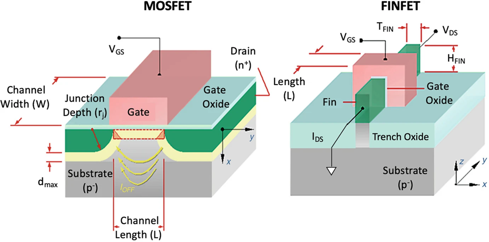
Figure 2. Structural comparison between MOSFET and FinFET
The journey of multi-gate devices culminated in 1999 when Chenming Hu introduced the "FinFET," short for Fin Field Effect Transistor, marking a significant milestone by cramming a record number of transistors onto a chip. This technological advancement was driven by the challenges faced by planar MOSFETs, especially at the deep sub-micron scales [3].
While the basic principle remains the same as in MOSFETs – controlling the flow of current between the source and drain through the gate voltage – the key difference lies in their structure. A traditional MOSFET is a planar structure, where the gate is located on top of the channel. In contrast, a FinFET uses a 3D fin-like structure that rises above the plane of the substrate. The gate wraps around this fin from two or even three sides, allowing for better electrostatic control of the channel.
2.3. GAAFET
The figure 3 illustrates the evolution in design and structure of the FET architecture over the years.
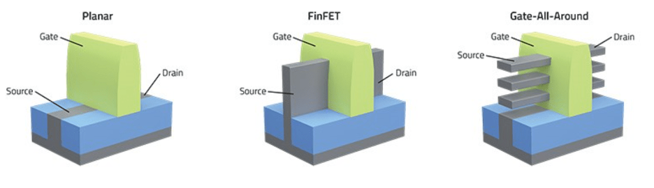
Figure 3. Comparative structures of MOSFET, FinFET, and GAAFET.
Gate-All-Around Field-Effect Transistor (GAAFET) is distinct in its structure, where the gate material surrounds the channel from all angles, leading to unprecedented electrostatic control [4].
GAAFETs, while being a forefront technology today, have their roots set back in 1988. A Toshiba research team, comprising of Fujio Masuoka, Hiroshi Takato, and Kazumasa Sunouchi, made a groundbreaking demonstration of a vertical nanowire GAAFET, which they termed as a "surrounding gate transistor" [5].
The unique structure of GAAFET, with its gate enveloping the channel, results in a superior electrostatic environment. This configuration minimizes short-channel effects drastically, even as device dimensions shrink. Unlike traditional FETs where the electrostatic control is from one or two sides, the GAAFET ensures a near-uniform potential profile across the channel, allowing for very steep sub-threshold slopes, thereby enabling low voltage operation. This translates to faster switching, better threshold voltage stability, and much-reduced leakage currents, making GAAFETs highly efficient even in their quiescent state [4].
2.4. Comparison
The dimension or size of MOSFETs, traditionally planar in structure, has consistently been miniaturized over the decades, reaching physical limitations due to short-channel effects and quantum tunneling. This size limitation paved the way for FinFETs, introducing a 3D "fin" structure that provided improved control and allowed for further scaling, pushing beyond the restrictions that planar MOSFETs faced. As people approach the atomic scale, even FinFETs begin to encounter challenges, leading to the rise of GAAFETs. GAAFETs, with their gate-all-around structure, promise even more aggressive scaling while maintaining exceptional electrostatic control, offering a glimpse into the future of transistor evolution.
Traditional planar MOSFETs, as they scaled down, faced increasing challenges with leakage current due to short-channel effects, adversely impacting power efficiency. The advent of FinFETs, with their distinctive 3D 'fin' structures, provided better gate control, significantly reducing off-state leakage and enhancing power efficiency. As technology progresses to even smaller nodes, GAAFETs come into the spotlight. With their gate-all-around structure, GAAFETs offer superior electrostatic control over the channel, achieving further reductions in leakage and pushing the boundaries of power efficiency in semiconductor devices.
As transistor dimensions continue to scale down, the challenges associated with Threshold Voltage (Vth) and Short Channel Effect (SCE) have become increasingly critical. For traditional planar MOSFETs, maintaining a stable threshold voltage becomes arduous with size reduction due to pronounced SCEs, leading to Vth variability, increased leakage currents, threshold voltage roll-off, and DIBL (Drain-Induced Barrier Lowering). The advent of FinFETs, with their 3D structure, offered enhanced gate control over their planar counterparts, especially at smaller nodes, mitigating many of the Vth and SCE related issues to some extent. However, as the dimensions of FinFETs continue to shrink, they aren't entirely exempt from SCEs. In contrast, GAAFETs, with their gate-all-around configuration, provide almost unparalleled control against SCEs. The all-encompassing gate structure of GAAFETs ensures a uniform potential profile across the channel, drastically minimizing SCEs and thereby guaranteeing consistent device performance at the forefront of transistor technology.
3. Expanding Horizons: Applications Across FET Generations
The evolution of Field-Effect Transistors (FETs) has paved the way for an extensive range of applications, revolutionizing industries and fostering technological leaps in diverse sectors. As FET architectures have advanced, their integration into electronic systems has expanded and transformed to accommodate the specific benefits and features of each FET generation. This section explores the multitude of applications across different FET types, showcasing how MOSFETs, FinFETs, and GAAFETs have influenced and shaped various domains of electronics.
3.1. MOSFET Applications
In the realm of power electronics and drive systems, the modern push towards faster, more efficient, and compact systems has seen the pivotal integration of MOSFETs, alongside IGBTs, for switching and regulating current. Especially in high-frequency operations, these transistors help reduce switching losses, a major source of power loss in semiconductor switches. Consequently, MOSFET drivers have been designed to activate the transistors rapidly. Furthermore, Power MOSFETs, built specifically for managing large currents or power, are frequently employed in switching power supplies and motor controllers [6].
Shifting focus to digital logic and processing, MOSFETs control conductivity, which is essential to digital logic. They can function as switches, controlling other circuits or transistors, laying the foundation for computational logic. Moreover, the integration of MOSFETs onto chips makes them indispensable elements of modern Central Processing Units (CPUs) and Graphics Processing Units (GPUs). With advancements, MOSFET designs have shrunk to a few nanometers, supporting the continued realization of Moore's law [7].
In the domain of computer memory, older Static Random-Access Memory (SRAM) relies on the state of a MOSFET in a flip-flop arrangement to store binary data. Meanwhile, modern Dynamic Random-Access Memory (DRAM) uses the charge of a MOS capacitor, an offshoot of MOSFET technology, for data storage. Not to forget, EEPROM, EPROM, and contemporary flash memories employ floating gate MOSFETs as storage units [7].
Lastly, when it comes to sensing and imaging, both the earlier charge-coupled device (CCD) technology and the modern CMOS active-pixel sensors harness the charge produced by a photon, which is stored by a MOS capacitor and later read by an integrated circuit. Expanding its applications, MOS technology is also making its mark in the world of biological and chemical sensing [7].
3.2. FinFET Applications
The advent of FinFET technology has brought about transformative applications across various domains of electronics. One prominent application is in low power digital logic systems. A study by Jaisawal et al. explored the potential of Negative Capacitance FinFET (NC-FinFET) for such applications [8]. Compared to traditional FinFETs, NC-FinFETs exhibited a reduced delay across certain operating frequencies, leading to substantial power savings. This efficiency makes NC-FinFETs an attractive choice for power-conscious applications, including specific circuits like embedded inverter chains, three-stage ring oscillators (ROs), and 2-bit ripple carry adders (RCAs).
Diving into memory and Artificial Intelligence (AI) realms, the paper by Gul et al. introduces the idea of compute-in-memory (CIM) as an innovative solution to address data traffic challenges in AI systems employing deep neural networks (DNNs) [9]. Notably, FinFET-based 6T-SRAM cells are emphasized for their fit in CIM architectures, marking a significant transition from planar transistors to the advanced 3D-FinFET structure. This transition has paved the way for enhancements in design density, power conservation, and overall performance.
Lastly, in the context of computational applications, the design of the 1-bit FinFET sum circuit emerges as a focal point. Pittala & Vijay's paper delves into this design, which holds pivotal importance in digital systems such as microprocessors and digital signal processing [10]. The research accentuates the role of full adders in these digital platforms, pointing out the capability of FinFET technology in designing a 1-bit sum circuit that not only saves power but also reduces delay and minimizes chip area requirements.
3.3. GAAFET Applications
GAAFET technology, known for its exceptional electrostatic control, is carving a niche in various electronics domains. One primary area of application is in high-performance computing (HPC) and servers. With its innate power efficiency and capability for performance enhancement, GAAFET emerges as a fitting choice for state-of-the-art central processing units (CPUs). These CPUs, leveraging the attributes of GAAFET, can clock higher frequencies while conserving power. Such traits are invaluable for data centers and servers that operate under the dual constraints of energy efficiency and heavy computational needs.
Moving to the realm of ultra-low power devices, GAAFET’s inherent power-saving characteristic combined with its ability to function at minimal voltages becomes particularly pivotal for Internet of Things (IoT) devices and wearables. Such devices, often constrained by battery capacities, find GAAFET-based designs to be a boon, ensuring longer battery life without diminishing performance.
Additionally, in the evolving landscape of memory technologies, GAAFET's attributes are becoming invaluable. Memory forms like Magnetoresistive Random-Access Memory (MRAM) and Resistive Random-Access Memory (ReRAM) can benefit from the energy efficiency and reduced leakage that GAAFETs provide. Kumar et al. specifically illustrated the potential of a GAAFET-based SRAM cell to enhance stability and performance metrics for low power applications [11]. This synergy points towards future memory solutions that cater to both standalone and integrated applications.
On the frontier of artificial intelligence, the exponential growth and intricacy of deep learning models necessitate hardware capable of supporting intensive computations. GAAFETs, renowned for their superior switching speeds, are becoming integral in hardware accelerators tailored for neural networks and expansive machine learning operations. This adaptability can notably enhance the efficacy of devices at the edge running complex AI algorithms.
Lastly, in the realm of communication, especially with the emergence of 5G, GAAFETs are showing significant promise. The escalating demand for rapid data transmission calls for transistors with the agility to function at escalated frequencies while curbing power use. Kumar et al. proposed a DM-HD-NA GAAFET structure that not only reduces DIBL but is also suitable for RF applications due to its enhanced electrostatic and tunnelling characteristics [12]. These attributes suggest that GAAFETs, with their stellar electrostatic control and minimized leakage, can play pivotal roles in RF transceivers and 5G modems. Their structural advantages hint at their potential as the linchpin in the forthcoming generation of communication apparatuses.
4. Beyond the Surface: Challenges and Opportunities in FET Progression
The relentless march of semiconductor technology has not been without its roadblocks. As the industry constantly evolves, transcending traditional boundaries and adopting newer architectures, it confronts a plethora of challenges. Concurrently, the inherent dynamism of this sector spawns opportunities, beckoning novel advancements that could redefine the very fabric of electronics. This section delves into the intricacies of the challenges posed by transistor evolution and the prospective advancements waiting on the horizon.
4.1. Challenges in Transistor Evolution
The transition from MOSFETs to FinFETs and now to GAAFETs heralds a bright future for electronic technologies. Yet, inherent challenges accompany this evolution.
As we strive for further miniaturization of transistors, approaching atomic scales, the current capabilities of lithography and fabrication methods come into question. It becomes imperative to find innovative ways to ensure precision at these scales. Concurrently, the compact design leads to difficulties in efficient heat dissipation, with devices potentially facing elevated temperatures. This heat can detrimentally influence both performance and durability.
Another concern arises from leakage and variability. Despite the advancements, as dimensions reduce, issues like electron tunnelling and leakage become increasingly prominent. Moreover, variations introduced during manufacturing can cause inconsistent performance across transistors.
Shifting focus to materials, the development and incorporation of new or mixed materials for advanced transistors might necessitate fresh approaches to ensure compatibility with existing semiconductor processes.
Furthermore, as the scales get smaller, transistors might become more susceptible to wear-out mechanisms such as hot carrier injection, bias temperature instability, and time-dependent dielectric breakdown.
Diving deeper into the atomic realm brings forth quantum effects. Phenomena like quantum tunnelling become more significant, leading to uncertainties in transistor behaviour. Specifically, quantum tunnelling can cause unforeseen current flows even when the transistor is turned off, introducing challenges in maintaining energy efficiency and device reliability.
4.2. Prospective Development Beyond GAAFET in Future Transistors
The world of semiconductor technology has witnessed a swift progression, from MOSFETs to the forefront GAAFETs. Despite these advancements, the industry continues its relentless pursuit of even more efficient, smaller transistors. Projecting the developments beyond GAAFETs, certain directions of innovations seem to be emerging.
Harnessing alternative materials to the traditionally dominant silicon stands out as a promising venture. Studies, like the one by Das et al., have suggested Germanium (Ge) as a material with potential to enhance electrostatic properties of transistors [13]. Moreover, future pathways might gravitate towards 2D materials, such as graphene or transition metal dichalcogenides (TMDCs). These materials promise benefits like superior electron mobility and enhanced channel control, which are vital for advancing transistor technology. Another aspect of innovation focuses on architectural changes. With the continuous reduction in transistor dimensions, new designs are vital to maintain peak performance. Noteworthy is the emergence of U-shaped Field-Effect Transistors [13]. These designs are believed to offer a smaller gate footprint and minimize leakage, proposing them as potential successors to prevailing architectures.
On the design horizon, hybrid models are emerging. For example, the complementary Field-Effect Transistor (CFET) is an architectural innovation where n- and pMOS devices are integrated vertically [14]. This design eliminates the traditional n-p spacing from cell height considerations, thereby enhancing the effective channel width and drive current. As the world evolves beyond GAAFETs, such integrative designs might define the transitional phase, hinting at the future of transistors.
5. Conclusion
The rapid progression of transistor technologies, from MOSFETs to FinFETs and on to GAAFETs, undeniably paints a promising picture for the future of electronic devices and systems. Yet, with advancement comes an array of challenges, spanning size constraints, thermal issues, leakage concerns, and manufacturing consistency. Moreover, interfacing with existing systems and the adoption of new materials present hurdles in both compatibility and reliability. Nevertheless, the trajectory of technological evolution remains optimistic. The exploration of alternative materials, such as Germanium and 2D materials, may play a pivotal role in future developments. Additionally, diversification in architecture, showcased by innovations like U-shaped FETs and CFETs, hints at the potential successors to traditional GAA-FETs. In essence, while challenges persist, the semiconductor realm is characterized by unceasing innovation, and we can anticipate even more efficient and compact transistor technologies emerging in the future.
References
[1]. Charboneau T. Fathers of the MOSFET: Dawon Kahng and Martin Atalla. All About Circuits. 2021.
[2]. Teja R. Introduction to MOSFET | Enhancement, Depletion, Amplifier, Applications. Electronics Hub. 2021.
[3]. Chung H T, Shih B J, Yang C C, et al. Ge Single-Crystal-Island (Ge-SCI) Technique and BEOL Ge FinFET Switch Arrays on Top of Si Circuits for Monolithic 3D Voltage Regulators. 2021 IEEE International Electron Devices Meeting (IEDM). IEEE, 2021: 34.5. 1-34.5. 4.
[4]. Erin Z. Semiconductor Engineering. Gate-All-Around FET (GAA FET)- A possible replacement transistor design for finFETs. 2023.
[5]. Li Y, Kanazawa K, Izawa T, et al. 1.5-nm node surrounding gate transistor (SGT)-SRAM cell with staggered pillar and self-aligned process for gate, bottom contact, and pillar. 2021 IEEE International Memory Workshop (IMW). IEEE, 2021: 1-4.
[6]. Pathak AD. MOSFET/IGBT drivers theory and applications. Application Note AN002. 2001.
[7]. Wright G. Metal-oxide semiconductor field-effect transistor (MOSFET). TechTarget. 2023.
[8]. Jaisawal R K, Kondekar P N, Yadav S, et al. Insights into the operation of negative capacitance FinFET for low power logic applications. Microelectronics Journal, 2022, 119: 105321.
[9]. Gul W, Shams M, Al-Khalili D. FinFET 6T-SRAM All-Digital Compute-in-Memory for Artificial Intelligence Applications: An Overview and Analysis. Micromachines, 2023, 14(8): 1535.
[10]. Pittala C, Vijay V. Design of 1-Bit FinFET sum circuit for computational applications. International Conference on Emerging Applications of Information Technology. Singapore: Springer Singapore, 2021: 590-596.
[11]. Kumar A, Pattanaik M, Srivastava P, et al. GAAFET based SRAM Cell to Enhance Stability for Low Power Applications. Silicon, 2022, 14(13): 8161-8172.
[12]. Kumar A, Pattanaik M, Srivastava P, et al. Reduction of Drain Induced Barrier Lowering in DM‐HD‐NA GAAFET for RF Applications. IET Circuits, Devices & Systems, 2020, 14(3): 270-275.
[13]. Das U K, Bhattacharyya T K. Opportunities in device scaling for 3-nm node and beyond: FinFET versus GAA-FET versus UFET. IEEE transactions on electron devices, 2020, 67(6): 2633-2638.
[14]. Imec Z. Imec puts complementary FET (CFET) on the logic technology roadmap. Imec-int. 2023.
Cite this article
Duan,H. (2024). From MOSFET to FinFET to GAAFET: The evolution, challenges, and future prospects. Applied and Computational Engineering,50,113-120.
Data availability
The datasets used and/or analyzed during the current study will be available from the authors upon reasonable request.
Disclaimer/Publisher's Note
The statements, opinions and data contained in all publications are solely those of the individual author(s) and contributor(s) and not of EWA Publishing and/or the editor(s). EWA Publishing and/or the editor(s) disclaim responsibility for any injury to people or property resulting from any ideas, methods, instructions or products referred to in the content.
About volume
Volume title: Proceedings of the 4th International Conference on Signal Processing and Machine Learning
© 2024 by the author(s). Licensee EWA Publishing, Oxford, UK. This article is an open access article distributed under the terms and
conditions of the Creative Commons Attribution (CC BY) license. Authors who
publish this series agree to the following terms:
1. Authors retain copyright and grant the series right of first publication with the work simultaneously licensed under a Creative Commons
Attribution License that allows others to share the work with an acknowledgment of the work's authorship and initial publication in this
series.
2. Authors are able to enter into separate, additional contractual arrangements for the non-exclusive distribution of the series's published
version of the work (e.g., post it to an institutional repository or publish it in a book), with an acknowledgment of its initial
publication in this series.
3. Authors are permitted and encouraged to post their work online (e.g., in institutional repositories or on their website) prior to and
during the submission process, as it can lead to productive exchanges, as well as earlier and greater citation of published work (See
Open access policy for details).
References
[1]. Charboneau T. Fathers of the MOSFET: Dawon Kahng and Martin Atalla. All About Circuits. 2021.
[2]. Teja R. Introduction to MOSFET | Enhancement, Depletion, Amplifier, Applications. Electronics Hub. 2021.
[3]. Chung H T, Shih B J, Yang C C, et al. Ge Single-Crystal-Island (Ge-SCI) Technique and BEOL Ge FinFET Switch Arrays on Top of Si Circuits for Monolithic 3D Voltage Regulators. 2021 IEEE International Electron Devices Meeting (IEDM). IEEE, 2021: 34.5. 1-34.5. 4.
[4]. Erin Z. Semiconductor Engineering. Gate-All-Around FET (GAA FET)- A possible replacement transistor design for finFETs. 2023.
[5]. Li Y, Kanazawa K, Izawa T, et al. 1.5-nm node surrounding gate transistor (SGT)-SRAM cell with staggered pillar and self-aligned process for gate, bottom contact, and pillar. 2021 IEEE International Memory Workshop (IMW). IEEE, 2021: 1-4.
[6]. Pathak AD. MOSFET/IGBT drivers theory and applications. Application Note AN002. 2001.
[7]. Wright G. Metal-oxide semiconductor field-effect transistor (MOSFET). TechTarget. 2023.
[8]. Jaisawal R K, Kondekar P N, Yadav S, et al. Insights into the operation of negative capacitance FinFET for low power logic applications. Microelectronics Journal, 2022, 119: 105321.
[9]. Gul W, Shams M, Al-Khalili D. FinFET 6T-SRAM All-Digital Compute-in-Memory for Artificial Intelligence Applications: An Overview and Analysis. Micromachines, 2023, 14(8): 1535.
[10]. Pittala C, Vijay V. Design of 1-Bit FinFET sum circuit for computational applications. International Conference on Emerging Applications of Information Technology. Singapore: Springer Singapore, 2021: 590-596.
[11]. Kumar A, Pattanaik M, Srivastava P, et al. GAAFET based SRAM Cell to Enhance Stability for Low Power Applications. Silicon, 2022, 14(13): 8161-8172.
[12]. Kumar A, Pattanaik M, Srivastava P, et al. Reduction of Drain Induced Barrier Lowering in DM‐HD‐NA GAAFET for RF Applications. IET Circuits, Devices & Systems, 2020, 14(3): 270-275.
[13]. Das U K, Bhattacharyya T K. Opportunities in device scaling for 3-nm node and beyond: FinFET versus GAA-FET versus UFET. IEEE transactions on electron devices, 2020, 67(6): 2633-2638.
[14]. Imec Z. Imec puts complementary FET (CFET) on the logic technology roadmap. Imec-int. 2023.