


1. Introduction
In the development of modern computers, the operation speed and energy consumption of chips are two crucial factors. With the increase in the number of chip transistors, Moore’s Law is gradually becoming less effective, posing new challenges for chip development [1]. To enhance computing power, chip companies have begun exploring new technological directions. Among them, hardware reconstruction has emerged as a new design approach [2]. By reconstructing circuits and logic units, chips can become more flexible, efficient, and better adapted to different application scenarios [3].
The objective of this paper is to design a low-latency, low-power 4-bit absolute value detector using CMOS transistors with minimal materials and simplified structures. This detector is capable of taking the absolute value of an input, comparing it with a threshold value, and outputting 1 if the absolute value of the input exceeds the threshold or 0 if it falls below. Consequently, this paper encompasses the design of both an absolute value module and a comparator module, as well as the implementation of techniques such as introducing delay and reducing supply voltage to minimize detector energy consumption [4]. Utilizing conventional design methodologies, we have analyzed and developed a 4-bit absolute value detector with a delay of 92.4FO4 (1V) and an energy consumption of 53.71Eu (1V). This detector boasts moderate dimensions and rapid operational speeds. Modern chips contain a plethora of modules, and the 4-bit absolute value detector is just one of them. By optimizing the structure and simplifying the circuit through the methods presented in this paper, it may significantly enhance the operational efficiency of chips.
2. Design of 4-bit absolute value detector circuit
2.1. Principle of logical value
Firstly, based on the function of the absolute value detector, the input 4-bit binary number with signed bits needs to be analyzed. When the highest bit is 1, the input value is negative, and when the highest bit is 0, the input value is positive. If the input is positive, the input value will not be changed, and if the input is negative, the input value will be changed to its opposite [5]. In addition, the decimal form of the 4-bit binary number with signed bits can represent values from -8 to 7, and its truth table is shown in Table 1 below.
Table 1. Truth table
The binary number of the input | decimal number | The binary number of the input | decimal number |
1000 | -8 | 0000 | 0 |
1001 | -7 | 0001 | 1 |
1010 | -6 | 0010 | 2 |
1011 | -5 | 0011 | 3 |
1100 | -4 | 0100 | 4 |
1101 | -3 | 0101 | 5 |
1110 | -2 | 0110 | 6 |
1111 | -1 | 0111 | 7 |
By analyzing the table above, it can be seen that to take the absolute value of a negative number, it is necessary to first invert the four digits of the input negative number, followed by adding 1.
2.2. Absolute module
According to the principle of logical values, it can be analyzed that the function of adding 1 to the four-digit number after negating it in this design needs to be completed by a selector module and an adder module. First, since the input value is a signed four-digit number and the output is an unsigned three-digit number, and the positive and negative values of the input value are controlled by the sign bit X3. Therefore, three 2:1 MUX are selected, which are controlled by the sign bit X3 for flipping. If X3 is 1, that is, the input value is negative, then the opposite value of the remaining three bits is output. If X3 is 0, that is, the input value is positive, then the remaining three digits are output [6]. For the adder part, we considered many types of adders, such as super-fast carry adder, bypass carry adder, and so on. However, due to the relatively simple process of adding 1 to the three-digit number, there is no complex carry calculation. Therefore, this article chooses to complete the addition operation by three series of half adders, whose logical expression is shown in formula 1. Here, Y2Y1Y0 is the output value of the input value X2X1X0 after processing by the absolute value module. C0 and C1 are the carry numbers generated during this operation.
 (1)
(1)
These two parts combine to form a logic value module as shown in Figure 1, which is used to determine the positive or negative value of the input and output its absolute value [7].
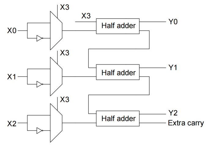
Figure 1. Absolute module (Picture credit: Original)
2.3. Comparator module
To implement the function of a 4-bit absolute value detector, after obtaining the 3-bit absolute value of the input value, a comparator module is also required to be designed to compare it with the input threshold value [8]. If the absolute value is greater than the threshold value, then output 1, otherwise output 0. Therefore, the comparison value module satisfies the following logical expression. Where Z is the threshold value representing the input. And Y2Y1Y0 is the output value of the input value X2X1X0 after processing by the absolute value module.
 (2)
(2)
The operation logic of the comparator is shown in the following table 2.
Table 2. Comparator operation logic
Y2Z2 | Y1Z1 | Y0Z0 | F(Y>Z) |
Y2>Z2 | neglect | neglect | 1 |
Y2<Z2 | neglect | neglect | 0 |
Y2=Z2 | Y1>Z1 | neglect | 1 |
Y2=Z2 | Y1<Z1 | neglect | 0 |
Y2=Z2 | Y1=Z1 | Y0>Z0 | 1 |
Y2=Z2 | Y1=Z1 | Y0<Z0 | 0 |
Y2=Z2 | Y1=Z1 | Y0=Z0 | 0 |
To implement this logical expression, the comparison module is designed as shown in the figure 2 below.
This structure enables the comparison module to compare Y0Y1Y2 with the input threshold values Z0Z1Z2 in order from high to low. When the high-order Y>Z, the result is directly output without further comparison of the low-order values. When the high-order Y=Z, the comparison continues with the low-order values until the result is output. In summary, this structure has fewer logic gate elements than traditional comparison units, and can also shorten the comparison time and reduce energy consumption. The comparison logic is shown in the following figure 2 [9].
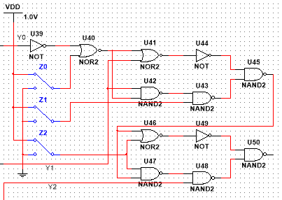
Figure 2. Comparator module (Picture credit: Original)
2.4. Optimization of circuit structure
Due to the ease of manufacturing and design of NAND, NOR, and NOT gates, as well as the convenience of standardized operations, they are needed to replace other logic gates in the design process. At the same time, multiple logic gate structures in the circuit, as shown in the figure 3 below, can be transformed into simpler single logic gates. And the transformation therapy is shown below.
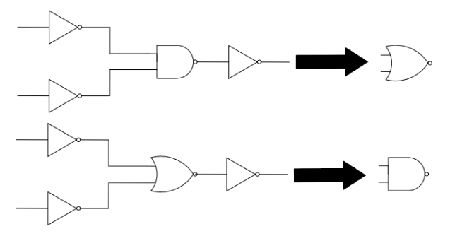
Figure 3. Transformation therapy (Picture credit: Original)
After transformation, a shorter and lower-latency circuit structure will be obtained. After analyzing the logic value principle, combining the absolute value module and comparison module, and optimizing, the circuit diagram in this article will have fewer logic gates, lower latency, and be more conducive to computation [10].
2.5. Main circuit
The main circuit diagram after combining the absolute value module and comparison module and optimizing the structure is shown in the figure 4.
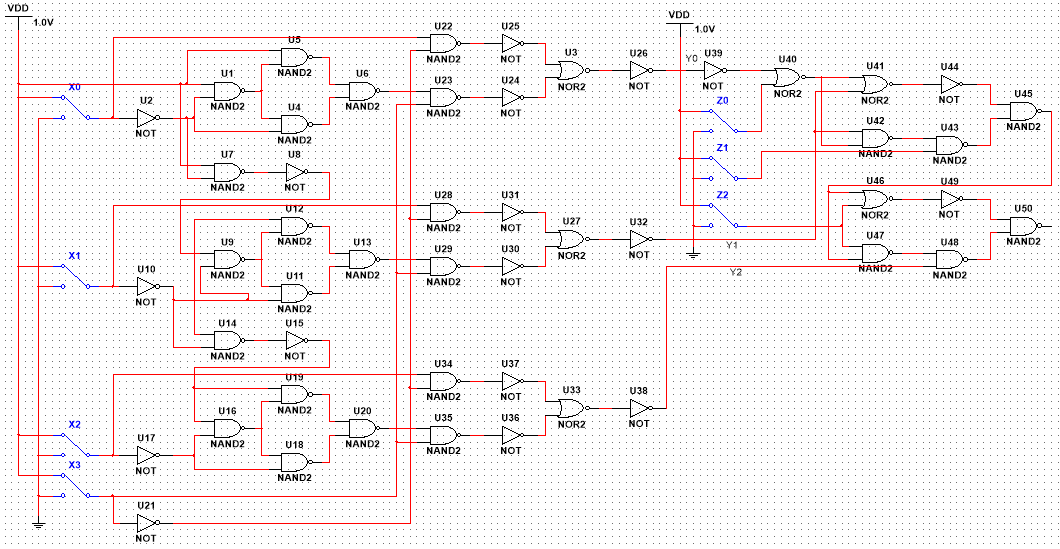
Figure 4. Main circuit (Picture credit: Original)
The flowchart of the operation steps of the 4-bit absolute value detector designed in this article is shown in the figure 5 below.
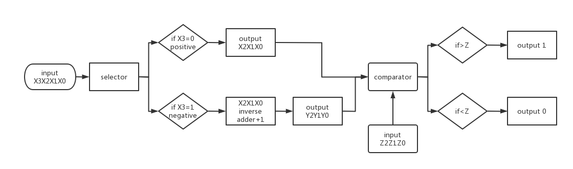
Figure 5. Flow chart (Picture credit: Original)
3. Parameter calculation
After completing the design and structural optimization of the main circuit, this section aims to find a better solution for the power consumption and delay of the 4-bit absolute value detector through optimizing the power supply. Therefore, it is necessary to first calculate key path delays, energy consumption, and other parameters.
In the project requirements, the unit size of the inverter is Wp=650nm, Wn=430nm, and the ratio of Wp to Wn is approximately 1.5. First, calculate the logic effort g and parasitic effort p under this ratio.
After calculation, the g and p values for the AND, NAND, and NOR gates required in this design are shown in the following table.
Table 3 Path parasitic delay
g | p | |
NOR | 1.6 | 2 |
NAND | 1.4 | 2 |
NOT | 1 | 1 |
Next, the shortest and most effective path in the main loop is selected as the critical path. The original and simplified diagrams of the critical path are shown in figure 6 below. From the diagram, there are 16 logic gates selected as critical.
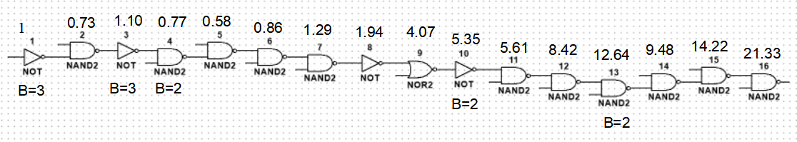
Figure 6. Critical path (Picture credit: Original)
Based on the calculated logic effort g and parasitic effort p of the logic gates, the path logic effort G can be generated:
 (3)
(3)
Path electrical effort can be generated:
 (4)
(4)
Here, Cout(path) is the capacitance at the end of the path, and Cin(path) is the capacitance at the beginning of the path.
Path branch effort can be generated:
 (5)
(5)
Path effort can be generated:
 (6)
(6)
 (7)
(7)
Path parasitic delay can be generated:
 (8)
(8)
Total path delay can be generated:
 (9)
(9)
After calculating the total effect, it is necessary to calculate the size of the logic gates on the critical path.
Use the following formula to calculate the path effect and optimal stage effect.
 (10)
(10)
 (11)
(11)
Gate sizing can be calculated by this formula:
 (12)
(12)
The dimensions of logic gates on the critical path are shown in the following table 4.
Table 4. Each Cin
Sequence | 1 | 2 | 3 | 4 | 5 | 6 | 7 | 8 |
Cin | 1 | 0.73 | 1.10 | 0.77 | 0.58 | 0.86 | 1.29 | 1.94 |
9 | 10 | 11 | 12 | 13 | 14 | 15 | 16 | |
4.07 | 5.35 | 5.61 | 8.42 | 12.64 | 9.48 | 14.22 | 21.33 |
The calculation of energy E in this article can be based on the following formula.
 (13)
(13)
The current energy E can be obtained as 89.425.
4. Optimization
In order to reduce the energy consumption of the circuit, there are two methods to reduce energy consumption. One is to reduce the supply voltage, and the other is to change the size of the logic gate. This article will explain the specific details of the voltage reduction method.
Use the method of increasing the delay by 1.5 times in the task requirements to reduce energy consumption, while maintaining the logic gate size unchanged.
Firstly, the delay follows the following relationship.
 (14)
(14)
Here VT=0.2V, as mentioned above, D is 61.6, then the increased delay is:

Therefore, the optimized VDD is:
 (15)
(15)
Substituting this into the calculation, we can obtain the optimized VDD as 0.775V.
At the same time, the energy consumption after optimizing the power supply is:
 (16)
(16)
The change ratio of energy consumption is:
 (17)
(17)
Through this method, the energy consumption is reduced by nearly 40%.
5. Conclusion
This article uses truth tables and logical expressions to analyze in detail the functions that the detector needs to implement, and designs its absolute value module and comparison module based on this. At the same time, it optimizes its structure, using only NOR, NAND, NOT logic gates, resulting in fewer logic gates in the overall circuit, lower delay, and easier calculation. Finally, after calculating key parameters such as critical path delay and energy consumption, we reduce the power supply voltage by increasing the delay by 1.5 times, resulting in a reduction in energy consumption of the absolute value detector by approximately 40%.
However, this article does not optimize the dimensions of logic gates. If the optimization process includes changing the dimensions of logic gates and reducing the supply voltage, it will result in optimal delay and energy consumption. Secondly, this article only optimizes key routes, not the entire system. Therefore, it may be beneficial to use MATLAB for global optimization in the future.
References
[1]. Waldrop M M. The chips are down for Moore’s law. Nature News, 2016, 530(7589): 144.
[2]. Korcyl G, Białas P, Curceanu C, et al. Evaluation of single-chip, real-time tomographic data processing on FPGA SoC devices. IEEE transactions on medical imaging, 2018, 37(11): 2526-2535.
[3]. Wang P, Gao F, **g Y, et al. An integrated gate driver with active delay control method for series connected SiC MOSFETs. 2018 IEEE 19th Workshop on Control and Modeling for Power Electronics (COMPEL). IEEE, 2018: 1-6.
[4]. Wada K, Shingu K. Voltage balancing control for series connected MOSFETs based on time delay adjustment under start-up and steady-state operations. 2018 IEEE Energy Conversion Congress and Exposition (ECCE). IEEE, 2018: 5495-5499.
[5]. Chen H, Hossain M M, Castillo D G, et al. Design and optimization of SiC MOSFET wire bondless power modules. 2020 IEEE 9th international power electronics and motion control conference (IPEMC2020-ECCE Asia). IEEE, 2020: 725-728.
[6]. Shur M, Fjeldly T A, Ytterdal T, et al. Unified MOSFET model. Solid-state electronics, 1992, 35(12): 1795-1802.
[7]. Sakurai T, Newton A R. Delay analysis of series-connected MOSFET circuits. IEEE Journal of Solid-State Circuits, 1991, 26(2): 122-131.
[8]. Nagaraju V S, Babu P A, Ratna V R, et al. Design and implementation of low power 32-bit comparator. Proceedings of the International Conference on IoT Based Control Networks and Intelligent Systems (ICICNIS 2020), Palai, India. 2020: 459-468.
[9]. Khorami A, Sharifkhani M. A low-power high-speed comparator for precise applications. IEEE Transactions on Very Large Scale Integration (VLSI) Systems, 2018, 26(10): 2038-2049.
[10]. Mallick S, Kar R, Mandal D, et al. Optimal sizing of CMOS analog circuits using gravitational search algorithm with particle swarm optimization. International Journal of Machine Learning and Cybernetics, 2017, 8: 309-331.
Cite this article
Huang,Z. (2024). A [92.4] FO4(1V), [53.71] Eu(1V) 4-bit absolute-value detector. Applied and Computational Engineering,65,89-96.
Data availability
The datasets used and/or analyzed during the current study will be available from the authors upon reasonable request.
Disclaimer/Publisher's Note
The statements, opinions and data contained in all publications are solely those of the individual author(s) and contributor(s) and not of EWA Publishing and/or the editor(s). EWA Publishing and/or the editor(s) disclaim responsibility for any injury to people or property resulting from any ideas, methods, instructions or products referred to in the content.
About volume
Volume title: Proceedings of Urban Intelligence: Machine Learning in Smart City Solutions - CONFSEML 2024
© 2024 by the author(s). Licensee EWA Publishing, Oxford, UK. This article is an open access article distributed under the terms and
conditions of the Creative Commons Attribution (CC BY) license. Authors who
publish this series agree to the following terms:
1. Authors retain copyright and grant the series right of first publication with the work simultaneously licensed under a Creative Commons
Attribution License that allows others to share the work with an acknowledgment of the work's authorship and initial publication in this
series.
2. Authors are able to enter into separate, additional contractual arrangements for the non-exclusive distribution of the series's published
version of the work (e.g., post it to an institutional repository or publish it in a book), with an acknowledgment of its initial
publication in this series.
3. Authors are permitted and encouraged to post their work online (e.g., in institutional repositories or on their website) prior to and
during the submission process, as it can lead to productive exchanges, as well as earlier and greater citation of published work (See
Open access policy for details).
References
[1]. Waldrop M M. The chips are down for Moore’s law. Nature News, 2016, 530(7589): 144.
[2]. Korcyl G, Białas P, Curceanu C, et al. Evaluation of single-chip, real-time tomographic data processing on FPGA SoC devices. IEEE transactions on medical imaging, 2018, 37(11): 2526-2535.
[3]. Wang P, Gao F, **g Y, et al. An integrated gate driver with active delay control method for series connected SiC MOSFETs. 2018 IEEE 19th Workshop on Control and Modeling for Power Electronics (COMPEL). IEEE, 2018: 1-6.
[4]. Wada K, Shingu K. Voltage balancing control for series connected MOSFETs based on time delay adjustment under start-up and steady-state operations. 2018 IEEE Energy Conversion Congress and Exposition (ECCE). IEEE, 2018: 5495-5499.
[5]. Chen H, Hossain M M, Castillo D G, et al. Design and optimization of SiC MOSFET wire bondless power modules. 2020 IEEE 9th international power electronics and motion control conference (IPEMC2020-ECCE Asia). IEEE, 2020: 725-728.
[6]. Shur M, Fjeldly T A, Ytterdal T, et al. Unified MOSFET model. Solid-state electronics, 1992, 35(12): 1795-1802.
[7]. Sakurai T, Newton A R. Delay analysis of series-connected MOSFET circuits. IEEE Journal of Solid-State Circuits, 1991, 26(2): 122-131.
[8]. Nagaraju V S, Babu P A, Ratna V R, et al. Design and implementation of low power 32-bit comparator. Proceedings of the International Conference on IoT Based Control Networks and Intelligent Systems (ICICNIS 2020), Palai, India. 2020: 459-468.
[9]. Khorami A, Sharifkhani M. A low-power high-speed comparator for precise applications. IEEE Transactions on Very Large Scale Integration (VLSI) Systems, 2018, 26(10): 2038-2049.
[10]. Mallick S, Kar R, Mandal D, et al. Optimal sizing of CMOS analog circuits using gravitational search algorithm with particle swarm optimization. International Journal of Machine Learning and Cybernetics, 2017, 8: 309-331.