


1. Introduction
Long wave infrared detector detection wavelength of 8.0-14μm. For room temperature or lower temperature detection, it can obtain greater signal energy, so it is suitable for room temperature and low temperature detection activities. After a lot of practice, it is found that the long wave infrared detector has high transmittance, can provide superior target recognition ability for complex environment and poor visibility conditions, and has good universality.
In the last three decades, there has been a significant evolution in infrared detectors, especially in the military and commercial domains. A key advancement in this area is the development of the InAs/GaSb Tape Binary II Superlattice, recognized for its pivotal role in Third-Generation Infrared Focal Plane Arrays detectors [1]. Its outstanding material properties include a tunable band gap from 0 to 0.8ev, broad wavelength sensitivity, elevated quantum efficiency, decreased Auger recombination, and low dark current. This study zeroes in on examining an InAs/GaSb Superlattice (SL) infrared detector with a variable wavelength response. The research includes refining the SL manufacturing techniques and conducting an in-depth exploration and analysis of its material characteristics, thus playing a significant role in enhancing infrared detection technology [2].
2. Development History of InAs/GaSb Superlattice (SL) infrared detector
In a seminal contribution to the field of infrared detection technology, Northwestern University reported the development of the first InAs/GaSb Class II superlattice long/long wave two-color detector in 2011. This detector, a 320×256 array, demonstrated cutoff wavelengths at 9.5 µm and 13 µm, respectively, and achieved a noise equivalent temperature difference (NETD) of approximately 20 mK in both bands. Progressing further, Northwestern University unveiled an advanced version in 2012, featuring a larger array size of 640x512 with a pixel pitch of 30 µm [3]. This enhanced model registered NETDs of 15 mK and 20 mK in the red and blue channels, respectively, at a temperature of 81K.
In a parallel development, Raytheon Company in the United States introduced a long/long wave mercury cadmium telluride (MCT) infrared detector array. This array, sized at 512×512, exhibited cutoff wavelengths ranging from 7.0 to 8.5 µm and 10.0 to 11.5 µm. It displayed a dark current density at 70 K comparable to that of liquid phase epitaxial monochromatic long-wave MCT detectors, approximately 10-6 A/cm2 [4].
In 2019, the Chinese Academy of Sciences’ Institute of Semiconductors announced a significant breakthrough with the development of the nipin type laminated long/long wave two-color unit infrared detector. However, the application of superlattice long/long dichroic infrared focal plane detectors in China remains unreported [5]. A comparative analysis reveals that Antimony-based Class II superlattices offer several advantages over traditional mercury cadmium telluride detectors. These include a reduction in dark current, enhanced process stability, and a decrease in material flaws. These benefits are particularly pronounced in applications involving long wave and very long wave bands, underscoring the potential of these superlattices in next-generation infrared detection technologies.
3. Optimization Method Analysis
3.1. Temperature optimization
Contemporary research in semiconductor fabrication has underscored the pivotal role of temperature in influencing the growth rate, quality, and surface flatness of Group III elements on substrates. This study delves into the intricate relationship between temperature and epitaxial growth dynamics. It is observed that excessively low temperatures can impede the growth rate, leading to the formation of peak and valley structures on the surface. Conversely, beyond a certain threshold, an increase in temperature paradoxically results in a decreased growth rate, adversely impacting the formation of the stepped growth layers, which are central to this research. The focal point of this investigation is the effect of growth temperature on the epitaxial buffer layer of GaSb.
3.1.1. InAlAs metamorphic buffer layers grown at different temperature gradients. Figure 1 shows the 20 μm × 20 μm AFM images of the InAlAs metamorphic buffer layers grown at different temperature gradients. Clear cross-hatch morphology can be seen on all sample surfaces under the low magnification, which is the typical surface morphology of metamorphic epi-structure. This cross-hatch morphology is typically seen in zinc-blende structures in lattice-mismatched III-V semiconductor heterostructures. It is caused by two different kinds of misfit dislocations (MDs), which are located along the [1–10] and [110] directions, respectively, and are thought to have group V and group III atom-based cores. As observed in Figure 1, the three samples’ major ridges run parallel to each other along the [1–10] direction [6]. Oval-shaped undulations then appear on top of the primary ridges, creating subsidiary ridges and valleys with shorter periods along the [110] direction.
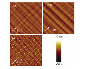
Figure 1. AFM images of the InAlAs metamorphic buffer layers grown at different temperature gradients [6]
In this study, the network of misfit dislocations (MDs) is represented through a crosshatch pattern model. The focus of the analysis is on the non-uniform strain induced by MDs at the growth front, which leads to the preferential deposition of Aluminum (Al) and Indium (In) atoms. This phenomenon subsequently results in variations in both the thickness and alloy composition of the materials. Furthermore, the surface roughness of the samples is attributed to the large-scale cross-hatch pattern, which is further compounded by small-scale three-dimensional features, such as dots and mounds.
Quantitatively, the root-mean-square (RMS) roughness values for samples A1, A2, and A3 have been measured at 2.2 nm, 3.4 nm, and 3.6 nm, respectively. These findings suggest a correlation between the increase in the growth temperature gradient and the incremental rise in the surface roughness of the samples. This study aims provide a deeper understanding of the impact of growth conditions on the physical characteristics of the materials, particularly focusing on the effects of MD-induced strain and temperature gradients on surface topography.
3.1.2. Optimization of growth temperature of GaSb buffer. In the realm of semiconductor fabrication, the present investigation focuses on the impact of substrate epitaxial buffer layer growth temperature on the properties of the GaSb buffer layer. The study acknowledges the significant influence of growth temperature on the reconstructed surface of GaSb buffer layers, emphasizing the necessity of identifying an optimal growth temperature for GaSb, which is shown in figure 2.
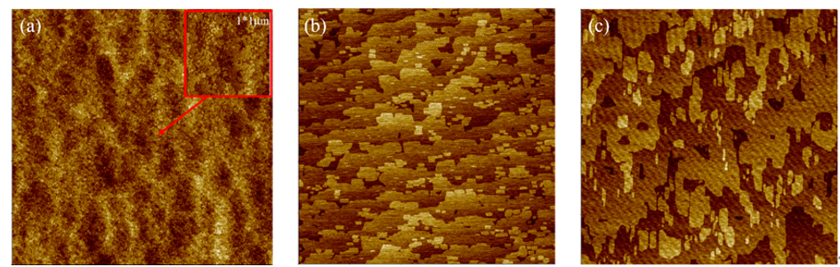
Figure 2. Surface topography of the 5×5µm microregion characterized by AFM at different temperatures [7]. (a) The epitaxial growth temperature is 440℃ (b) epitaxial growth temperature of 460℃ (c) The epitaxial growth temperature was 465℃
It is noted that the epitaxial growth temperatures for InAs and GaSb materials differ; GaSb typically requires a higher temperature range for optimal growth, generally between 440°C and 500°C, in contrast to the growth temperature for InAs. The objective of this research is to delineate the effects of varying growth temperatures on the morphological and structural characteristics of the GaSb buffer layer, thereby enabling the optimization of growth conditions for enhanced material quality and performance in semiconductor applications. Finally, after observation and comparison with AFM, it found that in the epitaxy process of GaSb buffer layer, excessive Group V atoms produce Group III vacancies at low temperatures, acting as non-composite centers, so the defect density of materials growing at lower temperatures may be higher, so the growth temperature should be appropriately increased. This means that GaSb buffer layer epitaxial layer surface quality is better at 460 ° C [7].
3.2. Optimization of stream flux of group V/Ⅲ elements
Benyahia D research investigates the impact of varying V/III beam flux ratios on the epitaxial layer quality, specifically focusing on InAs/GaSb superlattices [8]. Through experimental analysis, it was found that the InAs V/III ratio has a profound effect on both the strain and surface quality of these superlattices. A notable discovery was that an InAs V/III ratio set at 7 resulted in the least surface roughness. Building on this discovery, the study then fine-tunes the InAs V/III ratio to this optimal level. Utilizing results from Atomic Force Microscopy (AFM) and High-Resolution X-Ray Diffraction (HRXRD), the research suggests that a GaSb V/III ratio of 2 could lead to a higher quality structure. The objective of this study is to deepen the understanding of how V/III beam flux ratios influence the epitaxial growth of InAs/GaSb superlattices, aiming to enhance semiconductor manufacturing techniques.
Selection and optimization of superlattice interfaces Research and selection of suitable superlattice interfaces: Interface chemistry is determined by complex exchange, mixing and separation effects and is extremely important for their optimization. InAs/GaSb superlattice Due to the continuous alternating growth of InAs and GaSb, about 0.6% strain exists in InAs (6.0584 A) and GaSb (6.0959 A) in a single period [8]. In order to enhance the absorption of the infrared detector, the thickness of the superlattice absorption region must be increased to a few microns. If the strain in the cycle is not limited, with the increase of the growth cycle, the strain gradually accumulates, and eventually the stress is released through the dislocation, resulting in a fatal impact on the quality of the entire superlattice. Fortunately, in the experiment, the 0.6% strain can be compensated by controlling the interface type between the superlattice layers, and the overall strain of the superlattice can be balanced.
3.3. Selection and optimization of superlattice interface
3.3.1. Superlattice interface selection: In the growth process, due to the different valve switching sequence of the source furnace, there are two growth sequences of InAs layer and GaSb layer, and these two different sequences will lead to two different interface types, namely InSb-like and GaAs-like. In epitaxy, the lattice mismatch between InAs and GaSb layers is often balanced by introducing InSb layers, and the superlattices with InSb layers have better optical properties. The selection of barrier layer and growth layer is shown in figure 3 [9].
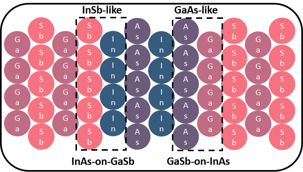
Figure 3. Selection of barrier layer and growth layer [9]
For device performance testing, we evaluate the optoelectronic properties of the devices through I-V testing, photocurrent response testing, blackbody testing, etc. This allows us to obtain important parameters such as dark current, differential impedance area, device spectral response, quantum efficiency, and detection rate. These parameters are used to optimize the material growth and device fabrication processes [10].
3.4. Execution
3.4.1. The preparation process of InAs/GaSb Class II. Superlattice materials is shown in the figure 4 below.
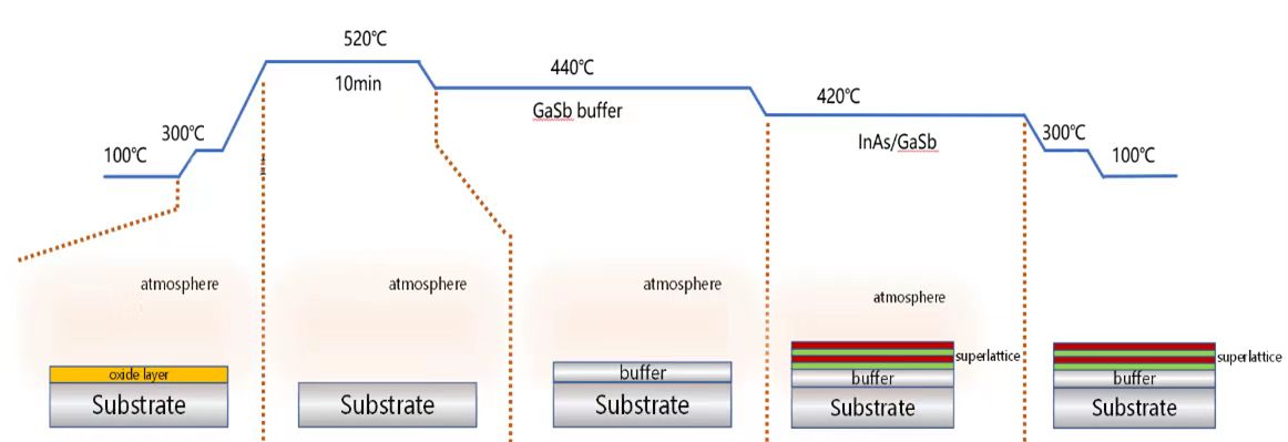
Figure 4. Preparation flow chart of superlattice materials [11]
The initial stage depicted involves the treatment of the substrate with an oxide layer at 100°C, followed by a temperature increase to 300°C. Subsequently, the temperature is further raised to 520°C and maintained for 10 minutes to facilitate the formation of a gas buffer layer. The middle section illustrates the deposition of a GaSb (Gallium Antimonide) buffer layer on top of the substrate, which is then processed at 440°C to improve the bonding of subsequent layers to the substrate. Finally, the temperature is reduced to 420°C to form an InAs/GaSb (Indium Arsenide/Gallium Antimonide) superlattice structure, a material commonly used in infrared detectors and high-speed electronic devices. Upon completion, the temperature is lowered again to 300°C and ultimately back to 100°C, ensuring the newly formed superlattice structure is stabilized [11].
3.4.2. MBE system. The superlattice material was prepared by precise control of valve timing, and the epitaxial sample was tested to optimize the superlattice process conditions. Molecular Beam Epitaxy (MBE) was invented at Bell Laboratories in 1960. Since then, MBE technology has become an advanced and powerful epitaxial technology, which is widely used in the frontier exploration and manufacturing of semiconductor devices [12]. The main structure of an MBE system consists of three vacuum systems: an inlet/outlet chamber, a buffer chamber and a growth chamber equipped with a growth source furnace, each of which is equipped with a corresponding vacuum pump system to maintain an ultra-high vacuum environment, as shown in the figure 5 below.
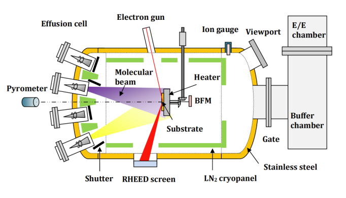
Figure 5. MBE system [12]
3.4.3. Atomic Force Microscopy (AFM). Atomic force microscopy (AFM) can detect the surface topography of semiconductors on the nanometer scale, and compared with scanning electron microscopy, the height and depth characteristics of the sample surface can be effectively measured. The AFM consists of a cantilever, a sample station, a laser source, and a detector [13]. Its working principle is shown in the following figure 6.
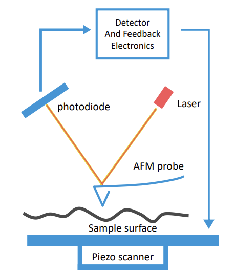
Figure 6. Schematic diagram of atomic force microscopy [13]
3.4.4. X-ray Diffraction (XRD) High resolution. X-ray diffraction (XRD) is the standard tool for the analysis of epitaxial films and is widely used to measure information on material mass, lattice mismatches, strains and superlattice periods, in addition to determining the composition of growing ternary alloys [14]. As shown in the figure 7 below.
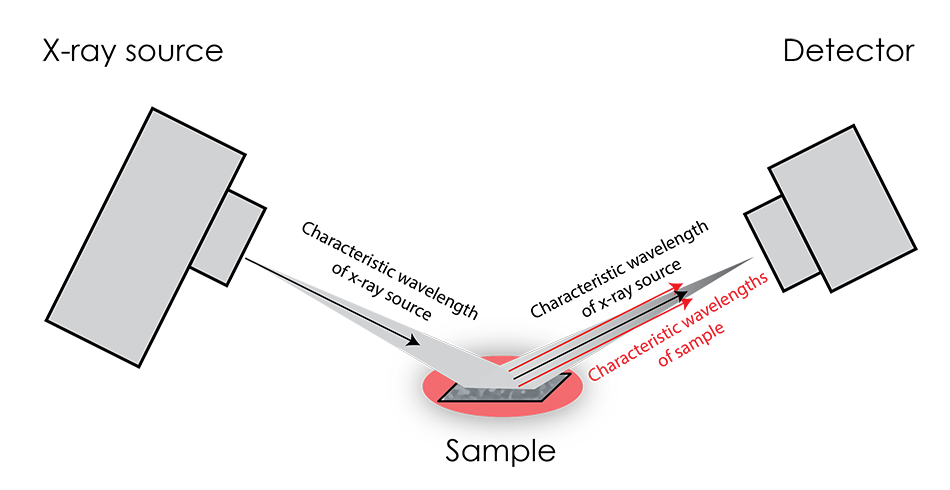
Figure 7. X-ray diffraction (XRD) [14]
4. Future direction of superlattice infrared detectors
The future direction of superlattice infrared detectors may cover several key areas. The research of superlattice materials is an ongoing and challenging field. In the future, the research and development of new materials may continue to drive the performance of superlattice infrared detectors. For example, by exploring new superlattice structures, adding rare earth elements, and changing the preparation process, new materials with superior properties can be found.
Existing superlattice infrared detectors may decline in performance after a long time of use, so improving the stability of their performance is an important direction in the future. This may require further study of the physical and chemical changes in the material over long periods of use and the development of new methods that can maintain the stability of its properties.
The application of quantum well technology in superlattice infrared detectors may further improve their performance. Quantum well technology can control the energy level of electrons, improve the separation efficiency of electrons and holes, and thus improve the response speed and sensitivity of the detector [15].
With the development of microelectronics technology and micro-nano manufacturing technology, superlattice infrared detectors may be further miniaturized and integrated. This will help reduce costs, improve reliability, and potentially provide more effective infrared sensors for future applications such as driverless cars, the Internet of Things, and more.
Future superlattice infrared detectors may have more advanced intelligent functions, such as adaptive regulation, self-diagnosis, self-repair, etc. This will help improve equipment reliability and stability, reduce maintenance costs, and potentially provide better support for unattended and remotely controlled applications.
5. Conclusion
Based on the comprehensive analysis, it’s clear that the field of superlattice infrared detectors is advancing rapidly, driven by innovations in material science and fabrication techniques. The development of InAs/GaInSb Superlattice (SL) infrared detectors, particularly with the introduction of new materials like the Tape InAs/GaSb binary II superlattice, has significantly enhanced the performance capabilities of these detectors. Key advancements include improved signal energy in room and low-temperature environments, enhanced target recognition in complex and low-visibility conditions, and a reduction in dark current and material flaws.
The study’s in-depth examination of temperature optimization and the optimization of stream flux of group V/III elements has led to notable improvements in the quality and efficiency of SL infrared detectors. The selection and optimization of superlattice interfaces have further contributed to the reduction of strain and enhancement of absorption capabilities in infrared detectors.
Looking towards the future, the research highlights several promising directions for superlattice infrared detectors. These include the exploration of new superlattice structures and materials, the application of quantum well technology for improved efficiency, and the integration of advanced microelectronics for miniaturization and cost reduction. Additionally, the potential incorporation of intelligent features like adaptive regulation and self-repair points towards a new era of highly reliable and autonomous infrared detection systems.
References
[1]. Haddadi A, Chen G, Chevallier R, et al. InAs/InAs1− xSbx type-II superlattices for high performance long wavelength infrared detection. Applied Physics Letters, 2014, 105(12).
[2]. Alshahrani D O, Kesaria M, Anyebe E A, et al. Emerging Type‐II Superlattices of InAs/InAsSb and InAs/GaSb for Mid‐Wavelength Infrared Photodetectors. Advanced photonics research, 2022, 3(2): 2100094
[3]. Plis E A. InAs/GaSb type-II superlattice detectors. Advances in Electronics, 2014, 2014.
[4]. Rogalski A, Martyniuk P, Kopytko M. InAs/GaSb type-II superlattice infrared detectors: Future prospect. Applied physics reviews, 2017, 4(3).
[5]. Liu M, You C, Li J, et al. Research on InAs/GaSb type-II superlattice dual-band long-/long-wavelength infrared photodetector. Journal of Infrared and Millimeter Waves, 2023, 42(5): 574-580.
[6]. Zhang J, Chen H, Gu Y, et al. Optimization of growth temperatures for InAlAs metamorphic buffers and high indium InGaAs on InP substrate. Journal of Infrared and Millimeter Waves, 2018, 37(6): 699-703.
[7]. Haugan H J, Grazulis L, Brown G J, et al. Exploring optimum growth for high quality InAs/GaSb type-II superlattices. Journal of crystal growth, 2004, 261(4): 471-478.
[8]. Benyahia D, Michalczewski K, Kębłowski A, et al. Optimization of the interfacial misfit array growth mode of GaSb epilayers on GaAs substrate. Journal of Crystal Growth, 2018, 483: 26-30.
[9]. Machida R, Akahane K, Watanabe I, et al. Advantage of heteroepitaxial GaSb thin-film buffer and GaSb dot nucleation layer for GaSb/AlGaSb multiple quantum well structure grown on Si (1 0 0) substrate by molecular beam epitaxy. Journal of Crystal Growth, 2019, 507: 357-361.
[10]. Li Y, Li X, Hao R, et al. MBE growth of high quality AlInSb/GaSb compound buffer layers on GaAs substrates. Optical and Quantum Electronics, 2020, 52: 1-10.
[11]. Xing F, Ji G, Li Z, et al. Preparation, properties and applications of two-dimensional superlattices. Materials Horizons, 2023, 10(3): 722-744.
[12]. Fastenau J M, Lubyshev D, Qiu Y, et al. MBE growth of GaSb-based photodetectors on 6-inch diameter GaAs substrates via select buffers. Journal of Vacuum Science & Technology B, 2013, 31(3).
[13]. Dazzi A, Prater C B. AFM-IR: Technology and applications in nanoscale infrared spectroscopy and chemical imaging. Chemical reviews, 2017, 117(7): 5146-5173.
[14]. Epp J. X-ray diffraction (XRD) techniques for materials characterization. Materials characterization using nondestructive evaluation (NDE) methods. Woodhead Publishing, 2016: 81-124.
[15]. Rogalski A, Martyniuk P, Kopytko M. InAs/GaSb type-II superlattice infrared detectors: Future prospect. Applied physics reviews, 2017, 4(3).
Cite this article
Li,Z. (2024). Advancements in InAs/GaSb superlattice infrared detectors: Material innovations and optimization techniques. Applied and Computational Engineering,65,97-104.
Data availability
The datasets used and/or analyzed during the current study will be available from the authors upon reasonable request.
Disclaimer/Publisher's Note
The statements, opinions and data contained in all publications are solely those of the individual author(s) and contributor(s) and not of EWA Publishing and/or the editor(s). EWA Publishing and/or the editor(s) disclaim responsibility for any injury to people or property resulting from any ideas, methods, instructions or products referred to in the content.
About volume
Volume title: Proceedings of Urban Intelligence: Machine Learning in Smart City Solutions - CONFSEML 2024
© 2024 by the author(s). Licensee EWA Publishing, Oxford, UK. This article is an open access article distributed under the terms and
conditions of the Creative Commons Attribution (CC BY) license. Authors who
publish this series agree to the following terms:
1. Authors retain copyright and grant the series right of first publication with the work simultaneously licensed under a Creative Commons
Attribution License that allows others to share the work with an acknowledgment of the work's authorship and initial publication in this
series.
2. Authors are able to enter into separate, additional contractual arrangements for the non-exclusive distribution of the series's published
version of the work (e.g., post it to an institutional repository or publish it in a book), with an acknowledgment of its initial
publication in this series.
3. Authors are permitted and encouraged to post their work online (e.g., in institutional repositories or on their website) prior to and
during the submission process, as it can lead to productive exchanges, as well as earlier and greater citation of published work (See
Open access policy for details).
References
[1]. Haddadi A, Chen G, Chevallier R, et al. InAs/InAs1− xSbx type-II superlattices for high performance long wavelength infrared detection. Applied Physics Letters, 2014, 105(12).
[2]. Alshahrani D O, Kesaria M, Anyebe E A, et al. Emerging Type‐II Superlattices of InAs/InAsSb and InAs/GaSb for Mid‐Wavelength Infrared Photodetectors. Advanced photonics research, 2022, 3(2): 2100094
[3]. Plis E A. InAs/GaSb type-II superlattice detectors. Advances in Electronics, 2014, 2014.
[4]. Rogalski A, Martyniuk P, Kopytko M. InAs/GaSb type-II superlattice infrared detectors: Future prospect. Applied physics reviews, 2017, 4(3).
[5]. Liu M, You C, Li J, et al. Research on InAs/GaSb type-II superlattice dual-band long-/long-wavelength infrared photodetector. Journal of Infrared and Millimeter Waves, 2023, 42(5): 574-580.
[6]. Zhang J, Chen H, Gu Y, et al. Optimization of growth temperatures for InAlAs metamorphic buffers and high indium InGaAs on InP substrate. Journal of Infrared and Millimeter Waves, 2018, 37(6): 699-703.
[7]. Haugan H J, Grazulis L, Brown G J, et al. Exploring optimum growth for high quality InAs/GaSb type-II superlattices. Journal of crystal growth, 2004, 261(4): 471-478.
[8]. Benyahia D, Michalczewski K, Kębłowski A, et al. Optimization of the interfacial misfit array growth mode of GaSb epilayers on GaAs substrate. Journal of Crystal Growth, 2018, 483: 26-30.
[9]. Machida R, Akahane K, Watanabe I, et al. Advantage of heteroepitaxial GaSb thin-film buffer and GaSb dot nucleation layer for GaSb/AlGaSb multiple quantum well structure grown on Si (1 0 0) substrate by molecular beam epitaxy. Journal of Crystal Growth, 2019, 507: 357-361.
[10]. Li Y, Li X, Hao R, et al. MBE growth of high quality AlInSb/GaSb compound buffer layers on GaAs substrates. Optical and Quantum Electronics, 2020, 52: 1-10.
[11]. Xing F, Ji G, Li Z, et al. Preparation, properties and applications of two-dimensional superlattices. Materials Horizons, 2023, 10(3): 722-744.
[12]. Fastenau J M, Lubyshev D, Qiu Y, et al. MBE growth of GaSb-based photodetectors on 6-inch diameter GaAs substrates via select buffers. Journal of Vacuum Science & Technology B, 2013, 31(3).
[13]. Dazzi A, Prater C B. AFM-IR: Technology and applications in nanoscale infrared spectroscopy and chemical imaging. Chemical reviews, 2017, 117(7): 5146-5173.
[14]. Epp J. X-ray diffraction (XRD) techniques for materials characterization. Materials characterization using nondestructive evaluation (NDE) methods. Woodhead Publishing, 2016: 81-124.
[15]. Rogalski A, Martyniuk P, Kopytko M. InAs/GaSb type-II superlattice infrared detectors: Future prospect. Applied physics reviews, 2017, 4(3).