


1. Introduction
After Entering the 21st century, the performance of CIS has gradually reached and surpassed that of CCD due to the rapid development of CMOS process technology. In Recent decades, CMOS image sensor (CIS) has gradually replaced CCD and become the mainstream sensor in the market. With the rapid rise of the new energy vehicle industry in recent years, technologies such as Visual recognition and automatic driving (ADAS), auxiliary parking system, fatigue detection and other auxiliary driving technologies for new energy vehicles have also begun to develop synchronously [1]. New energy vehicle manufacturers urgently need an image sensor that meets the vehicle conditions. The characteristics and low cost of CMOS image sensor perfectly meet the technical and market requirements. On-board CMOS image sensors have entered a period of rapid development.
In this paper, the basic theory and characteristics of CMOS transistor are discussed first, and then the structure, characteristics and operation principle of CMOS image sensor using CMOS transistor as an important element are discussed. Three aspects of automatic parking technology, automatic assistant driving technology and fatigue test are discussed.
2. Basic principle of CMOS technology and CMOS image sensor
2.1. Basic theory and structure
Complementary Metal-Oxide-Semiconductor, a term originally describing a specific technology but now broadly applied to a variety of chips manufactured using this process. At its core, a CMOS circuit comprises insulated field-effect transistors. These circuits are unipolar due to the singular type of carrier involved, primarily consisting of an N-channel and a P-channel MOSFET (Metal-Oxide-Semiconductor Field-Effect Transistor). This setup is illustrated in figure 1.
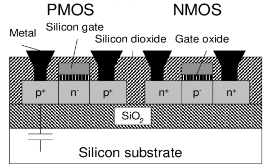
Figure 1. Basic CMOS structure [1]
The operational principle of CMOS technology hinges on the differing polarities of the two gates’ working voltages. By connecting the gates of both transistors as the input and their drains as the output, a complementary working state is achieved where each transistor effectively serves as a load for the other. When the low level (Vin = Vss) is inputted, the PMOS tube is conducted, the Nmos tube is cut off, and the high level is outputted. When the high level (Vin = VDD) is inputted, the PMOS tube is cut off, the Nmos tube is conducted, and the low level is outputted, thereby achieving the effect of an inverter.
2.2. Basic analysis of CMOS image sensor
CMOS image sensor is mainly composed of CMOS image sensor (CIS), which is mainly composed of pixels composed of photosensitive elements, microlenses and microelectronic elements, lead bonds, packages and cover glasses [2]. As shown in figure 2 is an ADC-based image sensor structure.
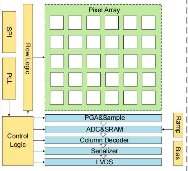
Figure 2. Basic structure of CMOS image sensor [2]
The core of the image sensor is the pixel array, which is composed of photodiodes that can produce photoelectric effect. The principle is that when photons of a certain frequency shine on an object, they will excite electrons to produce current, and the photodiode can store the excited current in the pixel. As shown in the figure 2, when the device starts to work, First, the pixel part will be reset and exposed by Row Logic [3]. After exposure, the whole row will be gated by Row Logic to connect its output to the readout circuit. There will also be a PLL (Phase Locked Loops) in the CMOS imager to generate the on-chip clock; The SPI generates high and low levels to ensure that the control module conforms to the appropriate working mode. The Control Logic is used to generate the periodic timing signals in the chip, which are mainly provided to the Row logic and the readout circuit to ensure that each module works together directly. Bias generation module Bias is used to provide bias current for each analogy module.
2.3. Characteristic
The main advantages of CMOS image sensors are:1. Low power consumption: Compared to CCDs, CMOS requires lower signal bandwidth because each pixel point has a corresponding signal amplifier.2. Cheaper production compared to CCDs: CMOS image sensors are made based on the widely used CMOS technology in the chip field, which has mature technology and a well-established industrial chain.3. On-chip functionality and compatibility with standard CMOS technology: The use of CMOS technology allows devices such as virtual signal processing units and A/D converters to be integrated into the same chip, making it possible for chip-level cameras. This allows the overall size of the camera to be reduced.4. Higher processing speed than CCDs: Unlike CCDs, which can only output programs one by one, CMOS has the ability to randomly output, and the output results can be displayed on a sub-screen. Additionally, due to the multiple digital signal conversion channels, the output speed of CMOS is also faster. However, CMOS also has many drawbacks.
The biggest drawback of CMOS is that noise has a significant impact on image quality. Because the internal components of CMOS are highly integrated and the distance between each component is very small, interference is severe. Therefore, when producing high-density high-quality images, CMOS may not be as good as CCDs [4].
2.4. History of development
In 1963, Morrison published the computable sensor, which became the beginning of. In 1963, Morrison published the computable sensor, which became the beginning of the development of CMOS image sensors. In 1969, Boyle and Smith from Bell Labs successfully invented CCD and proposed its potential applications in imaging. In the 1960s, research on image sensors based on metal oxide semiconductor also began to emerge, but it was not widely used due to immature noise reduction technology at that time. After the 1970s, CCD image sensing technology gradually matured and quickly became the mainstream in the market. In the late 1970s and early 1980s, Hitachi and Matsushita jointly devoted themselves to developing MOS sensors and started to develop portable imaging devices based on this. In 1985, Hitachi proposed the first method of combining CCD and CMOS, which became an important step in the development of CMOS image sensors. In 1995, Fossum invented the active pixel structure of CMOS image sensors and key technologies such as integrated on-chip timing and correlated double sampling, since then, CMOS image sensors have entered a stage of rapid development [5]. Since the 21st century, CMOS image sensors have gradually replaced CCD sensors in the market and become the mainstream in portable photography device sensors.
3. Analysis of CMOS characteristics applied in new energy field
3.1. Parking assistance system
The systems on the market are mainly divided into two types. The first type is based on setting video sensors and CMOS image sensors around the vehicle as shown in Figure 3.
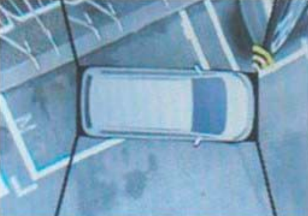
Figure 3. Panoramic visual auxiliary parking system, from Zhao Kai. Research on Panoramic Visualization for Assisted Parking Systems. Hefei University of Technology, 2011.
To obtain the surrounding environment images, which can intuitively display the real-time situation around the vehicle. Drivers can avoid collisions and unnecessary casualties by using this image. The second type, as shown in Figure 4.
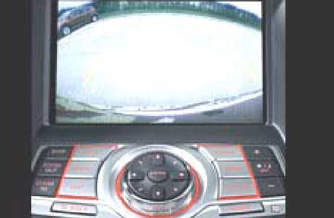
Figure 4. Reversing image monitoring system, from Zhao Kai. Research on Panoramic Visualization for Assisted Parking Systems. Hefei University of Technology, 2011.
It is to set a wide-angle camera at the back of the vehicle to assist drivers in safely parking by providing real-time images of the rear of the vehicle [6]. New energy vehicles mostly use the first type or a combination of both.
On-board image sensors are very demanding. In order to meet these requirements, Zhang Baolong proposed some optimization and processing schemes in his Design of Vehicle High-Definition Panoramic Imaging System Based on CMOS Image Sensor. First of all, for the vehicle electronic system, CIS not only needs to meet the requirements of EMC test and stability, but also needs to meet the requirements of small size and low power consumption. This makes the vehicle-mounted CMOS image sensor have good integration, including photosensitive element array, driving circuit, signal processing circuit, A/D converter and interface circuit. In order to meet the needs of high-definition panoramic imaging, he optimized and processed the selection of crystal oscillator, power supply, chip and passive devices. He chose Si Time’s 24MHz active crystal oscillator with better stability as the clock source for data transmission. To guarantee the power supply’s stability and minimize the impact of electromagnetic interference on the circuit system, he used a double π-type low-pass filter design in the power supply interface. In addition, he also uses a two-stage power supply design, the first stage uses T1’s LMR14203 vehicle-mounted power supply chip, and the second stage uses a 4-channel low dropout linear regulator chip. He also selected LDO chip TLV70033 to supply power to AVDD, TLV70018 to supply power to DS90UB913a, and TPS73615 to supply voltage to DVDD to ensure that the overall power supply system can meet the power consumption requirements of the imaging circuit. In addition to the basic circuit design, he also proposed that the CIS should be placed on the back of the PCB board to keep the traces as short as possible and reduce the interference of power ripple signals on CMOS imaging [7].
3.2. Visual recognition and automatic driving (ADAS)
CMOS image sensor plays an important role in ADAS. Although many ADAS use radar as the main detection means at present, radar detectors for the purpose of pedestrian detection, speed detection, road line detection, traffic signal detection and so on may not be able to detect well. For instance, the low wave reflection of pedestrians makes it difficult for radar to detect accurately [8]. The use of a variety of detection devices paired with each other to make up for the shortcomings is a necessary condition to achieve accurate identification of the driving environment. In order to meet the requirements of ADAS systems, CMOS sensors have different requirements. Isao Takayanagi, Rihito Kuroda, HDR CMOS Image Sensors for Automotive Applications It is mentioned that the sensing range of the sensor is defined between the highest available exposure and the lowest available exposure as shown in the figure 5.
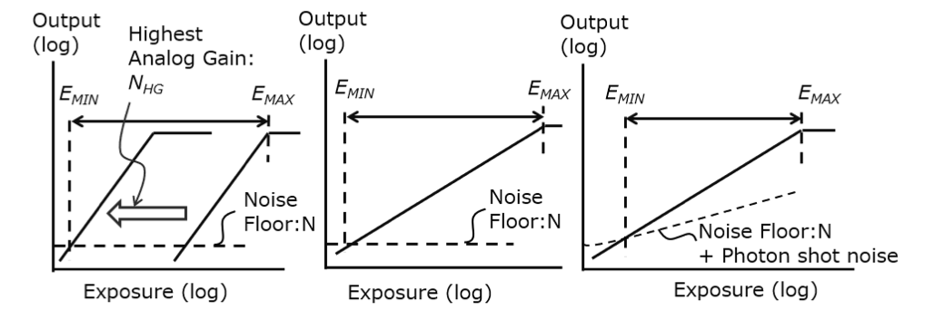
Figure 5. Output curves for different exposures [8]
In this article, unless otherwise specified, the intrascene DR in Fig. 1(b) will be used for discussions. Therefore, max DR is defined as the ratio of the saturation exposure EMAX to the noise equivalent exposure EMIN within an image, as follows:
DR =20 log (Emax/Emin) (1)
Figure 6 shows the scattered intensity of light in a town, expressed in units of CD/m2 as measured from different surfaces. The authors measured about 2000 CD/m2 for an LED traffic light, Pedestrians on the roadside are 1-10 CD/m2 [9]. For this reason, the detector needs a clear boundary to remove background interference and pedestrians. In order to find a suitable boundary, the author introduces the minimum SNR to determine the desired boundary. In general, The SNR of the portrait input is about 4-5. While the surface brightness on the street is about 1 E − RMS or lower.
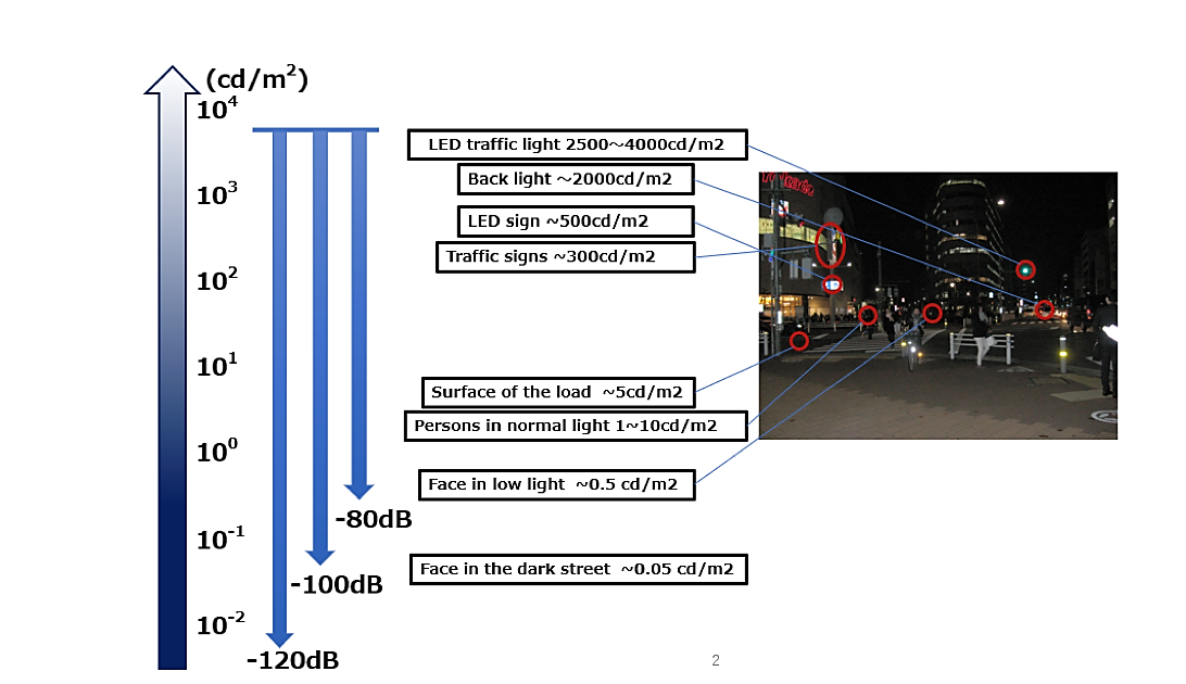
Figure 6. Schematic diagram of the reflection intensity of a small town in a dark environment [9]
In analysing the effects of photon shot noise and dark random noise on the inherent Dynamic Range (DR) of image sensors, an added DR of 24 to 28 dB becomes essential for distinguishing darker objects. Image sensors typically exhibit a base level of dark random noise. However, the application of machine learning for object detection can allow for a reduction in the threshold DR to 20 dB. For instance, as depicted in Figure 6, the minimal DR needed to concurrently identify LED signs and pedestrians on a sidewalk approximates 86 dB (66 dB + 20 dB). Additionally, for scenarios involving both LED traffic lights and individuals in dimly lit streets, the DR requirement is estimated to be around 120 dB.
Moreover, the second author suggests setting the pixel size to 3 micrometers, based on the exposure Emin calculation formula. They also highlight the influence of LED Flicker Mitigation on sensor input quality. A strategy to counter this involves employing sensitive gate control, which divides the integration time into multiple sub-exposures and allocates pulsed sub-exposure durations across the frame period. This approach significantly reduces the likelihood of missing LED pulses.
3.3. Fatigue detection
Machine vision is one of the important technologies of vehicle fatigue detection, which has a wide range of applications. Its process is mainly as follows: first, image acquisition and image preprocessing, then face recognition and feature extraction at the software level, and finally, fatigue assessment and early warning are made by using the extracted values. In addition, the current mainstream imaging images are RGB images and infrared thermal images. The former has a good imaging effect on facial details, facial expressions, eye parts and other facial features, while the latter has a good detection effect on such features as yawning, skin temperature detection and breathing [10]. This paper mainly discusses the image acquisition, such as Xu Xiaopeng in the “Requirements for Image Sensors. Driver Fatigue Detection Method Based on Machine Vision” proposed that when choosing CCD or CMOS as the vehicle sensor, we should use CMOS sensor, because although CCD has better imaging effect at present [11]. However, its high energy consumption and large volume cannot meet the needs of the vehicle. The high integration and low energy consumption of CMOS sensors are fully in line. In addition, the high price of CCD is certainly not in line with the needs of the automotive industry. Among them, I think the high integration of CMOS sensors is an important reason why it is widely used in the automotive field. In the Design of Fatigue Driving Detection System Based on Improved PERCLOS, it is mentioned that the whole fatigue driving detection system is composed of on-board system, cloud server and remote terminal, in which the on-board system is composed of master control, CMOS camera, grip detection circuit and accelerometer. Combined with the above discussion of image requirements, image sensors must be highly integrated to meet the requirements of the vehicle and at the same time maintain good anti-interference ability. To sum up, I think CMOS image sensors with anti-interference, high integration and low cost are the first choice of sensors in fatigue driving technology.
4. Conclusion
This paper describes the practical application of CMOS image sensor in the field of new energy vehicles, aiming to show that CMOS image sensor has a wide range of applications and research significance in the field of new energy vehicles. At present, the new energy automobile industry is in the stage of rapid development, and the new driving technologies brought by it, such as automatic driving, need low-cost CMOS image sensors with better portability and high sensitivity. Therefore, in the next decade, CMOS image sensors will develop in the direction of high integration, high sensitivity, high anti-interference and high durability. At present, CMOS image sensors on the market still have many limitations, such as the high cost and subsequent difficult maintenance problems caused by the selection of high-sensitivity sensors to achieve accurate identification of the surrounding conditions of vehicles, and due to the complex road conditions and environments, low visibility and other environments that interfere with image transmission are often encountered. This is a great challenge for CMOS image sensors which have relatively weak anti-interference ability. To sum up, I think the analysis of CMOS image sensors used in the main vehicle technology in this paper has a certain reference significance for the future development direction of CMOS image sensors.
References
[1]. Jantsch A. CMOS Basics. In: Taking AIMS at Digital Design: Analysis, Improvement, Modeling, and Synthesis. Cham: Springer Nature Switzerland, 2023: 17-44.
[2]. Bigas M, Cabruja E, Forest J, et al. Review of CMOS image sensors. Microelectronics Journal, 2006, 37(5): 433-451.
[3]. Zhang Weisen. Research on Column-Level ADC for CMOS Image Sensors. Dalian University of Technology, 2022.
[4]. El Gamal A, Eltoukhy H. CMOS Image Sensors. IEEE Circuits and Devices Magazine, 2005, 21(3): 6-20.
[5]. Ohta J. Smart CMOS Image Sensors and Applications. CRC Press, 2020.
[6]. Zhao Kai. Research on Panoramic Visualization for Assisted Parking Systems. Hefei University of Technology, 2011.
[7]. Zhang Baolong, Yang Jichao, Li Dan. Design of an Onboard High-Definition Panoramic Imaging System Based on CMOS Image Sensors. Optical Technique, 2015, 41(03): 247-251.
[8]. Zhang Jian. Research on CMOS Low Noise Amplifier Technology for ADAS Systems. University of Electronic Science and Technology of China, 2018.
[9]. Takayanagi I, Kuroda R. HDR CMOS Image Sensors for Automotive Applications. IEEE Transactions on Electron Devices, 2022, 69(6): 2815-2823.
[10]. Yuan Xiang, Sun Xiangmei. Progress in Research on Fatigue Driving Detection Methods. Journal of Automotive Engineering, 2012, 2(03): 157-164.
[11]. Xu Xiaopeng. Research on Driver Fatigue Detection Methods Based on Machine Vision. Jiangsu University of Science and Technology, 2021.
Cite this article
Hu,Y. (2024). Advancements in CMOS image sensors for enhanced vehicle assistance technologies. Applied and Computational Engineering,65,167-173.
Data availability
The datasets used and/or analyzed during the current study will be available from the authors upon reasonable request.
Disclaimer/Publisher's Note
The statements, opinions and data contained in all publications are solely those of the individual author(s) and contributor(s) and not of EWA Publishing and/or the editor(s). EWA Publishing and/or the editor(s) disclaim responsibility for any injury to people or property resulting from any ideas, methods, instructions or products referred to in the content.
About volume
Volume title: Proceedings of Urban Intelligence: Machine Learning in Smart City Solutions - CONFSEML 2024
© 2024 by the author(s). Licensee EWA Publishing, Oxford, UK. This article is an open access article distributed under the terms and
conditions of the Creative Commons Attribution (CC BY) license. Authors who
publish this series agree to the following terms:
1. Authors retain copyright and grant the series right of first publication with the work simultaneously licensed under a Creative Commons
Attribution License that allows others to share the work with an acknowledgment of the work's authorship and initial publication in this
series.
2. Authors are able to enter into separate, additional contractual arrangements for the non-exclusive distribution of the series's published
version of the work (e.g., post it to an institutional repository or publish it in a book), with an acknowledgment of its initial
publication in this series.
3. Authors are permitted and encouraged to post their work online (e.g., in institutional repositories or on their website) prior to and
during the submission process, as it can lead to productive exchanges, as well as earlier and greater citation of published work (See
Open access policy for details).
References
[1]. Jantsch A. CMOS Basics. In: Taking AIMS at Digital Design: Analysis, Improvement, Modeling, and Synthesis. Cham: Springer Nature Switzerland, 2023: 17-44.
[2]. Bigas M, Cabruja E, Forest J, et al. Review of CMOS image sensors. Microelectronics Journal, 2006, 37(5): 433-451.
[3]. Zhang Weisen. Research on Column-Level ADC for CMOS Image Sensors. Dalian University of Technology, 2022.
[4]. El Gamal A, Eltoukhy H. CMOS Image Sensors. IEEE Circuits and Devices Magazine, 2005, 21(3): 6-20.
[5]. Ohta J. Smart CMOS Image Sensors and Applications. CRC Press, 2020.
[6]. Zhao Kai. Research on Panoramic Visualization for Assisted Parking Systems. Hefei University of Technology, 2011.
[7]. Zhang Baolong, Yang Jichao, Li Dan. Design of an Onboard High-Definition Panoramic Imaging System Based on CMOS Image Sensors. Optical Technique, 2015, 41(03): 247-251.
[8]. Zhang Jian. Research on CMOS Low Noise Amplifier Technology for ADAS Systems. University of Electronic Science and Technology of China, 2018.
[9]. Takayanagi I, Kuroda R. HDR CMOS Image Sensors for Automotive Applications. IEEE Transactions on Electron Devices, 2022, 69(6): 2815-2823.
[10]. Yuan Xiang, Sun Xiangmei. Progress in Research on Fatigue Driving Detection Methods. Journal of Automotive Engineering, 2012, 2(03): 157-164.
[11]. Xu Xiaopeng. Research on Driver Fatigue Detection Methods Based on Machine Vision. Jiangsu University of Science and Technology, 2021.