


1. Introduction
The advancement of artificial intelligence calls for efficient hardware for information processing. However, contemporary computers rely on the conventional von Neumann architecture with segregated computing and storage units, resulting in extensive power consumption and time delay during data transfer [1]. Thus, the idea of integrating the computing and storage units i.e., neuromorphic computing, has emerged, which mimics the functionality of the human brain.
While traditional storage technologies such as static random access memory (SRAM), dynamic random access memory (DRAM), and flash have been investigated for neuromorphic computing, the efficient emulation of brain behavior requires the utilization of novel memristive devices. Neuromorphic computing can be physically realized by constructing crossbar arrays with tunable resistance of each cell. The conductance ( \( {G_{ij}} \) ) of each cross-point is used to represent the analog weights observed in biological neural networks. When representing an input vector x through external pulse amplitudes, Ohm's law allows the expression of the current flowing through each device as \( {I_{ij}}={x_{i}}{G_{ij}} \) . Governed by Kirchoff’s law, the total current \( {I_{j}} \) equals to the aggregation of all \( {I_{ij}} \) along a bit line. With multiple columns of memristive devices, the crossbar array enables highly paralleled vector-matrix multiplication (VMM), a key computing primitive in neural networks. Currently, there has been significant research conducted on various categories of memristive devices, including phase change memory (PCM), spin torque transfer memory/spin-orbit torque memory (STT-MRAM/SOT-MRAM), resistive random access memory (ReRAM), ferroelectric random access memory (FeRAM), and electrochemical random access memory (ECRAM) [2].
The memristive characteristics of these devices are greatly influenced by the material properties. Conventional resistive materials include metal oxide materials [3,4], organic materials [5,6], and so on. The recent discovery of two-dimensional transition metal dichalcogenides (TMDCs) has opened up new avenues for device scaling due to their high atomic scale mobility. Furthermore, for some 2D TMDCs, the tunable band structure, ambipolar nature , field-induced phase change, and planar defects make way for unexpected memristive behaviors.
Herein, various switching mechanisms of 2D TMDCs-based memristive devices for neuromorphic computing are discussed, which leads to differences in energy and time consumption, endurance, retention, and memristive behaviors. Besides, the switching characteristics of 2D TMDCs-based memristive devices are also summarized.
2. Switching mechanisms of 2D TMDCs-based memristive devices
TMDCs, an important member of 2D materials, can be represented by the chemical formula \( {MX_{2}} \) . In this formulation, M represents a transition metal atom from group IV–VIII, while X represents a chalcogen atom such as S, Se, or Te. The exceptional optoelectronic characteristics of TMDCs have attracted significant attention from scientists and engineers due to their exceptional optoelectronic characteristics, tunable band gaps, strong spin-orbit coupling effect, and various other physical attributes [7]. Therefore, 2D TMDC-based memristive devices with high performance have been designed for neuromorphic computing applications. Undoubtedly, engineering the memristive devices requires a comprehensive understanding of switching mechanisms. In this section, various switching mechanisms for memristive devices based on 2D TMDCs have been highlighted: (1) floating gate transistor; (2) ferroelectric transistor; (3) formation of conductive filaments; (4) trapping/detrapping of charges; (5) phase transitions; (6) Schottky barrier modulation; (7) electrostatic doping.
2.1. Floating-gate transistor based on 2D TMDCs
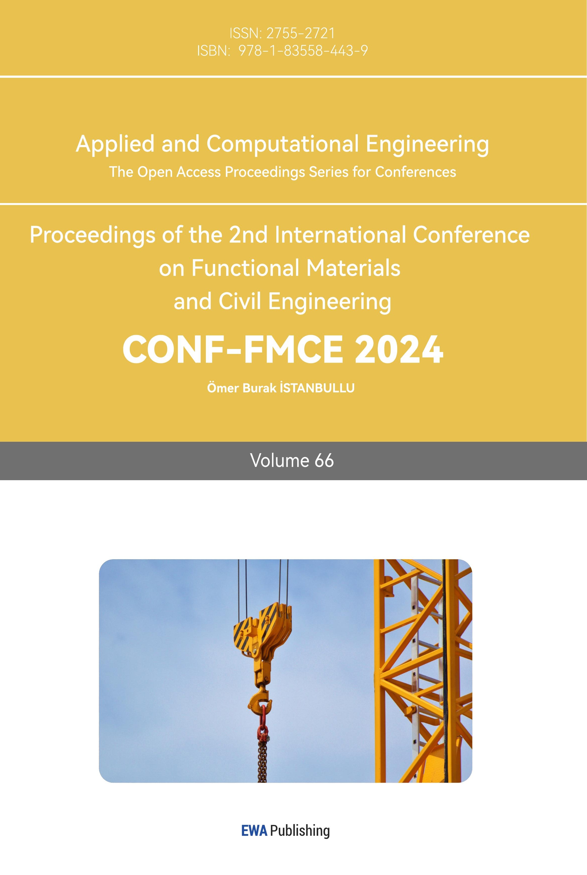
Floating gate field-effect transistors (FGFETs) are extensively utilized for neuromorphic computing. Different from the gate structure of traditional metal oxide semiconductor field-effect transistor (MOSFET), FGFET comprises a control gate and a floating gate, with a thin layer of dielectric in between, thereby forming a capacitor. Electrical charges can be trapped or released from the as-formed capacitor through the tunneling dielectric governed by Fowler-Nordheim tunneling, thereby changing the conductance of the FGFET channel. Semiconducting TMDCs can serve as a channel material for FGFETs scaling due to their high carrier mobility at atomic-scale thickness [8]. Various utilization of TMDCs materials and their van der Waals (vdWs) heterostructures has been observed in enhancing the efficiency of memristive devices. In the study by Park et al. [9], floating-gate transistors were developed using chemical vapor deposition (CVD)-grown \( {MoS_{2}} \) as the channel material (Figure 1(a)). The device exhibited improvements in tunneling efficiency, resulting in non-linearities of approximately 1.9 and 2.2 for potentiation and depression respectively. To optimize electron tunneling and injection processes, Yi et al. [10] introduced a novel memristive device featuring dual floating gates with \( {MoS_{2}} \) serving simultaneously as both the material for the floating gate and the channel (Figure 1(b)). Electron transfers take place not only between the underlying \( {MoS_{2}} \) layer and Au but also between underlying \( {MoS_{2}} \) layer and channel \( {MoS_{2}} \) . In this device, Au works as an extra floating gate, enabling finer control over electron tunneling and injection process. This attribute plays a crucial role in achieving diverse synaptic functionalities.
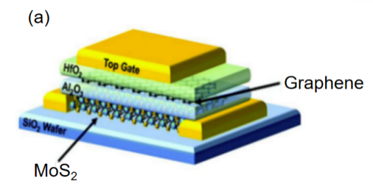
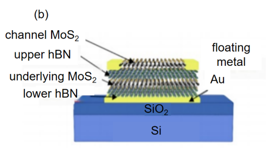
Figure 1. (a) Schematic diagram of floating gate synapse transistor with \( {MoS_{2}} \) and graphene serving as the channel and floating gate, respectively [9] & (b) Schematic diagram of double floating gate structure based on \( {MoS_{2}} \) /h-BN/ \( {MoS_{2}} \) /h-BN/Au stack [10].
2.2. Ferroelectric transistor based on 2D TMDCs
Ferroelectricity is a unique property of specific materials that demonstrate an inherent polarization, capable of being reversed when subjected to an external electric field. Furthermore, Ferroelectrics can be categorized into displacement type ( \( {BaTiO_{3}} \) , \( α{-In_{2}}{Se_{3}} \) , etc.) and ordered-disordered type (Rochelle salt, \( {CuInP_{2}}{S_{6}} \) (CIPS), etc.). By utilizing the properties of polarization reversal and switching effect, ferroelectric field-effect transistors (FeFETs) have been developed for widespread application in neuromorphic computing.
In a FeFET, the ferroelectric layer is used as the gate dielectrics of a FET, where the change of ferroelectric polarization modulates FET channel conductance. After removing the electric field, the polarization state maintains, providing this device with non-volatile properties. Wang et al. [11] reported a nonvolatile FET based on \( {MoS_{2}} \) /h-BN/graphene/CIPS vdWs heterostructure (Figure 2(a)), where \( {MoS_{2}} \) function as the semiconductor channel while CIPS function as the ferroelectric layer. The polarization of the ferroelectric CIPS layer controls the surface potential of \( {MoS_{2}} \) and source-drain current of the underlying 2D FET. Additionally, thanks to the high barrier of h-BN and ideal defect-free surfaces, it becomes feasible to effectively mitigate charge defect capture and leakage, thereby resulting in enhanced stability and electrical performance of transistors. To be more specific, the device exhibits an exceptional on/off ratio( \( {10^{7}} \) ) (Figure 2(b)) as well as a remarkably prolonged data retention time (10 years) (Figure 2(c)).
Recently, it has been demonstrated that the twisted 1T (d1T) phase of TMDCs has become the defined structure of two-dimensional ferroelectricity. In 2014, Shirodkar and Waghmare [12] predicted ferroelectric polarization in monolayer d1T-MoS2 for the first time. In 2023, Jindal et al. [13] found that double-layer \( {Td-MoTe_{2}} \) exhibits both ferroelectric switching and superconductivity. Therefore, 2D TMDCs with ferroelectricity are considered to be promising materials for new-generation nonvolatile memory devices.
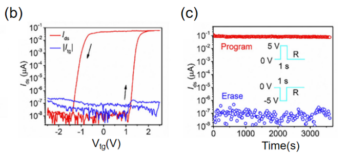
Figure 2. (a) Schematic diagram of an \( {MoS_{2}} \) /h-BN/graphene/CIPS vdW FeFET & (b) Top-gate \( {I_{ds}}-{V_{tg}} \) characteristics (red) and leakage current (black) of a vdWs FeFET & (c) Retention properties of this device at the program and erase states [11].
2.3. Conductive filament formation
By regulating the input voltage pulse or bias sweep, memristive characteristics can be achieved through the formation and control of the conduction filaments. Conductive filament can be divided into metal ion filament and vacancy filament.
Metal ion filament is usually formed by the electrochemical reaction of the active electrode. This mechanism is also called the electrochemical metallization mechanism (ECM). Dielectric layer materials, which are generally solid electrolytes, have high metal ion mobility. At the same time, two electrode materials have different electrochemical activities. When a positive electric field is applied, the active electrode is oxidized and corresponding metal ions are formed. With the continuous redox reaction, more and more metal ions are reduced to a metal state at the cathode and grow to the anode in the form of a metal conductive filament, completing the transition from high resistance to low resistance. When the reverse electric field is applied, the metal conductive filament is fused under the combined action of redox reaction and Joule heat effect, and the memristive device returns to the state of high resistance again. The device exhibits volatile switching behavior, characterized by a low threshold voltage of 0.4V and a high on-off ratio ( \( {10^{6}} \) ). The observed resistive switching phenomenon in this device can be attributed to the formation and self-disruption of Ag conductive filaments through 2D \( {MoS_{2}} \) , as illustrated in Figure 3(c).
Vacancy filament is mainly formed by the original vacancy defects in 2D TMDCs materials and the vacancy accumulation caused by electrical fields. Consequently, according to vacancy distributions, the resistance states of the device may exhibit variations depending on the applied bias. This mechanism is also called the valence transition mechanism (VCM). The oxygen vacancy grows from cathode to anode along the grain boundary, forming a conductive filament connecting two electrodes, and then the transformation from HRS to LRS is completed. When the reverse voltage is applied, the oxygen ions recombine with the oxygen vacancy, leading to the disconnection of the conductive filament and the transformation from LRS to HRS. Compared with ECM, VCM utilizes intrinsic defects to achieve switching characteristics, so it has more reliable switching characteristics. Krishnaprasad et al. [14] designed a memristive device using \( {MoS_{2}} \) / \( {SiO_{x}} \) as an active medium (Figure 3(d)). The vacancy-induced conductive filaments formed by the defects contribute to the trap level in both \( {SiO_{x}} \) and \( {MoS_{2}} \) . Thanks to its underlying mechanism, this memristive device exhibits ideal linearity and symmetry in its conductance update (Figure 3(e)).
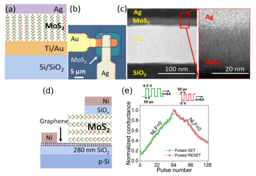
Figure 3. (a) Schematic and (b) optical image of Au/ \( {MoS_{2}} \) /Ag TSM device & (c) STEM and HRTEM image of the cross-section of the vertical stack of \( {MoS_{2}} \) TSM device [15] & (d) Device schematic of graphene/ \( {MoS_{2}} \) / \( {SiO_{x}} \) synapse [14] & (e) Linear and symmetric weight update observed in graphene/ \( {MoS_{2}} \) / \( {SiO_{x}} \) device giving ideal asymmetry of ’0’ [14].
2.4. Charge trapping/detrapping
Due to its stable and reversible physical operation, the charge trapping/detrapping mechanism has been extensively employed in the construction of diverse memristive devices. Space-charge limiting current (SCLC) relies on the capture and release of electrons to modulate the resistance states of memristive devices. Initially, when an external voltage is applied, defects in the dielectric layer will capture electrons injected by the electric field, resulting in a reduced electron density within the dielectric layer and thus exhibiting a high resistance state. Once all defects within the dielectric layer become fully occupied by electrons, the excess electrons become carriers, leading to a rapid increase in current flow and consequently displaying a low resistance state. Krishnaprasad et al. [16] designed a memristive device using \( {MoS_{2}} \) as the switching medium and Ti/Au as the bottom and top electrode (Figure 4(a)). This device exhibits ultra-low cycle-to-cycle (C-C) and device-to-device (D-D) variability in SET voltage and RESET power distributions (Figure 4(b)), showing potential for reliable circuit implementations. This device, with retention of at least 300s for each of the existing 26 states (Figure 4(c)), also exhibits a consistent on/off ratio throughout 1000 DC SET−RESET cycles, indicating its excellent durability. These characteristics of these devices can be attributed to the underlying switching mechanism SCLC. The switching process is facilitated by the trapping and de-trapping phenomena occurring at the interface between \( {MoS_{2}} \) and Ti (top electrode).
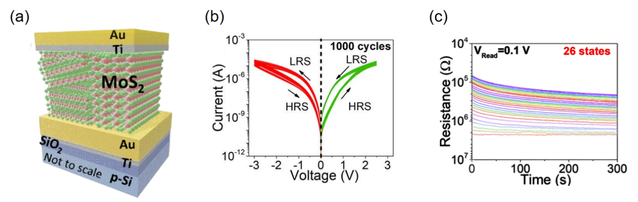
Figure 4. (a) Device schematic & (b) DC cycling: 1000 cycles indicating the low C-C variability and endurance of \( {MoS_{2}} \) devices & (c) Retention of 300s for 26 distinct states [16].
2.5. Phase change
Memristive devices based on phase change possess advantages such as low power consumption, high storage density, and fast response speed. The controllable adjustment of resistance can be realized by utilizing the phase transition properties of TMDCs materials which have multiple stable phases. Zhang et al. [17] reported that electric-field-controlled phase transitions can occur in 2D \( {MoTe_{2}} \) , which can switch between semiconducting (2H) and semimetallic (1T’) phases (Figure 5(a)), resulting in reproducible resistive switching within 10 ns between a high-resistive state (HRS) and a low-resistive state (LRS). Additionally, on/off ratios of \( {10^{6}} \) with programming currents lower than 1 μA were achieved (Figure 5(b)). This study demonstrates the feasibility of controlled electrical state switching in 2D TMDCs and highlights their potential for neuromorphic applications.
By applying strain to bring the material closer to the phase switching point, memristive devices can exhibit enhanced performance. The introduction of strain reduces the energy difference between the semimetallic and semiconducting structural states of the material, thereby requiring a smaller electric field for achieving memristive switching. Hou et al. [18] presented a strain-based 1T’-MoTe2 memristive device in their study (Figure 5(c,d)). Strain-induced and electric-field-induced phase transitions of \( {MoTe_{2}} \) are utilized together, with the former establishing the initial semiconducting active region while the latter enables the reversible resistive switching behavior (Figure 4(e)). This particular device demonstrates low switching voltages of only 90 mV, high on/off ratios ( \( {10^{8}} \) ), fast switching times of 5 ns, and long-term retentions of over \( {10^{5}} \) s, highlighting its significant potential in engineering applications as a strain-based memristive device.
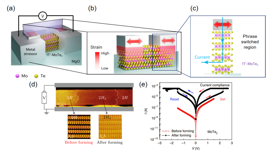
Figure 5. (a) Phase change process of \( {MoTe_{2}} \) with electric field applied and the STEM images of 2H (bottom left) and \( {2H_{d}} \) (bottom right) states of \( {MoTe_{2}} \) & (b) I–V curves of a vertical \( {MoTe_{2}} \) device [17] & (c) Device schematic & (d) Cross section of the device with the strain profile & (e) Mechanism of operation for self-aligned vertical transport based on phase-switched \( {MoTe_{2}} \) directly beneath the contact metal [18].
2.6. Schottky barrier modulation
The Schottky barrier is the rectifying barrier for electrical conduction across heterojunction. It can control the transfer of carriers between the contacted metal and semiconductor. By regulating the electric field to control the motion of defects, the Schottky barrier height and screening length can be modulated, by which channel resistance can be changed. Sangwan et al. [19] have experimentally demonstrated that the bias-induced motion of surfer vacancies in \( {MoS_{2}} \) vary the Schottky barrier heights, thereby tunning the channel resistance of \( {MoS_{2}} \) transistor. By combining the non-volatile feature of surfer vacancies migration and the intrinsic semiconducting behavior of \( {MoS_{2}} \) , the new \( {MoS_{2}} \) transistor can be used as a logic device and memory, thus termed a memtransistor. The two-dimensional \( {MoS_{2}} \) memristive devices (Figure 6(a)) show gate tunability in individual resistance states by four orders of magnitude, accompanied by considerable switching ratios (100), outstanding cycling endurance (500 cycles) and prolonged state retention (over 24 hours). Furthermore, many other factors are found to modulate the height of the Schottky barrier. Lee et al. [20] reported that sulfur vacancy migration assisted by grain boundary of \( {MoS_{2}} \) leads to modulation of the Schottky barrier (Figure 6(b,c)). \( {ZrO_{2-x}} \) induced Schottky barrier modulation [21] and \( {Nb_{2}}{O_{5}} \) induced Schottky barrier modulation [22] are also verified. The oxide insertion layer is essential for efficient modulation of the Schottky barrier, which in turn promotes reliable resistive switching within the \( {MoS_{2}} \) channel and facilitates consistent heterosynaptic plasticity.
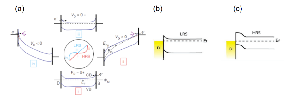
Figure 6. (a) Schematic showing the energy band diagram of an LRS–LRS memtransistor at the four switching stages shown in the centre [19] & (b) Schematic diagram showing a Schottky contact and \( {MoS_{2}} \) band-bending near the drain electrode in LRS. \( {E_{f}} \) is the Fermi energy level [20] & (c) Schematic diagram showing the increased space-charge region near the drain electrode in HRS [20].
2.7. Electrostatic doping of 2D TMDCs
The ultrathin and ambipolar nature of some 2D TMDCs, such as \( {WSe_{2}} \) and \( {WS_{2}} \) , enables switching the material between N or P-type behavior by applying external bias with different polarities efficiently. More specifically, upon external positive/negative bias on the gate, electrons/holes in 2D TMDCs will be attracted and fixed to the gate, thereby allowing only holes/electrons to serve as the majority carrier in the ambipolar TMDCs. Zhou et al. [23] designed a memristive device based on \( {WSe_{2}} \) (Figure 7(a)). By coupling the two gates with opposite voltage pulses ( \( {V_{G1}} \) =- \( {V_{G2}} \) ), different PN and NP junction configurations are realized (Figure 7(b)).
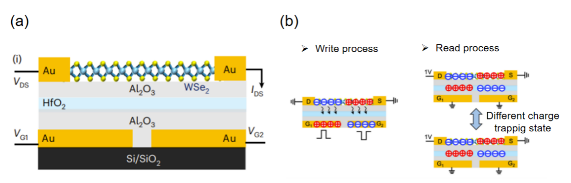

Figure 7. (a) Schematic structure & (b) Schematic of the write and read process of the floating-gate \( {WSe_{2}} \) photodiode [23].
Table 1. Brief summary of switching characteristics of 2D TMDCs based memristive devices.
Structure Switching Mechanism | Mechanism | Switching/ SET voltage(V) | On/Off ratio | Nonlinearity (set) | Nonlinearity (reset) | Endurance (cycles) | Reten-tion | Ref |
Au/hBN/SnS2 | floating gate transistor | / | 2.58×10⁸ | / | / | 15000 | 2.4× 10⁵s | [24] |
HfO2/Graphene/ Al2O3/MoS2 | floating gate transistor | / | 102 | 1.9 | 2.2 | / | 2000s | [9] |
MoS2/h-BN/ Graphene/CIPS | ferroelectric transistor | / | 107 | / | / | 104 | 10 years | [11] |
Cu/MoS2/ AlN/ITO | Cu conductive filament | 4 | 103 | / | / | 1500 | 103s | [25] |
Au/MoS2/Ag | Ag conductive filament | 0.35-0.4 | 106 | / | / | / | / | [14] |
Au/Ti/MoTe2/ Au/Ti | Ag conductive filament | / | 10 | 0.143 | 0.203 | 2000 | 500s | [26] |
Graphene/MoS2/SiOx/Ni | Vacancy conductive filament | 3 | 103 | 0 | 0 | / | 103s | [15] |
Au/Ti/MoS2/ Au/Ti | SCLC | 2.5 | 102 | / | / | 103 | 100s | [16] |
Cu/PVA/ MoS2 QDs/Cu | SCLC | 2 | 150 | / | / | 103 | 104s | [27] |
Ni/Ti/MoTe2 /Au/Ti | Phase change | 2.3 | 106 | / | / | / | 103s | [17] |
1T'-MoTe2 | Phase change | 0.09 | 108 | / | / | 105 | 270s | [18] |
MoS2 | Schottky barrier modulation | 2 | 100 | / | / | 500 | >24h | [19] |
Au/Al2O3/ MoS2 | Schottky barrier modulation | 30 | 103 | / | / | 250 | >24h | [20] |
MoS2/ZrO2-x/ Al2O3 | Schottky barrier modulation | / | 10 | 0.52 | / | 250 | 7000s | [21] |
MoS2/Nb2O5 | Schottky barrier modulation | 8 | 10 | 0.81 | 0.86 | 200 | 1000s | [22] |
WSe2/Al2O3/ HfO2/Al2O3 | Electrostatic doping | 8 | / | / | / | / | 1000s | [23] |
WS2 | Electrostatic doping | / | 106 | 0.63 | 0.1 | 400 | 2000s | [28] |
3. Conclusion
This review systematically summarizes the resistance mechanism and corresponding performances of 2D TMDCs-based memristive devices. These devices show advantages compared with the devices based on conventional materials. In order to achieve large-scale application, there are both challenges and perspectives.
(1) Large-scale preparation of 2D TMDCs is essential for the construction of memristive devices, as the conventional method: exfoliation and CVD both have limitations. Since the industrial scalability and controlled morphology remain challenging, simple and cost-effective synthesis and fabrication methods are still anticipated.
(2) The modification of the existing two-dimensional TMDCs and the control of their properties are prerequisites for designing high-performance 2D TMDCs-based devices for neuromorphic computing. Furthermore, it is imperative to explore and investigate novel switching mechanisms utilizing 2D TMDCs to achieve more reliable switching.
(3) Large-scale integration of memristive devices based on 2D TMDCs with real applications has yet to be shown. Although previous studies have demonstrated a chip consisting of a 32x32 FGFET matrix incorporating up to 1,024 memory devices [29], as well as wafer-level monolithic two-tier 3D integration of \( {MoS_{2}} \) FETs involving over 10,000 devices per tier [30], systematic research effort is still required to further test and improve the functionality of the chip. Recently, advancements in low-heat-budget synthesis techniques enable the direct fabrication of single-layer films without requiring any transfer processes [31], greatly facilitating higher levels of integration density. Therefore, addressing challenges related to material preparation, device fabrication techniques, and innovative device architecture designs is anticipated to pave the way for achieving extensive large-scale integration capabilities in next-generation memristive devices based on 2D TMDCs.
In conclusion, 2D TMDCs show promising potential as candidates for the fabrication of innovative memristive devices, thanks to their abundant semiconductor properties. In the future, the development of application-oriented special neuromorphic computing memristive is still essential. In order to realize this vision, practical steps such as establishing equipment and production lines for synthesizing 2D TMDCs, transferring them onto substrates, evaporating electrodes, and implementing other manufacturing processes are necessary. Additionally, the importance of designing new architectural circuits cannot be overstated.
References
[1]. Mehonic, A. and Kenyon, A.J. (2022). Brain-inspired computing needs a master plan. Nature 604, 255–260.
[2]. Haensch, W., Raghunathan, A., Roy, K., et al. (2022). Compute in-Memory with Non-Volatile Elements for Neural Networks: A Review from a Co-Design Perspective. https://webofscience.clarivate.cn/wos/alldb/full-record/WOS:000942630400001
[3]. Lee, J.H., Park, S.P., Park, K. and Kim, H.J. (2019). Flexible and waterproof resistive random-access memory based on nitrocellulose for skin-attachable wearable devices. Adv Funct Mater, 30, 190743.
[4]. Li, W., Guo, F., Ling, H., et al. (2018). Solution-processed wide-bandgap organic semiconductor nanostructures arrays for nonvolatile organic field-effect transistor memory. Small, 14, 17014.
[5]. Chang, T., Jo, S.H. and Lu, W. (2011). Short-term memory to long-term memory transition in a nanoscale memristor. ACS nano, 5(9), 7669-7676.
[6]. Qin, G., Huang, A.P., Hu, Q., et al. (2019). Stability and Repeatability of a Karst-like Hierarchical Porous Silicon Oxide-Based Memristor. ACS Applied Materials & Interfaces, 11(24), 21734-21740.
[7]. Zhao, B., Shen, D.Y., Zhang, Z.C., et al. (2021). 2D Metallic Transition-Metal Dichalcogenides: Structures, Synthesis, Properties, and Applications. Adv. Funct. Mater., 2105132.
[8]. Manzeli, S., Ovchinnikov, D., Pasquier, D., et al. (2017). 2D transition metal dichalcogenides. Nat Rev Mater 2, 17033.
[9]. Park, M., Kim, T.S., Kim, I.S., et al. (2020). A 2D material-based floating gate device with linear synaptic weight update. Nanoscale, 12(48), 24503-24509.
[10]. Yi, S.G., Park, M.U., Kim, S.H., et al. (2018). Artificial Synaptic Emulators Based on MoS2 Flash Memory Devices with Double Floating Gates. ACS Applied Materials and Interfaces, 10(37), 31480-31487.
[11]. Wang, X., Zhu, C., Deng, Y., et al. (2021). Van der Waals engineering of ferroelectric heterostructures for long-retention memory. Nat Commun, 12, 1109.
[12]. Shirodkar, S.N. and Waghmare, U.V. (2014). Emergence of ferroelectricity at a metal-semiconductor transition in a T1 monolayer of MoS2. Phys Rev Lett, 112, 157601.
[13]. Jindal, A., Saha, A., Li, Z., et al. (2023). Coupled ferroelectricity and superconductivity in bilayer Td-MoTe2. Nature, 613, 48-52.
[14]. Krishnaprasad, A., Dev, D., Shawkat, M.S., et al. (2023). Graphene/MoS2/SiOx memristive synapses for linear weight update. npj 2D Mater Appl, 7, 22.
[15]. Dev, D., Krishnaprasad, A., Shawkat, M.S., et al. (2020). 2DMoS2-based threshold switching memristor for artificial neuron. IEEE Electron Device Lett., 41(6), 936–939.
[16]. Krishnaprasad, A., Dev, D., Han, S.S., et al. (2022). MoS2 Synapses with Ultra-low Variability and Their Implementation in Boolean Logic. ACS nano, 16(2), 2866–2876.
[17]. Zhang, F., Zhang, H., Krylyuk, S., et al. (2019). Electric-field induced structural transition in vertical MoTe2- and Mo1–xWxTe2-based resistive memories. Nature Mater, 18, 55–61.
[18]. Hou, W., Azizimanesh, A., Dey, A., et al. (2023). Strain engineering of vertical molybdenum ditelluride phase-change memristors. Nature Electronics.
[19]. Sangwan, V.K., Lee, H., Bergeron, H., et al. (2018). Multi-terminal memtransistors from polycrystalline monolayer molybdenum disulfide. Nature, 554(7693), 500-504,504A-504M.
[20]. Lee, H.S., Sangwan, V.K., Gaviria Rojas, W.A., et al. (2020). Dual‐Gated MoS2 Memtransistor Crossbar Array. Advanced Functional Materials. https://doi.org/10.1002/adfm.202003683.
[21]. Jang, H.Y., Kwon, O., Nam, J.H., et al. (2022). Highly Reproducible Heterosynaptic Plasticity Enabled by MoS2/ZrO2-x Heterostructure Memtransistor. ACS applied materials & interfaces, 14(46), 52173–52181.
[22]. Nam, J.H., Oh, S., Jang, H.Y., et al. (2021). Low Power MoS2/Nb2O5 Memtransistor Device with Highly Reliable Heterosynaptic Plasticity (Adv. Funct. Mater. 40/2021). Advanced Functional Materials.
[23]. Zhou, Y., Fu, J., Chen, Z., et al. (2023). Computational event-driven vision sensors for in-sensor spiking neural networks. Nat Electron, 6, 870–878.
[24]. Khan, M.A., Yim, S., Rehman, S., et al. (2023). Two-dimensional materials memory devices with floating metal gate for neuromorphic applications. Materials Today Advances, 20, 100438.
[25]. Sharma, S., Kumar, A., Dutta, S., et al. (2020). Optically triggered multilevel resistive switching characteristics of Cu/MoS2/AlN/ITO bilayer memory structure. Applied Physics Letters, 117, 192101.
[26]. He, H., Rui, Y., Jian, X., et al. (2022). High-uniformity Memristor Arrays Based on Two-dimensional MoTe2 for Neuromorphic Computing. Journal of Inorganic Materials, 37(7), 795-801.
[27]. Koduvayur Ganeshan, S., Selamneni, V. and Sahatiya, P. (2020). Water dissolvable MoS2 quantum dots/PVA film as an active material for destructible memristors. New Journal of Chemistry, 44, 11941-11948.
[28]. Mallik, S.K., Padhan, R., Sahu, M.C., et al. (2023). Ionotronic WS2 memtransistors for 6-bit storage and neuromorphic adaptation at high temperature. npj 2D Mater Appl, 7, 63.
[29]. Migliato Marega, G., Ji, H.G., Wang, Z., et al. (2023). A large-scale integrated vector–matrix multiplication processor based on monolayer molybdenum disulfide memories. Nat Electron, 6, 991–998.
[30]. Jayachandran, D., Pendurthi, R., Sadaf, M.U.K., et al. (2024). Three-dimensional integration of two-dimensional field-effect transistors. Nature, 625, 276–281.
[31]. Zhu, J., Park, J.H., Vitale, S.A., et al. (2023). Low-thermal-budget synthesis of monolayer molybdenum disulfide for silicon back-end-of-line integration on a 200 mm platform. Nat. Nanotechnol., 18, 456–463.
Cite this article
Wang,Y. (2024). Switching mechanisms of two-dimensional transition metal dichalcogenides(2D TMDCs)-based memristive devices for neuromorphic computing. Applied and Computational Engineering,66,61-70.
Data availability
The datasets used and/or analyzed during the current study will be available from the authors upon reasonable request.
Disclaimer/Publisher's Note
The statements, opinions and data contained in all publications are solely those of the individual author(s) and contributor(s) and not of EWA Publishing and/or the editor(s). EWA Publishing and/or the editor(s) disclaim responsibility for any injury to people or property resulting from any ideas, methods, instructions or products referred to in the content.
About volume
Volume title: Proceedings of the 2nd International Conference on Functional Materials and Civil Engineering
© 2024 by the author(s). Licensee EWA Publishing, Oxford, UK. This article is an open access article distributed under the terms and
conditions of the Creative Commons Attribution (CC BY) license. Authors who
publish this series agree to the following terms:
1. Authors retain copyright and grant the series right of first publication with the work simultaneously licensed under a Creative Commons
Attribution License that allows others to share the work with an acknowledgment of the work's authorship and initial publication in this
series.
2. Authors are able to enter into separate, additional contractual arrangements for the non-exclusive distribution of the series's published
version of the work (e.g., post it to an institutional repository or publish it in a book), with an acknowledgment of its initial
publication in this series.
3. Authors are permitted and encouraged to post their work online (e.g., in institutional repositories or on their website) prior to and
during the submission process, as it can lead to productive exchanges, as well as earlier and greater citation of published work (See
Open access policy for details).
References
[1]. Mehonic, A. and Kenyon, A.J. (2022). Brain-inspired computing needs a master plan. Nature 604, 255–260.
[2]. Haensch, W., Raghunathan, A., Roy, K., et al. (2022). Compute in-Memory with Non-Volatile Elements for Neural Networks: A Review from a Co-Design Perspective. https://webofscience.clarivate.cn/wos/alldb/full-record/WOS:000942630400001
[3]. Lee, J.H., Park, S.P., Park, K. and Kim, H.J. (2019). Flexible and waterproof resistive random-access memory based on nitrocellulose for skin-attachable wearable devices. Adv Funct Mater, 30, 190743.
[4]. Li, W., Guo, F., Ling, H., et al. (2018). Solution-processed wide-bandgap organic semiconductor nanostructures arrays for nonvolatile organic field-effect transistor memory. Small, 14, 17014.
[5]. Chang, T., Jo, S.H. and Lu, W. (2011). Short-term memory to long-term memory transition in a nanoscale memristor. ACS nano, 5(9), 7669-7676.
[6]. Qin, G., Huang, A.P., Hu, Q., et al. (2019). Stability and Repeatability of a Karst-like Hierarchical Porous Silicon Oxide-Based Memristor. ACS Applied Materials & Interfaces, 11(24), 21734-21740.
[7]. Zhao, B., Shen, D.Y., Zhang, Z.C., et al. (2021). 2D Metallic Transition-Metal Dichalcogenides: Structures, Synthesis, Properties, and Applications. Adv. Funct. Mater., 2105132.
[8]. Manzeli, S., Ovchinnikov, D., Pasquier, D., et al. (2017). 2D transition metal dichalcogenides. Nat Rev Mater 2, 17033.
[9]. Park, M., Kim, T.S., Kim, I.S., et al. (2020). A 2D material-based floating gate device with linear synaptic weight update. Nanoscale, 12(48), 24503-24509.
[10]. Yi, S.G., Park, M.U., Kim, S.H., et al. (2018). Artificial Synaptic Emulators Based on MoS2 Flash Memory Devices with Double Floating Gates. ACS Applied Materials and Interfaces, 10(37), 31480-31487.
[11]. Wang, X., Zhu, C., Deng, Y., et al. (2021). Van der Waals engineering of ferroelectric heterostructures for long-retention memory. Nat Commun, 12, 1109.
[12]. Shirodkar, S.N. and Waghmare, U.V. (2014). Emergence of ferroelectricity at a metal-semiconductor transition in a T1 monolayer of MoS2. Phys Rev Lett, 112, 157601.
[13]. Jindal, A., Saha, A., Li, Z., et al. (2023). Coupled ferroelectricity and superconductivity in bilayer Td-MoTe2. Nature, 613, 48-52.
[14]. Krishnaprasad, A., Dev, D., Shawkat, M.S., et al. (2023). Graphene/MoS2/SiOx memristive synapses for linear weight update. npj 2D Mater Appl, 7, 22.
[15]. Dev, D., Krishnaprasad, A., Shawkat, M.S., et al. (2020). 2DMoS2-based threshold switching memristor for artificial neuron. IEEE Electron Device Lett., 41(6), 936–939.
[16]. Krishnaprasad, A., Dev, D., Han, S.S., et al. (2022). MoS2 Synapses with Ultra-low Variability and Their Implementation in Boolean Logic. ACS nano, 16(2), 2866–2876.
[17]. Zhang, F., Zhang, H., Krylyuk, S., et al. (2019). Electric-field induced structural transition in vertical MoTe2- and Mo1–xWxTe2-based resistive memories. Nature Mater, 18, 55–61.
[18]. Hou, W., Azizimanesh, A., Dey, A., et al. (2023). Strain engineering of vertical molybdenum ditelluride phase-change memristors. Nature Electronics.
[19]. Sangwan, V.K., Lee, H., Bergeron, H., et al. (2018). Multi-terminal memtransistors from polycrystalline monolayer molybdenum disulfide. Nature, 554(7693), 500-504,504A-504M.
[20]. Lee, H.S., Sangwan, V.K., Gaviria Rojas, W.A., et al. (2020). Dual‐Gated MoS2 Memtransistor Crossbar Array. Advanced Functional Materials. https://doi.org/10.1002/adfm.202003683.
[21]. Jang, H.Y., Kwon, O., Nam, J.H., et al. (2022). Highly Reproducible Heterosynaptic Plasticity Enabled by MoS2/ZrO2-x Heterostructure Memtransistor. ACS applied materials & interfaces, 14(46), 52173–52181.
[22]. Nam, J.H., Oh, S., Jang, H.Y., et al. (2021). Low Power MoS2/Nb2O5 Memtransistor Device with Highly Reliable Heterosynaptic Plasticity (Adv. Funct. Mater. 40/2021). Advanced Functional Materials.
[23]. Zhou, Y., Fu, J., Chen, Z., et al. (2023). Computational event-driven vision sensors for in-sensor spiking neural networks. Nat Electron, 6, 870–878.
[24]. Khan, M.A., Yim, S., Rehman, S., et al. (2023). Two-dimensional materials memory devices with floating metal gate for neuromorphic applications. Materials Today Advances, 20, 100438.
[25]. Sharma, S., Kumar, A., Dutta, S., et al. (2020). Optically triggered multilevel resistive switching characteristics of Cu/MoS2/AlN/ITO bilayer memory structure. Applied Physics Letters, 117, 192101.
[26]. He, H., Rui, Y., Jian, X., et al. (2022). High-uniformity Memristor Arrays Based on Two-dimensional MoTe2 for Neuromorphic Computing. Journal of Inorganic Materials, 37(7), 795-801.
[27]. Koduvayur Ganeshan, S., Selamneni, V. and Sahatiya, P. (2020). Water dissolvable MoS2 quantum dots/PVA film as an active material for destructible memristors. New Journal of Chemistry, 44, 11941-11948.
[28]. Mallik, S.K., Padhan, R., Sahu, M.C., et al. (2023). Ionotronic WS2 memtransistors for 6-bit storage and neuromorphic adaptation at high temperature. npj 2D Mater Appl, 7, 63.
[29]. Migliato Marega, G., Ji, H.G., Wang, Z., et al. (2023). A large-scale integrated vector–matrix multiplication processor based on monolayer molybdenum disulfide memories. Nat Electron, 6, 991–998.
[30]. Jayachandran, D., Pendurthi, R., Sadaf, M.U.K., et al. (2024). Three-dimensional integration of two-dimensional field-effect transistors. Nature, 625, 276–281.
[31]. Zhu, J., Park, J.H., Vitale, S.A., et al. (2023). Low-thermal-budget synthesis of monolayer molybdenum disulfide for silicon back-end-of-line integration on a 200 mm platform. Nat. Nanotechnol., 18, 456–463.