


1. Introduction
Previous scholars have primarily focused on specific aspects when exploring and systematically summarizing the research on integrated circuits. For example, the upstream industry of integrated circuits [1] improve the conductivity of the wafer so as to enhance chip performances in the subsequent manufacturing processes [2]. In the midstream of the integrated circuit industry, due to its complexity, scientists often tend to focus on studying specific processes within the manufacturing chain, such as the physical mechanisms behind photolithography, etching, doping and deposition. Scholars aim to improve and innovate these processes to achieve cost reduction, enhance production stability, or improve chip performances. In the downstream of the industry, the packaging and testing stages have also attracted many scholars to conduct specialized researches in this area. The research outcomes typically focus on improving the standardization [3] of integrated circuit testing or designing new diverse packaging [4] and testing methods to enhance testing accuracy.
However, this paper emphasizes the rapid and systematic representation of the current global development process of integrated circuits. With the growing habit of fragmented reading, specialized researches in a specific direction may not be conducive to readers who are encountering the integrated circuit industry for the first time, but have certain demands and hope to quickly gain a general understanding of the technologies used in the industry and the domestic and international status of the industry. To enable more people to understand how a chip in smartphones, computers, or other electronic products is made, a systematic and comprehensive overview of integrated circuit technology and the industry is organized in this manuscript.
2. The basic semiconductor materials: wafer
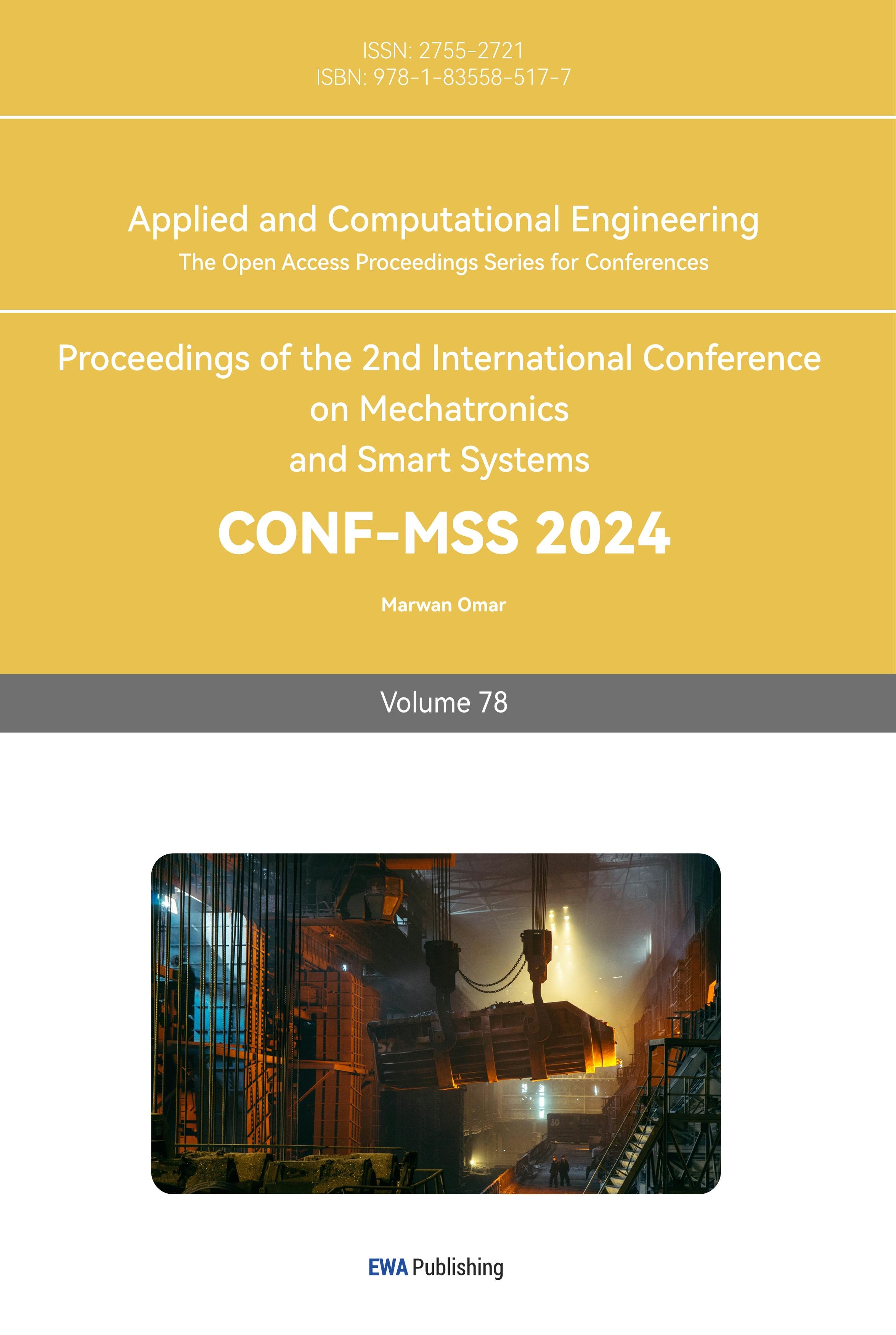
Wafer is a thin cylindrical material to make a chip, and generally made of silicon as shown in figure 1, which takes up the most part of global semiconductor market. In addition, nowadays there are also some wafer made by new materials, such as SiC [5], GaN [6], GaAs [7], GaO [8], AlN [9] and some two-dimensional materials [9, 10].
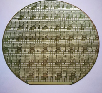
Figure 1. A wafer of Chinese-manufactured silicon carbide MOSFET [1].
So far, wafer is the most important material to make semiconductor devices and build integrated circuits. Due to its different physical and chemical properties, the silicon wafers can be sorted into different applications. For example, 8 inches and 12 inches silicon wafers are widely used in advanced logic circuits, power devices and storage chips. While smaller wafers with size up to 6 inches are usually used to make discrete devices. Generally, the bigger a wafer is, the more chips it can carry, which will effectively reduce the production and manufacturing costs of individual chips. Wafers can also be sorted by the doping degree, manufacturing processes or their application scenarios.
When we come to the fabrication of a wafer, there are plenty of complex technologies. Among which, most of them are focused on modifying the performance of a wafer, eliminating the unwanted injury on the wafer surface, cleaning the dirt or particles. The main processes will be introduced in the next paragraph.
The first process will be the Czochralsk and Float-Zone method to change polycrystalline silicon into monocrystalline silicon and to form the silicon ingot. The monocrystalline silicon produced by these two methods is slightly different in performances, and monocrystalline sillcon produced by Czochralsk is more widely used due to its lower price. The second process is slicing. Using wire saw machines, the silicon ingot can be sliced into thin cylindrical pieces. After this, beveling, grinding, etching and polishing processes will also be needed to make the surface of sliced pieces more smooth and thinner. After further cleaning and particle checking, the qualified silicon wafer can be packed and sold to customers for chip production.
China’s semiconductor industries still have some barriers to overcome. For instance, the surface cleanness, the evenness and the crystal defects are strictly restricted, due to which some time are still needed to improve our technology in silicon industry. Commercially, some time is also needed for a new wafer supplier to be recognized by the market, to make sure the product are qualified and stable. A wafer-producing factory is usually too expensive to private capitals, so only government capitals have the willingness to build factories to manufacture wafers and address social employment issues. Last but not least, the number of professionals is too small because China relied too much on international suppliers in the past decades, which makes the local technology development more difficult.
3. The main fabrication processes
The first transistor in the world was created in 1949 by three American scientist, who started a new century of applying semiconductor. Then in 1958, a young engineer named Jack Kilby built the first piece of integrated circuit in human history and began the large-scale application of integrated circuits (IC). Over the following few decades, integrated circuits and semiconductor industry have become one of the most prosperous industries around the world. The applications of IC are not only in electronics, but also inaviation, telecommunication, and military. In modern world, due to the limitation of technology and economic factors, the growth rate of IC industry cannot maintain as fast as that in the last century, but still keeps an upward trend.
In the initial stage, America was the dominant country for integrated circuit manufacturing. Then in the 1980s, Japanese tried to challenge the leading role of American, but finally failed [11].Considering the biggest market of IC in China, the Chinese government is trying to promote the developing of IC industry, but because of the high cost and the lacking of professionals, Chinese national IC industry still has a long way to go.
For nowadays technology of producing integrated circuits, photolithography maintains its position of the most complex, expensive and important process in semiconductor manufacturing [12]. Photolithography in integrated circuits is a technique to precisely copy the pattern from photo masks to the wafer substrates, as shown in figure 2. A gluing process is the start of a photolithography [13]. The composition of the photoresist will directly affect the photolithography effects. Rotary gluing is the most commonly used gluing method to make sure thin film forming above the wafers [14]. Then it comes to the most important process in the lithography ⸺ the exposure . Exposure uses the light giving out by the light source and a series of prism to print patterns on the wafer covered by photoresist [13, 15, 16]. After exposure, the polymer formed by the previous gluing step is removed by the development process. Then the pattern generated by the exposure step can be observed by microscopes.
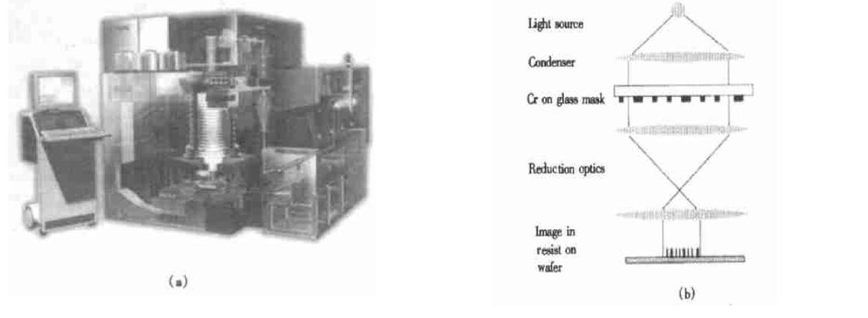
Figure 2. The structural diagram of a certain company’s photolithography machine [2]. (a) A commercial lithography machine; (b) A schematic diagram of exposure system.
If we need to form a thin film on the wafer to isolate different devices and connecting lines, an oxidation process will be needed. The film is usually made of silicon dioxide and silicon nitride, which is not only the excellent insulating material, but also easily to form. And the etching process will remove those unwanted films on the wafer surface by using hydrofluoric acid, or by physical peeling [17]. Doping is an operation that changes the electrical conductivity by mixing other impurities into a substrate material. The ion implantation and physical diffusion are two common ways to inject impurity ions into wafers.
4. The package and test process
After fabrication processes in the fab, wafers will be packaged and tested to assess whether the manufactured chips meet the required standards.
Figure 3. Embedded packaging example(3)
Semiconductor package is a technique that enclosing a designed integrated circuits (IC) in order to protect its circuits and devices, which is in a protecting casing made of a certain material such as mental, plastic or ceramic, as shown in figure 3. The purpose is not only providing protection against damage or contamination to the internal structure of the IC, but also connecting the internal components with external chips.
Nowadays, fabless mode is used by most of the companies that are running the service of packaging semiconductors, except Intel and Samsung. Fabless companies do not package and test IC functions by themselves, but handing over the work to specialized companies for packaging and testing processes.
The packaging of semiconductors can vary depending on specific details. Different packaging techniques can be selected based on different packaging requirements, such as the packaging material (metal, ceramic, or plastic), the packaging molding process (pre-mold or postmold), and the external shape of the packaged product (SIP, DIP, PLCC, PQFP, SOP, TSOP, PPGA, PBGA, CSP) [18]. Nowadays, with the development of craft of the packaging, semiconductors can also be packaged using the technique of Flip-Chip or SIP. The former focuses on optimizing the semiconductor’s reception performance for high-frequency signals and compressing the integration space of the semiconductor to achieve more efficient utilization of space. The latter, on the other hand, emphasizes the number of functions that can be achieved on a per-unit area of the semiconductor. In other words, for chips of the same size, individual units packaged using SIP technology can achieve more functionalities.
Semiconductor testing refers to the testing of packaged IC for their basic functionality parameters, including both wafer-level testing (CP) and final product testing (FT). Only the products that pass the tests and meet the requirements can be delivered to customers as commodities.
Compared with other parts in the integrated circuit industry chain, the development of semiconductor packaging and testing of China has been relatively more competitive, and occupied a certain share in the international industry chain segments. However, most of the packaging or testing companies in mainland China are still faced with the problem that the packaging techniques are not advanced enough. Only relatively simple functions can be achieved compared to international leading companies like Taiwan’s TSMC, and the profits gained by these companies are relatively low. But with the gradual withdrawal of companies of other areas such as Japan, South Korea, and the United States in this business field, semiconductor packaging and testing enterprises in mainland China still have immeasurable development space [19].
5. Conclusion
Integrated circuits, as a widely applied technology in human society, should be as familiar to people as literature, mathematics, or language. It is not only important for individuals to have a basic understanding of the production methods and current state of the tools they are currently using and will use more frequently in the future, but also serves as a powerful driving force for the advancement of the integrated circuit industry and human civilization as a whole. The overview may not be perfect and extremely detailed. Further efforts and research are still needed to promote and make this technology known to everyone.
References
[1]. Y. Wang and J. Kang, “Development and Challenges of Lithography for ULSI,” Journal of Semiconductors, no. 03, pp. 225-237, 2002.
[2]. C. Jun, “Summary of Silicon Carbide Semiconductor Technology and Market Application,” Application of IC, vol. 35, no. 08, pp. 5-9, 2018.
[3]. X. Kong and Q. Li, “Overview of Research in IC testing and Standardization Field,” Information Technology & Standardization, no. 07, pp. 39-43, 2023.
[4]. Y. Z. Fanwen Yang, “Situation and Development of Epoxy Resins for Electronic Packaging,” Electronics Process Technology, no. 06, pp. 238-241, 2001.
[5]. Z. H. Ni, W. Chen, X. F. Fan, J. L. Kuo, and Z. X. Shen, “Raman Spectroscopy of Epitaxial Graphene on a SiC Substrate,” Physical Review B, vol. 77, no. 11, 2008.
[6]. T. Miyoshi et al., “510–515 nm InGaN-Based Green Laser Diodes on c-Plane GaN Substrate,” Applied Physics Express, vol. 2, no. 6, pp. 062201-062201-3, 2009.
[7]. D. Hyman, J. Lam, B. Warneke, A. Schmitz, and J. Lee, “Surface-micromachined RF MEMS switches on GaAs substrate,” International Journal of RF and Microwave Computer-Aided Engineering, vol. 9, no. 4, pp. 348-361, 2015.
[8]. G. B. Gao and H. H. Hoang, “Method for forming a CMOS circuit of GaAS/Ge on Si substrate,” 2003.
[9]. J. W. Lee and I. R. Alexe, “Oxidation behavior of AlN substrate at low temperature,” Journal of Materials Science: Materials in Electronics, 2002.
[10]. J. Huang and J. E. Goldberger, “Two-dimensional materials,” Journal of Solid State Chemistry, vol. 224, pp. 1-1, 2015.
[11]. L. Wang, “The Past, Present, and Future of Integrated Circuits (Part 1) - The Development History of Integrated Circuits in the World,” Application of IC, no. 01, pp. 36-40, 2014.
[12]. B. Wu and A. Kumar, “Extreme ultraviolet lithography: A review,” Journal of Vacuum Science & Technology B Microelectronics & Nanometer Structures, vol. 25, no. 6, pp. 1743-1761, 2007.
[13]. Wood and R. O., “Wavelength dependence of the resist sidewall angle in extreme ultraviolet lithography,” Journal of Vacuum Science & Technology B, vol. 12, no. 6, pp. 3841-3845, 1994.
[14]. D. Xiang, M. He, D. Qu, P. Mou, and G. Duan, “Development of Coating of Photoresist in Semiconductor Manufacturing,” China Mechanical Engineering, vol. 23, no. 03, pp. 354-361, 2012.
[15]. H. Wang and J. Zhu, “The discuss of exposure technology in lithography process,” Modern Manufacturing Engineering, no. 12, pp. 131-135, 2008.
[16]. J. S. Kim and J. Ahn, “Mask Materials and Designs for Extreme Ultra Violet Lithography,” Electronic Materials Letters, 2018.
[17]. J. Yan, K. Yuan, H. Tai, and Z. Wu, “Research of the Etching Process for Silicon Dioxide,” Microprocessors, vol. 31, no. 02, pp. 16-18+22, 2010.
[18]. W. Mei, “Semiconductor Package Introduction,” Equipment for Electronic Products Manufacturing, no. 05, pp. 14-21, 2005.
[19]. Z. Zhou, “The Future Technology Trends of Integrated Circuit Packaging and Testing Industry and Its Development in China,” Electronics & Packaging, vol. 15, no. 01, pp. 1-5, 2015.
Cite this article
Lei,W.;Yao,S. (2024). A basic introduction to integrated circuit technology . Applied and Computational Engineering,78,54-59.
Data availability
The datasets used and/or analyzed during the current study will be available from the authors upon reasonable request.
Disclaimer/Publisher's Note
The statements, opinions and data contained in all publications are solely those of the individual author(s) and contributor(s) and not of EWA Publishing and/or the editor(s). EWA Publishing and/or the editor(s) disclaim responsibility for any injury to people or property resulting from any ideas, methods, instructions or products referred to in the content.
About volume
Volume title: Proceedings of the 2nd International Conference on Mechatronics and Smart Systems
© 2024 by the author(s). Licensee EWA Publishing, Oxford, UK. This article is an open access article distributed under the terms and
conditions of the Creative Commons Attribution (CC BY) license. Authors who
publish this series agree to the following terms:
1. Authors retain copyright and grant the series right of first publication with the work simultaneously licensed under a Creative Commons
Attribution License that allows others to share the work with an acknowledgment of the work's authorship and initial publication in this
series.
2. Authors are able to enter into separate, additional contractual arrangements for the non-exclusive distribution of the series's published
version of the work (e.g., post it to an institutional repository or publish it in a book), with an acknowledgment of its initial
publication in this series.
3. Authors are permitted and encouraged to post their work online (e.g., in institutional repositories or on their website) prior to and
during the submission process, as it can lead to productive exchanges, as well as earlier and greater citation of published work (See
Open access policy for details).
References
[1]. Y. Wang and J. Kang, “Development and Challenges of Lithography for ULSI,” Journal of Semiconductors, no. 03, pp. 225-237, 2002.
[2]. C. Jun, “Summary of Silicon Carbide Semiconductor Technology and Market Application,” Application of IC, vol. 35, no. 08, pp. 5-9, 2018.
[3]. X. Kong and Q. Li, “Overview of Research in IC testing and Standardization Field,” Information Technology & Standardization, no. 07, pp. 39-43, 2023.
[4]. Y. Z. Fanwen Yang, “Situation and Development of Epoxy Resins for Electronic Packaging,” Electronics Process Technology, no. 06, pp. 238-241, 2001.
[5]. Z. H. Ni, W. Chen, X. F. Fan, J. L. Kuo, and Z. X. Shen, “Raman Spectroscopy of Epitaxial Graphene on a SiC Substrate,” Physical Review B, vol. 77, no. 11, 2008.
[6]. T. Miyoshi et al., “510–515 nm InGaN-Based Green Laser Diodes on c-Plane GaN Substrate,” Applied Physics Express, vol. 2, no. 6, pp. 062201-062201-3, 2009.
[7]. D. Hyman, J. Lam, B. Warneke, A. Schmitz, and J. Lee, “Surface-micromachined RF MEMS switches on GaAs substrate,” International Journal of RF and Microwave Computer-Aided Engineering, vol. 9, no. 4, pp. 348-361, 2015.
[8]. G. B. Gao and H. H. Hoang, “Method for forming a CMOS circuit of GaAS/Ge on Si substrate,” 2003.
[9]. J. W. Lee and I. R. Alexe, “Oxidation behavior of AlN substrate at low temperature,” Journal of Materials Science: Materials in Electronics, 2002.
[10]. J. Huang and J. E. Goldberger, “Two-dimensional materials,” Journal of Solid State Chemistry, vol. 224, pp. 1-1, 2015.
[11]. L. Wang, “The Past, Present, and Future of Integrated Circuits (Part 1) - The Development History of Integrated Circuits in the World,” Application of IC, no. 01, pp. 36-40, 2014.
[12]. B. Wu and A. Kumar, “Extreme ultraviolet lithography: A review,” Journal of Vacuum Science & Technology B Microelectronics & Nanometer Structures, vol. 25, no. 6, pp. 1743-1761, 2007.
[13]. Wood and R. O., “Wavelength dependence of the resist sidewall angle in extreme ultraviolet lithography,” Journal of Vacuum Science & Technology B, vol. 12, no. 6, pp. 3841-3845, 1994.
[14]. D. Xiang, M. He, D. Qu, P. Mou, and G. Duan, “Development of Coating of Photoresist in Semiconductor Manufacturing,” China Mechanical Engineering, vol. 23, no. 03, pp. 354-361, 2012.
[15]. H. Wang and J. Zhu, “The discuss of exposure technology in lithography process,” Modern Manufacturing Engineering, no. 12, pp. 131-135, 2008.
[16]. J. S. Kim and J. Ahn, “Mask Materials and Designs for Extreme Ultra Violet Lithography,” Electronic Materials Letters, 2018.
[17]. J. Yan, K. Yuan, H. Tai, and Z. Wu, “Research of the Etching Process for Silicon Dioxide,” Microprocessors, vol. 31, no. 02, pp. 16-18+22, 2010.
[18]. W. Mei, “Semiconductor Package Introduction,” Equipment for Electronic Products Manufacturing, no. 05, pp. 14-21, 2005.
[19]. Z. Zhou, “The Future Technology Trends of Integrated Circuit Packaging and Testing Industry and Its Development in China,” Electronics & Packaging, vol. 15, no. 01, pp. 1-5, 2015.