


1. Introduction
The pursuit of energy efficiency has become increasingly critical in modern electronic systems, propelling research and innovation toward minimizing energy consumption. One pivotal aspect of this endeavor lies in understanding and mitigating the causes of CMOS inverter switching delay, which significantly impacts energy usage in digital circuits. At the heart of digital systems, CMOS technology serves as the foundation, delivering the essential building blocks for contemporary electronic devices. The CMOS inverter, a fundamental component, plays a central role in digital circuitry by converting input signals into their corresponding complementary outputs.
However, this seemingly straightforward operation is impeded by switching delays, which are attributed to several key factors. Among them, the most important factor causing the switching delay of CMOS inverters is capacitance. The parasitic resistance of CMOS is also another important factor. In addition, the size and geometry of the transistor (including gate length and width) can greatly affect switching delay. What’s more, operating conditions and environmental factors such as temperature fluctuations also affect the switching characteristics of CMOS inverters [1].
Efforts in reducing CMOS inverter switching delay hold promise for improving the energy efficiency of digital systems. As technology progresses, a deeper understanding of these factors will pave the way for innovative solutions, enabling the development of high-performance, low-power electronic devices vital for a sustainable and energy-conscious future.
Therefore, this report will discuss the related causes of CMOS inverter switching delay from both internal factors and external factors in Section 2 and give a simple explanation. Then based on these reasons, Section 3 specifically analyses how the three aspects of transistor characteristics, external capacitor added on the output and the propagation delay affect switching delay to the CMOS inverter and provides certain optimization suggestions. Among them, the analysis of transistor characteristics focuses on the impact of parasitic capacitance and parasitic resistance within the transistor on delay.
2. The main causes of delay in CMOS inverter switching
The switching delay of a CMOS inverter primarily arises due to inherent factors within the device’s construction and external influences affecting its operation. The following will focus on the two aspects of inherent factors and external factors to analyze the reasons for the switching delay of the CMOS inverter and give brief explanations:
2.1. Inherent factors
The first inherent factor is the capacitance effect. Capacitive elements within the CMOS inverter, such as gate capacitance, drain-source capacitance of transistors, and interconnect capacitance, contribute significantly to the overall delay [2]. Charging and discharging these capacitances while transitioning between logic states introduce a finite time delay.
Moreover, transistor characteristics are one of the inherent factors that influence the switching delay. The characteristics of the MOSFET transistors within the CMOS inverter influence the switching delay. Parameters like threshold voltage, channel length, width, and mobility affect the time taken for the transistors to turn on and off, thus impacting the overall delay.
Additionally, propagation delay is another important inherent influence. The time of a input signal transformed through a transistor and its interconnect contributes to the overall delay. This includes the time required for the input signal to influence the gate, charge or discharge the capacitive load, and stabilize the output [3].
2.2. External influences
The first external influence is the load capacitance. Connecting an additional load capacitor to the output of the inverter will have a non-negligible impact on the delay. The larger the load capacitance, the longer the charging and discharging time will be, prolonging the switching delay [4].
Supply voltage and temperature are the second factors that influence the switching delay. The reason is that variations in the supply voltage and operating temperature significantly impact the CMOS inverter’s switching speed. Higher voltages might reduce the delay, while elevated temperatures can lead to increased resistance and slower transistor switching [5].
Moreover, process variations are another external factor. Manufacturing process variations can introduce discrepancies in transistor characteristics and interconnects, leading to disparities in switching delay among different CMOS inverters on the same chip or across manufacturing lots.
Additionally, the CMOS inverter switching delay also can be affected by the technology node and scaling. Advancements in semiconductor technology and scaling down the transistor dimensions to smaller nodes have led to faster CMOS devices. However, smaller dimensions can also introduce new challenges like increased leakage currents and interconnect resistance, affecting switching delay [6].
3. Calculate and analyze the three main influencing factors and give rational suggestions
This part will focus on a detailed analysis of how the three aspects of transistor characteristics, additional capacitor connected to the output and propagation delay affect switching delay to CMOS inverter and provide reasonable optimization suggestions accordingly.
Ideally, a CMOS inverter responds immediately to the input waveform, inverts and produces the output waveform. But in fact, the output of the inverter is not real-time but will form falling edges and rising edges (falling time \( {t_{f}} \) , rising time \( {t_{r}} \) ). The rising time \( {t_{r}} \) represents the time when the signal needs to change output voltage from 10% of the \( {V_{DD}} \) to 90% of the \( {V_{DD}} \) . The fallng time \( {t_{f}} \) represents the same, when the time requires the signal to output voltage from 90% of the \( {V_{DD}} \) to 10% of the \( {V_{DD}} \) . The input and output of CMOS inverter in practical is shown in figure 1.
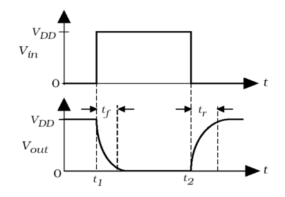
Figure 1. The input and output of CMOS inverter in practical (Photo/Picture credit: Original)
3.1. Transistor characteristics
To find out how the transistor characteristics affect the CMOS inverter switching delay, need to have a deep understanding to the CMOS inverter’s internal structure. The CMOS inverter’s internal structure is shown as follows in figure 2.
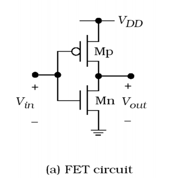
Figure 2. MOSFET circuit (Photo/Picture credit: Original)
Moreover, the equivalent circuit model using resistors, capacitors, and switches instead of CMOS tubes is shown as follows in figure 3.
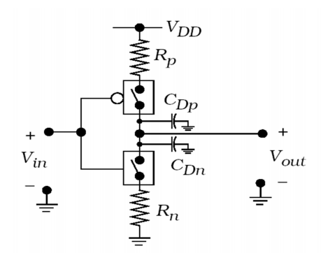
Figure 3. RC switch model equivalent (Photo/Picture credit: Original)
According to the equivalent internal structure in Figure 3, it is preliminarily inferred that the reason for the delay in the CMOS inverter is due to the presence of parasitic capacitance ( \( {C_{Dp}} \) , \( {C_{Dn}} \) ) and parasitic resistance ( \( {R_{p}} \) , \( {R_{n}} \) ) in the CMOS tube.
When the input \( {V_{in }} \) is high voltage ‘1’, the PMOSFET works in ‘off’ state but the NMOSFET works in ‘on’ state, and the parasitic capacitance begins to discharge. During the process of discharging the parasitic capacitor, the output voltage of the inverter gradually decreases, until all the electricity in the capacitor is discharged, then the inverter output becomes 0. Therefore, the output delay (falling-edge) of the inverter is the time required to discharge the parasitic capacitance. The falling time \( {t_{f}} \) is defined as the time for \( {V_{out}} \) to fall from 0.9 \( {V_{dd}} \) to 0.1 \( {V_{dd}} \) .
According to the capacitor charge and discharge formula [7].
\( f(t)=f(∞)+[f({0_{+}})-f(∞)]{e^{-\frac{t}{{τ_{n}}}}} (t \gt 0) \) (1)
Then get the discharge formula of parasitic capacitance:
\( {V_{out}}(t)=0+[{V_{dd}}-0]{e^{-\frac{t}{{τ_{n}}}}}={V_{dd}}{e^{-\frac{t}{{τ_{n}}}}} \) (2)
\( t=-{τ_{n}}ln{(\frac{{V_{out}}}{{V_{dd}}})} \) (3)
According to the definition of fall time, the fall time \( {t_{f}} \) is calculated:
\( {t_{f}}=t(0.1{V_{dd}})-t(0.9{V_{dd}})=-{τ_{n}}ln{(\frac{0.1{V_{dd}}}{{V_{dd}}})}+{τ_{n}}ln{(\frac{0.9{V_{dd}}}{{V_{dd}}})} \)
\( ={τ_{n}}ln{0.9}-{τ_{n}}ln{0.1}={τ_{n}}ln{9}≈2.2{τ_{n}} \) (4)
The steps to calculate the rise time are similar to the above. When \( {V_{in }} \) inputs low voltage 0, the PMOSFET works in ‘on’ state but the NMOSFET works in ‘off’ state, and the parasitic capacitance begins to charge. During the process of charging the parasitic capacitor, the voltage of the inverter output rises gradually, until the voltage across the capacitor equals \( {V_{dd}} \) , then the inverter output becomes 1. Therefore, the time of output delay (rising-edge) of inverter is the time required to charge the parasitic capacitance. The rising time \( {t_{r}} \) is defined as the time when \( {V_{out}} \) rises from 0.1 \( {V_{dd}} \) to 0.9 \( {V_{dd}} \) . Therefore, the charging formula for parasitic capacitance is obtained:
\( {V_{out}}(t)={V_{dd}}+[0-{V_{dd}}]{e^{-\frac{t}{{τ_{n}}}}}={V_{dd}}(1-{e^{-\frac{t}{{τ_{p}}}}}) \) (5)
\( t=-{τ_{p}}ln{(1-\frac{{V_{out}}}{{V_{dd}}})} \) (6)
According to the definition of rise time, the rise time \( {t_{r}} \) is calculated:
\( {t_{r}}=t(0.9{V_{dd}})-t(0.1{V_{dd}})=-{τ_{p}}ln{(1-\frac{0.9{V_{dd}}}{{V_{dd}}})}+{τ_{p}}ln{(1-\frac{0.1{V_{dd}}}{{V_{dd}}})} \)
\( ={τ_{p}}ln{0.9}-{τ_{p}}ln{0.1}={τ_{p}}ln{9}≈2.2{τ_{p}} \) (7)
According to the formula: \( τ=RC \) , it is not difficult for us to find the relationship between delay and resistance and capacitance [8]. Next, the influencing factors of parasitic capacitance and parasitic resistance will be analyzed separately.
3.1.1. Parasitic capacitance. When the input of the inverter changes, the parasitic capacitance needs to charge or discharge, causing a delay in signal propagation. The parasitic capacitance of a CMOS inverter primarily depends on the transistor size. Larger transistors typically have higher capacitance [9].
3.1.2. Parasitic resistance. To understand the impact of the size of the CMOS tube on delay, we need to further derive the relationship between the CMOS channel resistance and its size. Take the NMOSFET as an example:
The current flowing into the NMOS tube:
\( {I_{Dn}}≈{μ_{n}}{C_{ox}}\frac{W}{L}({V_{GSn}}-{V_{Tn}}){V_{DSn}} \) (8)
Define process conductance:
\( k_{n}^{ \prime }={μ_{n}}{C_{ox}} unit:A/{V^{2}} \) (9)
Define device mutual conductance:
\( {β_{n}}={μ_{n}}{C_{ox}}\frac{W}{L}=k_{n}^{ \prime }\frac{W}{L} unit:A/{V^{2}} \) (10)
Calculate its channel resistance according to Ohm’s law:
\( {R_{n}}=\frac{{V_{DSn}}}{{I_{Dn}}}=\frac{1}{{μ_{n}}{C_{ox}}\frac{W}{L}({V_{GSn}}-{V_{Tn}})}=\frac{1}{{β_{n}}({V_{GSn}}-{V_{Tn}})} \) (11)
\( {R_{n}}={R_{coefficient, n}}(\frac{L}{W}) \) \( {R_{coefficient,n}}=\frac{1}{{μ_{n}}{C_{ox}}({V_{GSn}}-{V_{Tn}})} \) (12)
The way to calculate the channel resistance in PMOSFET is the same:
\( {R_{p}}=\frac{{V_{SDp}}}{{I_{Dp}}}=\frac{1}{{μ_{p}}{C_{ox}}\frac{W}{L}({V_{SDp}}-|{V_{Tp}}|)}=\frac{1}{{β_{p}}({V_{SGp}}-|{V_{Tp}}|)} \) (13)
\( {R_{p}}={R_{coefficient, p}}(\frac{L}{W}) \) \( {R_{coefficient,p}}=\frac{1}{{μ_{p}}{C_{ox}}({V_{SDp}}-|{V_{Tp}}|)} \) (14)
According to the calculation formula of the channel resistance of the CMOS tube, the relationship between the channel resistance value and its size can be initially obtained. The channel resistance of a CMOS tube is proportional to its channel length but inversely proportional to its width[10]. Therefore, the resistance can be reduced by reducing the length of the channel or increasing the width of the channel during the design process to achieve the optimization effect.
3.1.3. Brief sum up. Thus, the relationship between the falling time, rising time and the size of CMOS can be found as follows:
\( {t_{r}}≈2.2{τ_{p}}={R_{p}}{C_{Dp}}=\frac{2.2}{{μ_{p}}{C_{ox}}({V_{SDp}}-|{V_{Tp}}|)}{(\frac{L}{W})_{p}}{C_{Dp}} \) (15)
\( {t_{f}}≈2.2{τ_{n}}={R_{n}}{C_{Dn}}=\frac{2.2}{{μ_{n}}{C_{ox}}({V_{GSn}}-{V_{Tn}})}{(\frac{L}{W})_{n}}{C_{Dn}} \) (16)
The calculation of this part of the delay will ignore the influence of the external load capacitance, that is, it is assumed that the load capacitance is 0. The effect of load capacitance on delay will be discussed in the next section.
According to the formula, it can be concluded that the CMOS rising and falling time is proportional to parasitic resistance and parasitic capacitance’s size. The size of the parasitic resistance is proportional to the size of the CMOS, that is, the aspect ratio. Therefore, the rise and fall time of CMOS is proportional to the aspect ratio of CMOS. At the same time, parasitic capacitance’s size also depends on the transistor’s size. Typically, the larger the transistor, the larger the parasitic capacitance.
3.2. Load capacitance
Load capacitance refers to the combined effect of the capacitance at the inverter output and the capacitance of the subsequent stages or connected elements in the circuit. When the inverter output switches, it needs to charge or discharge this load capacitance, influencing the overall delay [11].
The MOSFET circuit added with an external output capacitance is shown as follows in figure 4.
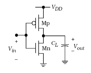
Figure 4. External load capacitance [11]
The RC switch model equivalent added with an external output capacitance is shown as follows in figure 5.
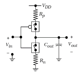
Figure 5. Complete switching model [11]
Total capacitance is the sum of all capacitances passing from input to output, which is the parasitic capacitance ( \( {C_{FET}} \) ) of the FET plus the load capacitance ( \( {C_{L}} \) ).
\( {C_{out}}={C_{FET}}+{C_{L}} \) (17)
\( τ=R{C_{out}} \) (18)
\( τ \) directly determines the rising and falling edge times.
In summary, a higher load capacitance results in a longer delay as more charge is required to change the output voltage. Properly reducing the capacitance connected to the output can reduce the switching delay to CMOS.
3.3. Propagation delay
The time difference between the moment when the input voltage becomes 50% \( {V_{dd}} \) and the moment when the output voltage becomes 50% \( {V_{dd}} \) is defined as the propagation delay of the inverter. The inverter’s propagation delay is shown as follows in figure 6.
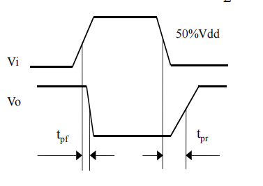
Figure 6. Propagation delay definition (Photo/Picture credit: Original)
However, such a delay is difficult to calculate. It is usually assumed \( {V_{in}} \) inputs an ideal step signal, and then calculate the average delay time of the inverter.
The CMOS inverter’s propagation delay is shown as follows when assuming \( {V_{in}} \) inputs an ideal step signal in figure 7.
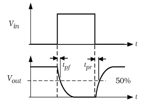
Figure 7. Propagation delay in CMOS inverter (Photo/Picture credit: Original)
The specific algorithm is as follows:
\( {t_{p}}=\frac{{t_{pf}}+{t_{pr}}}{2} \) (19)
From to the definition of propagation delay, the propagation fall time and propagation rise time can be calculated as follows:
When \( {V_{out}} \) changes from \( {V_{dd}} \) to \( 0.5{V_{dd}} \) , the \( {t_{pf}} \) is calculated as follows:
\( {t_{pf}}=t(0.5{V_{dd}})-t({V_{dd}})=-{τ_{n}}ln{(\frac{0.5{V_{dd}}}{{V_{dd}}})}+{τ_{n}}ln{(\frac{{V_{dd}}}{{V_{dd}}})} \)
\( ={τ_{n}}ln{1}-{τ_{n}}ln{0.5}={τ_{n}}ln{2}≈0.69{τ_{n}} \) (20)
When \( {V_{out}} \) changes from 0 to \( 0.5{V_{dd}} \) , the \( {t_{pr}} \) is calculated as follows:
\( {t_{pr}}=t(0.5{V_{dd}})-t(0{V_{dd}})=-{τ_{p}}ln{(1-\frac{0.5{V_{dd}}}{{V_{dd}}})}+{τ_{p}}ln{(1-\frac{0{V_{dd}}}{{V_{dd}}})} \)
\( ={τ_{p}}ln{1}-{τ_{p}}ln{0.5}={τ_{p}}ln{2}≈0.69{τ_{p}} \) (21)
Thus, the propagation delay can be calculated:
\( {t_{p}}=\frac{{t_{pf}}+{t_{pr}}}{2}=\frac{ln{2}}{2}({τ_{n}}+{τ_{p}})≈0.35({τ_{n}}+{τ_{p}}) \) (22)
According to previous calculations, the factors that affect \( τ \) are the aspect ratio of CMOS and the size of the transistor. Therefore, the transmission delay of CMOS is also affected by the aspect ratio and transistor size.
4. Conclusion
The present study provides a comprehensive analysis of the factors contributing to the switching delay in Complementary Metal-Oxide-Semiconductor (CMOS) inverters, which play a crucial role in contemporary digital circuits. The main objective of this research is to identify and examine both intrinsic and extrinsic factors that impact the switching delay of CMOS inverters, while proposing strategies for optimizing these delays to enhance the overall performance and energy efficiency of digital circuits.
The paper commences with an introduction that emphasizes the significance of CMOS technology in digital systems and the importance of comprehending and mitigating CMOS inverter switching delays to minimize energy consumption. The CMOS inverter plays a critical role in converting input signals into their complementary outputs, but this process is often impeded by switching delays. Thorough analysis is conducted on key factors contributing to these delays, including inherent factors such as transistor characteristics (threshold voltage, channel length and width, mobility), propagation delay, as well as external influences like load capacitance, supply voltage, temperature, process variations, and technology scaling. Section 3 presents meticulous analyses and calculations pertaining to the three primary influencing factors: transistor characteristics, additional capacitors connected to the output, and propagation delay. This study explores how these factors individually and collectively impact the switching delay of the CMOS inverter while providing optimization suggestions. The analysis encompasses discussions on parasitic capacitance and resistance along with their dependencies on transistor size and geometry. Furthermore, it delves into the effects of external load capacitance on delay while emphasizing the significance of reducing capacitance connected to the output for minimizing switching delays.
In summary, a comprehensive understanding of CMOS inverter delay and its influencing factors is crucial for the development of energy-efficient digital systems. Addressing these challenges necessitates a multidisciplinary approach encompassing advancements in semiconductor technology, circuit design strategies, and system-level optimization. As research and innovation continue to progress, there are promising prospects for enhancing the performance of digital circuits while significantly reducing energy consumption, thereby ushering in a new era of efficient and responsive electronic devices.
References
[1]. Nabavi-Lishi A, Rumin N C. Inverter models of CMOS gates for supply current and delay evaluation. IEEE Transactions on Computer-Aided Design of Integrated Circuits and Systems, 1994, 13(10): 1271-1279.
[2]. Ershov M, Liu H C, Li L, et al. Negative capacitance effect in semiconductor devices. IEEE Transactions on Electron devices, 1998, 45(10): 2196-2206.
[3]. Bisdounis L, Nikolaidis S, Koufopavlou O. Analytical transient response and propagation delay evaluation of the CMOS inverter for short-channel devices. IEEE Journal of Solid-State Circuits, 1998, 33(2): 302-306.
[4]. Adler V, Friedman E G. Delay and power expressions for a CMOS inverter driving a resistive-capacitive load. Analog Integrated Circuits and Signal Processing, 1997, 14: 29-39.
[5]. Daga J M, Ottaviano E, Auvergne D. Temperature effect on delay for low voltage applications [CMOS ICs]. Proceedings Design, Automation and Test in Europe. IEEE, 1998: 680-685.
[6]. Anis M, Allam M, Elmasry M. Impact of technology scaling on CMOS logic styles. IEEE Transactions on Circuits and Systems II: Analog and Digital Signal Processing, 2002, 49(8): 577-588.
[7]. Westerlund S, Ekstam L. Capacitor theory. IEEE Transactions on Dielectrics and Electrical Insulation, 1994, 1(5): 826-839.
[8]. Zafarkhah E, Maymandi-Nejad M, Zare M. Improved accuracy equation for propagation delay of a CMOS inverter in a single ended ring oscillator. AEU-International Journal of Electronics and Communications, 2017, 71: 110-117.
[9]. Lacord J, Ghibaudo G, Boeuf F. Comprehensive and accurate parasitic capacitance models for two-and three-dimensional CMOS device structures. IEEE Transactions on Electron Devices, 2012, 59(5): 1332-1344.
[10]. An T Y, Choe K K, Kwon K W, et al. Performance optimization study of FinFETs considering parasitic capacitance and resistance. Journal of semiconductor technology and science, 2014, 14(5): 525-536.
[11]. Jeppson K O. Modeling the influence of the transistor gain ratio and the input-to-output coupling capacitance on the CMOS inverter delay. IEEE Journal of Solid-State Circuits, 1994, 29(6): 646-654.Dorman L I 1975 Variations of Galactic Cosmic Rays (Moscow: Moscow State UniversityPress) p 103
Cite this article
Wu,C. (2024). Reduce energy consumption - causes of CMOS inverter switching delay and its influencing factors. Applied and Computational Engineering,78,67-75.
Data availability
The datasets used and/or analyzed during the current study will be available from the authors upon reasonable request.
Disclaimer/Publisher's Note
The statements, opinions and data contained in all publications are solely those of the individual author(s) and contributor(s) and not of EWA Publishing and/or the editor(s). EWA Publishing and/or the editor(s) disclaim responsibility for any injury to people or property resulting from any ideas, methods, instructions or products referred to in the content.
About volume
Volume title: Proceedings of the 2nd International Conference on Mechatronics and Smart Systems
© 2024 by the author(s). Licensee EWA Publishing, Oxford, UK. This article is an open access article distributed under the terms and
conditions of the Creative Commons Attribution (CC BY) license. Authors who
publish this series agree to the following terms:
1. Authors retain copyright and grant the series right of first publication with the work simultaneously licensed under a Creative Commons
Attribution License that allows others to share the work with an acknowledgment of the work's authorship and initial publication in this
series.
2. Authors are able to enter into separate, additional contractual arrangements for the non-exclusive distribution of the series's published
version of the work (e.g., post it to an institutional repository or publish it in a book), with an acknowledgment of its initial
publication in this series.
3. Authors are permitted and encouraged to post their work online (e.g., in institutional repositories or on their website) prior to and
during the submission process, as it can lead to productive exchanges, as well as earlier and greater citation of published work (See
Open access policy for details).
References
[1]. Nabavi-Lishi A, Rumin N C. Inverter models of CMOS gates for supply current and delay evaluation. IEEE Transactions on Computer-Aided Design of Integrated Circuits and Systems, 1994, 13(10): 1271-1279.
[2]. Ershov M, Liu H C, Li L, et al. Negative capacitance effect in semiconductor devices. IEEE Transactions on Electron devices, 1998, 45(10): 2196-2206.
[3]. Bisdounis L, Nikolaidis S, Koufopavlou O. Analytical transient response and propagation delay evaluation of the CMOS inverter for short-channel devices. IEEE Journal of Solid-State Circuits, 1998, 33(2): 302-306.
[4]. Adler V, Friedman E G. Delay and power expressions for a CMOS inverter driving a resistive-capacitive load. Analog Integrated Circuits and Signal Processing, 1997, 14: 29-39.
[5]. Daga J M, Ottaviano E, Auvergne D. Temperature effect on delay for low voltage applications [CMOS ICs]. Proceedings Design, Automation and Test in Europe. IEEE, 1998: 680-685.
[6]. Anis M, Allam M, Elmasry M. Impact of technology scaling on CMOS logic styles. IEEE Transactions on Circuits and Systems II: Analog and Digital Signal Processing, 2002, 49(8): 577-588.
[7]. Westerlund S, Ekstam L. Capacitor theory. IEEE Transactions on Dielectrics and Electrical Insulation, 1994, 1(5): 826-839.
[8]. Zafarkhah E, Maymandi-Nejad M, Zare M. Improved accuracy equation for propagation delay of a CMOS inverter in a single ended ring oscillator. AEU-International Journal of Electronics and Communications, 2017, 71: 110-117.
[9]. Lacord J, Ghibaudo G, Boeuf F. Comprehensive and accurate parasitic capacitance models for two-and three-dimensional CMOS device structures. IEEE Transactions on Electron Devices, 2012, 59(5): 1332-1344.
[10]. An T Y, Choe K K, Kwon K W, et al. Performance optimization study of FinFETs considering parasitic capacitance and resistance. Journal of semiconductor technology and science, 2014, 14(5): 525-536.
[11]. Jeppson K O. Modeling the influence of the transistor gain ratio and the input-to-output coupling capacitance on the CMOS inverter delay. IEEE Journal of Solid-State Circuits, 1994, 29(6): 646-654.Dorman L I 1975 Variations of Galactic Cosmic Rays (Moscow: Moscow State UniversityPress) p 103