


1. Introduction
The meaning of parasitic is that there is no capacitor designed in that place, but because there is always mutual capacitance between the wiring, mutual capacitance is like parasitic between the wiring, so it is called parasitic capacitance, also known as stray capacitance.
The parasitic capacitor itself is not a capacitor, according to the principle of capacitance we can know that the capacitor is composed of two plates and insulating media, so the parasitic capacitor is unavoidable. For example, a circuit has many wires, and the capacitance formed between the wires and wires is called parasitic capacitance. Parasitic capacitors generally have a great impact on the circuit in high-frequency circuits, so special consideration should be given to the circuit when wiring.
Parasitic capacitance generally refers to the capacitance characteristics of inductors, resistors, chip pins, etc. displayed at high frequencies. In fact, a resistor is equivalent to a capacitor, an inductor, and a series of resistors, which is not very obvious at low frequencies, and at high frequencies, the equivalent value will increase and cannot be ignored. We have to take that into account in the calculation. ESL is equivalent inductance, ESR is equivalent resistance. Whether it is resistance, capacitor, inductor, or diode, transistor, MOS tube, and IC, in the case of high frequency we have to take into account their equivalent capacitance value, inductance value [1].
Pay attention to the stray capacitor, parasitic capacitor, distributed capacitor these three statements, some people think that the three statements are not very different, but the application scenario is different, for the device when the use of "parasitic capacitor", for the system when the use of "distributed capacitor". In my understanding, there are some subtle differences between the three.
Parasitic capacitance: At the level of modern technology, another phenomenon that is inevitably produced when producing a certain function of the device, such as the modern production of diodes, due to process limitations, there is no way to make an ideal diode, and capacitance is inevitably generated during production.
It is certain that parasitic capacitors are harmful in many aspects of production forging. For example, for an initial capacitor, the capacitance is not zero or even quite large when the variable capacitor's rotor is fully rotated out. This is because the moving disc, the shaft and the bottom shell of the general variable capacitor are connected. Although the moving disc is completely rotated out, there is a gap between the shaft and the fixing plate, there is still a considerable amount of parasitic capacitance between the stator and the bottom shell through the insulator. The capacitance of the stator pair and the stator pair in parallel are called the "Starting capacitance" of the variable capacitor, typically 10 to 50 micrometers. The initial capacitance narrows the tuning range of the oscillating circuit, especially so that it cannot be used at higher frequencies. The variation of initial capacitance with temperature is also the main reason for the instability of oscillation frequency.
Parasitic capacitors also produce a phenomenon called parasitic oscillations: sometimes the radio makes a harsh sound, this is often due to parasitic oscillations caused by positive feedback from parasitic capacitors or inductors in the low-frequency part. For example, when the lead of the output transformer is close to the lead of the first low amplifier stage, it becomes positive feedback through parasitic capacitance and double amplification inversion. If we pull the two most critical wires apart to remove the parasitic capacitance, the positive feedback path is cut and the howling stops.
Similarly, parasitic capacitors can cause high-frequency gain drops: in general, the gain of a low-frequency amplifier decreases as the frequency increases, this is because the amplifier load in parallel with the parasitic capacitance (including the lower electron tube of the inter-electrode capacitance, installation capacitance, lead capacitance, etc.). The higher the frequency, the lower the capacitance impedance, and the more high-frequency current flows directly from the parasitic capacitor to the ground, so that the high-frequency gain (magnification) falls down. It has been pointed out previously that the parasitic capacitance between conductors inside and outside the shield line is large, and if the shield line is connected to the gate of a high frequency amplifier, it is equivalent to increasing its input capacitance, and the magnification is expected to be greatly reduced, as a result, the sensitivity of the amplifier decreases.
The dangers of parasitic capacitors and the ways to combat them in radio equipment are innumerable. In short, in the use of high-frequency signals, the use of new structures, trial-manufacture of new equipment, the components, devices, mechanical installation of the various parts of the parasitic capacitance must be taken into account. Additional facilities such as shielding and compensation can be used when necessary [2].
2. Some theoretical methods of reducing parasitic capacitance
In theory, there are several ways to reduce parasitic capacitance:
2.1. Increasing the initial capacitance value
By increasing the initial capacitance, the capacitance of the parasitic capacitance can be reduced relative to that of the capacitance sensor. From the formula
\( C0=\frac{ε0\cdot εr \cdot A}{d0}\ \ \ (1) \)
It can be concluded that the distance between the two electrodes can be reduced by d0, for example, the distance between the plate electrodes can be reduced to 0.2 mm, the distance between the cylinder electrodes can be reduced to 0.15 mm, or a layer of glass medium can be covered between the two electrodes, in order to improve the relative permittivity, it is found that the initial capacitance C0 of the sensor is not only significantly increased, but also to prevent the short circuit between the two electrodes in case of overload, increasing working area A or working length also increases the initial capacitance value C0. However, this method is limited by the machining process and assembly process, precision, indication range, breakdown voltage, etc.
2.2. Adopt “Drive cable” technology to reduce parasitic capacitance
As shown in Figure 1: Between the piezoelectric sensor and amplifier A, a double-shielded cable is connected to the driver amplifier with a gain of 1, furthermore, the capacitive leakage of the core wire to the inner shield is eliminated, and the influence of the parasitic capacitance is overcome, and the capacitance CX between the inner and outer layers becomes the load of the driving amplifier, its capacity is very small, generally only a few pF to dozens of pF. Because C is too small, the capacitive resistance
\( Xc=\frac{1}{2π\cdot f\cdot C}\ \ \ (2) \)
is very large and is a high impedance element. Therefore, the drive amplifier can be seen as a high input impedance, and a capacitive load, the amplifier magnification of 1 in-phase amplifier.[3]
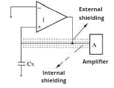
Figure 1. Driving amplifier schematic diagram
And for reducing the parasitic capacitance on the capacitance sensor, there are two other practical methods.
3. The operational amplifier method
Using "Drive cable" method to eliminate parasitic capacitance is to realize the amplifier magnification equal to 1 in a wide frequency band, and the phase shift of input and output is zero. The operational amplifier method can effectively solve this problem. As shown in Figure 2: (- Aa) for the drive cable amplifier, its input is the output of (- A) amplifier, (- Aa) amplifier's input capacitance is (- A) amplifier load, so no additional capacitance and CX parallel, the sensor capacitor CX has two terminal voltages of
\( Ucx=U01-U02=U01-(-A\cdot U01)=(1+A)\cdot U01\ \ \ (3) \)
The output voltage of the amplifier (- Aa) is
\( U03=-Aa\cdot U02=A\cdot Aa\cdot U01\ \ \ (4) \)
To achieve the equality of the cable core and the inner shield potential, Ucx = Uo3 should be made so that:
\( (1+A)\cdot U01=A\cdot Aa\cdot U01\ \ \ (5) \)
So
\( Aa=1+\frac{1}{A}\ \ \ (6) \)
The method does not have any additional capacitance, and is especially suitable for the detection circuit when the capacitance of the sensor is very small.
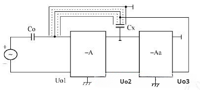
Figure 2. Schematic diagram of sensor circuit
4. Integral shielding method
Shielding technology is the use of metal materials for electromagnetic wave has good absorption and reflection ability to carry out anti-interference. According to the characteristics of electromagnetic interference, choose a good low resistance conductive material or magnetic conductive material to form a suitable shield. The shield acts as a parallel short circuit between two ends of an equivalent resistance, passing directly through the short circuit when unwanted signals enter in series, without affecting the equivalent resistance. This paper takes the differential capacitance sensor as an example to illustrate the application of the whole shielding method. In Figure 3, CX1 and CX2 act as differential capacitors, U as power supply, and a as amplifier. The whole shielding method is to shield the whole bridge (including power cable, etc.) in the drawing. The key point of this method is the reasonable setting of grounding point. The grounding point is placed between the two balance resistors, R1 and R2, and is cogrounded with the overall shield. Thus, the parasitic capacitance C1 between the common plate and the shield of the sensor is connected in parallel with the input impedance of the measuring amplifier, so that C1 can be regarded as the input capacitance of the amplifier. Since the input impedance of the amplifier should have a great value, the parallel connection of C1 is not desirable, but it only affects the sensitivity of the sensor, and has no effect on other performance. The other two parasitic capacitors, C3 and C4, are connected in parallel to the two arms, R1 and R2, respectively. This will affect the initial balance and overall sensitivity of the bridge, but will not affect the normal operation of the Wheatstone bridge bridge. Therefore, the effect of parasitic parameters on the capacitance of the sensor can be basically eliminated. The whole shield method is a good method to solve the parasitic capacitance problem of capacitance sensor.
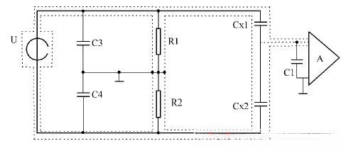
Figure 3. Schematic diagram of shield circuit
In addition, integration method is also an effective method to eliminate parasitic capacitance interference of capacitance sensor. In this method, the sensor and the front stage of the electronic circuit are packaged together in a shell, and the cable from the sensor to the front amplifier is omitted. In this way, the parasitic capacitance can be greatly reduced and kept fixed, keep the instrument in a stable working state. However, this practice because of the existence of electronic components cannot be in a relatively high temperature or harsh environment where normal use. The integrated capacitance sensor can also be formed by integrating the sensor and the conditioning circuit on the same chip.
In a word, the capacitance of capacitive sensors is very small, usually at the pF level, and the distributed capacitance produced by the connecting line is also at the pF level, which will affect the measurement accuracy, therefore, it is required that the connection between the sensor and the conversion circuit should choose their own high-frequency cable with very small distributed capacitance, and also try to shorten the distance between the sensor and the conversion circuit, when conditions are available, the sensor, the connecting wire and the conversion circuit can be shielded as a whole [4].
In particular, with the increasing use of PCB, it is necessary to emphasize on how to reduce the parasitic capacitance on PCB.
Due to recent trends, improving efficiency has become a key goal and the tradeoff between using slow switching devices and better EMI is not worth it. Superjunctions can enhance efficiency in applications where planar MOSFETs would not be suitable. Compared to traditional planar MOSFET technology, superjunction MOSFETs offer substantial advantages, notably reducing on-resistance and parasitic capacitance. While this reduction enhances efficiency, it also introduces challenges related to rapid voltage (dv/dt) and current (di/dt) switching transitions, leading to elevated high-frequency noise and electromagnetic radiation emissions.
To effectively drive fast-switching superjunction MOSFETs, it's crucial to comprehend the impact of PCB packaging and parasitic layouts on switching performance and the necessary PCB layout adjustments for optimal superjunction utilization. Superjunction MOSFETs, typically with breakdown voltages ranging from 500 to 600 V, are the predominant choice. Within this voltage range, industry-standard packages like TO-220, TO-247, TO-3P, and TO-263 are commonly employed.
Packaging has limited impact on performance because the lengths of the internal gate and source bonding wires are fixed. Only the wire size can be changed to reduce the inductance of the package source. As shown in Figure 1(a), a typical 10 nH lead inductor may not seem like much, but the di/dt of these MOSFETs can easily reach 500 A/μs! Assuming that di/dt is 500A/μs, the voltage across the 10nH line inductor is VIND=5V and the turn-off di/dt of the 10nH line inductor is 1000A/μs, which is a voltage of VIND can produce =10V. In most applications and designs, this additional inductance is not considered a voltage but cannot be ignored. The above simple calculation shows that the total inductance of the package source, i.e. H. the inductance of the jumper cable and pins should be reduced to an acceptable value. Another source of noise is layout noise. There are two visible parasitic configurations: parasitic inductance and parasitic capacitance. The inductance of a 1 cm trace is 6 to 10 nH; This inductance value can be reduced by adding a layer above the PCB and a GND layer at the bottom of the PCB. Another type is parasitic capacitance. Figure 1 (b) shows the principle of capacitive interference in the network. A stray capacitance occurs between two adjacent conductor tracks or a conductor track and the ground plane on the other side. Another type of capacitance is between the device and the ground plane. Two parallel traces on both sides of the circuit board can increase capacitance and reduce loop inductance, thereby reducing electromagnetic radiation. Next time your design requires superjunction MOSFETs, consider these layout tips.
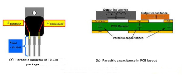
Figure 4. Parasitic components in packaging and layout
Superjunction MOSFETs, due to their unipolar nature, grapple primarily with limitations in switching transients driven by parasitic capacitance. Employing the charge balancing principle allows for a reduction in area-specific on-resistance, resulting in smaller chip sizes for equivalent RDS(ON) compared to standard MOSFET technology. Notably, Figure 1 illustrates the capacitance characteristics of superjunction MOSFETs and standard planar MOSFETs, with the former exhibiting a highly nonlinear Coss curve that initially starts with a high value but rapidly drops at a drain-source voltage of around 50V. When applied in PFC or DC/DC converter applications, these nonlinear effects can instigate voltage and current oscillations, as demonstrated in Figure 3, which presents a simplified PFC circuit schematic incorporating both internal parasitic components of the power MOSFET and external oscillation circuit, including the impact of external coupling capacitance (Cgd_ext) introduced by layout considerations.

Figure 5. Comparison of output capacitance of planar MOSFET and super junction MOSFET
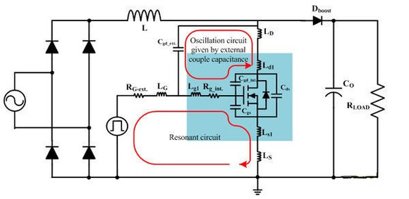
Figure 6. Simplified PFC circuit including internal and external parasitic components of the power MOSFET
Multiple oscillation circuits, both internal and external, impact MOSFET switching characteristics. Figure 3's PFC circuit (comprising L, Co, and Dboost) features the inductor, output capacitor, and boost diode. Additionally, parasitic capacitances are associated with the power MOSFET, including Cgs, Cgd_int, and Cds. The power MOSFET's drain, source, and gate bonding wires and pin inductance are represented by Ld1, Ls1, and Lg1. Internal gate resistance (Rg_int) and external gate drive resistance (Rg_ext) also play a role. Cgd_ext denotes the parasitic gate-drain capacitance in the circuit.
Furthermore, during MOSFET switching, gate parasitic oscillations arise within the resonant circuit through the interaction of gate-drain capacitance (Cgd) and gate lead inductance (Lg1). Additionally, printed circuit board (PCB) trace stray inductances, denoted as LD, LS, and LG, contribute to these dynamics.
Under resonant conditions
\( ωL=\frac{1}{ωC}\ \ \ (7) \)
The oscillating voltage generated in the gate and source voltages is much larger than the driving voltage. The voltage oscillation caused by the resonance change is proportional to the quality factor
\( Q=\frac{ωL}{R}=\frac{1}{ωC\cdot R}\ \ \ (8) \)
When the MOSFET is turned off, the drain parasitic inductance (LD + Ld1), gate-drain capacitance Cgd, and gate lead inductance Lg1 network cause the gate oscillation voltage. Q becomes large if the gate resistance (RG-ext.+Rg_int.) is minimal. In addition, the voltage drop across LS and the stray inductance of the source of Ls1 produce oscillation in the gate-source voltage, which can be expressed by expression (1). Parasitic oscillation may cause gate-source breakdown, harmful EMI, significant switching losses, gate control failure, and even MOSFET failure.
\( ΔVgs=(Ls+Ls1)\cdot \frac{did(t)}{dt}\ \ \ (9) \)
It is essential to optimize circuit design to maximize the performance of superjunction MOSFETs without negative impacts [5].
5. Conclusion
Parasitic meaning is not designed in that place, but because there is always mutual tolerance between the wiring, mutual tolerance is like parasitic in the wiring between the same, so-called parasitic capacitance. All practical circuit elements such as inductors, diodes, and transistors have internal capacitors that cause them to behave in ways that deviate from the behavior of ideal circuit elements. In addition, there is always a non-zero capacitance between any two conductors; this may be important for conductors that are closely spaced, such as wires or printed circuit board wiring. However, complete elimination of parasitic capacitors is not possible, so we can only minimize their impact.
References
[1]. 360 encyclopedias (2022). Parasitic capacitance. https://baike.so.com/ doc/8489616-8809829.html
[2]. h1654155282 (2020). What is a parasitic capacitor_ The perils of parasitic capacitors. https://m.elecfans.com/article/1300141.html
[3]. zxx7366812 (2017). How to eliminate the effect of parasitic capacitance. https://wenda.so.com/q/1515027866215009
[4]. Network collation (20). Operational amplifier method-causes and elimination of parasitic capacitance interference https://www.elecfans.com/yuanqijian/dianrongqi/20180131 6269242.html
[5]. Namowentilaila (2015). How to optimize the PCB design to maximize the performance of super junction MOSFET https://tieba.baidu.com/p/3916933910?pid=72134774156&cid=0#72134 774156
Cite this article
Bao,C.;Zhu,H.;Liu,J. (2024). Introduction of parasitic capacitance and methods of reducing its capacitance. Applied and Computational Engineering,85,141-147.
Data availability
The datasets used and/or analyzed during the current study will be available from the authors upon reasonable request.
Disclaimer/Publisher's Note
The statements, opinions and data contained in all publications are solely those of the individual author(s) and contributor(s) and not of EWA Publishing and/or the editor(s). EWA Publishing and/or the editor(s) disclaim responsibility for any injury to people or property resulting from any ideas, methods, instructions or products referred to in the content.
About volume
Volume title: Proceedings of the 4th International Conference on Materials Chemistry and Environmental Engineering
© 2024 by the author(s). Licensee EWA Publishing, Oxford, UK. This article is an open access article distributed under the terms and
conditions of the Creative Commons Attribution (CC BY) license. Authors who
publish this series agree to the following terms:
1. Authors retain copyright and grant the series right of first publication with the work simultaneously licensed under a Creative Commons
Attribution License that allows others to share the work with an acknowledgment of the work's authorship and initial publication in this
series.
2. Authors are able to enter into separate, additional contractual arrangements for the non-exclusive distribution of the series's published
version of the work (e.g., post it to an institutional repository or publish it in a book), with an acknowledgment of its initial
publication in this series.
3. Authors are permitted and encouraged to post their work online (e.g., in institutional repositories or on their website) prior to and
during the submission process, as it can lead to productive exchanges, as well as earlier and greater citation of published work (See
Open access policy for details).
References
[1]. 360 encyclopedias (2022). Parasitic capacitance. https://baike.so.com/ doc/8489616-8809829.html
[2]. h1654155282 (2020). What is a parasitic capacitor_ The perils of parasitic capacitors. https://m.elecfans.com/article/1300141.html
[3]. zxx7366812 (2017). How to eliminate the effect of parasitic capacitance. https://wenda.so.com/q/1515027866215009
[4]. Network collation (20). Operational amplifier method-causes and elimination of parasitic capacitance interference https://www.elecfans.com/yuanqijian/dianrongqi/20180131 6269242.html
[5]. Namowentilaila (2015). How to optimize the PCB design to maximize the performance of super junction MOSFET https://tieba.baidu.com/p/3916933910?pid=72134774156&cid=0#72134 774156