


1. Introduction
In modern integrated circuit design, there are often multiple clocks in the chip to control data transfer. The transfer of data under the control of different clocks requires the modules to be interconnected and requires a high degree of precision as well as transfer efficiency. For this reason, it is important to design a means of storing and transmitting data between different clocks. Under the multi-clock domain, asynchronous FIFO can realize the control of the asynchronous interface between two clocks for data transmission between different clocks. Tan in order to design a fiber grating sensor with a data acquisition function [1], the use of asynchronous FIFO system as the grassroots means of transmission, and successfully achieved low-power high-speed acquisition at the same time to achieve the function of high sampling rate. Asynchronous FIFO not only effectively alleviates the timing requirements, but also solves the problems of clock difference between reference clocks, between local and remote, as well as the problem of metastable state [2].
Designing an efficient asynchronous FIFO program is the key to achieving data transfer across different clocks. To address the phenomenon of data transfer generating sub-stability across different clock regions and the way to address the read-empty and write-full representations, the program optimization process is written, and relevant experimental data is obtained.
Comparing the counter method and the expand-high-pointer method in synchronous FIFO design, since it is more difficult to distinguish the counting increment and decrement between different clocks in asynchronous FIFO, choosing the counter method is a difficult and low-value choice. For this reason, the expansion of the high-bit pointer method is used for the design, the address pointer is expanded by one bit as an indication bit, while comparing the value of the read and write pointers to determine the read empty and write full. In this paper, the expanded high-bit pointer method is used as the basis to write in Verilog language on a notepad, and the result of the writing is run on models for simulation to get the data.
This research is based on the writing of an asynchronous FIFO program to achieve low BER, optimizing the program and reducing the delay in data transmission if the program is implemented and the simulation results are error-free, obtaining the improved program and further checking the BER.
2. Theoretical foundations
2.1. FIFO module
FIFO is a first-in-first-out dual-port data buffer that enables sequential writing of data and sequential reading of data with reduced input signal control lines. The framework of this asynchronous FIFO program is shown in Fig 1.
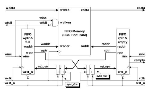
Figure 1. Basic framework diagram of asynchronous FIFO [3].
The above is the basic FIFO program implementation diagram. The depth of this FIFO is 4 and the bit width is 2^4.In order to implement the FIFO, a total of five aspects of the module need to be designed, which are Dual Port Storage RAM, Read Controller, Write Controller, R2W Synchronizer, and W2R Synchronizer [4].
The read/write controller determines and generates read/write pointer signals when read/write signals and enable signals to occur, and inputs them into the memory RAM.
The storage RAM consists of groups of registers. Input data is written to the storage unit when the write signal is valid and read from the storage signal when the read clock signal is valid. When data is written or read, the read and write addresses are automatically totalized [4]. R2W and W2R synchronizer roles are similar, R2W is the read counter synchronized to the write clock domain, after the synchronization of the signal and write binary counter comparison, to determine whether it has been in the write state, synchronized to the write state flag bit and data output. Similarly, W2R synchronizes the write counter to the read clock domain and then compares it with the read binary counter to determine whether it is in the read empty state, synchronizes it to the read state flag bit, and performs data output.The read and write flag bits are used to generate read-empty and write-full signals and transfer data to the module.
The pinout of this program is shown in Table 1.
Table 1. Asynchronous FIFO pins.
pinout |
I/O |
functionality |
wr_full |
O |
Full flag bit, active high |
rd_empty |
O |
Empty flag bit, active high |
wr_en |
I |
Write enable signal, active high |
rd_en |
I |
Read enable signal, active high |
wrclk |
I |
Write Clock Signal |
rdclk |
I |
Read Clock Signal |
wr_rst_n |
I |
Write Reset Signal |
rd_rst_n |
I |
Read reset signal |
wr_data |
I |
Write Input Data |
rd_data |
O |
Read Output Data |
2.2. Procedural difficulties
As for the key part, it is to design the R2W module and W2R module, so that the read and write clock domains are synchronized [5]. In this, it is inevitable to encounter data transmission, “the report of the empty full but not reported”, this is the impact of the data transmission caused by the substable state. If a data signal before the change does not meet the requirements of the flip-flop establishment and hold time, the output of the flip-flop may enter the substable state [6]. The details are shown in Fig 2.
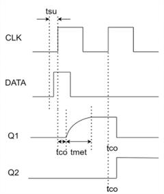
Figure 2. Generation of sub-stable states.
It can be seen that in order to achieve the read and write pointer values synchronized to the same clock domain, the use of binary pointer conversion to Gray code this way, can effectively reduce the generation of substability. Gray code is a non-weighted code, each time the value changes only one digital change, compared to the binary code each time the change of 1 to 4 bits, Gray code in this way to determine the read empty and write full of this way the error tolerance will become very high, there will not be a “report empty and full and did not report” this situation. In this writing, Gray code operation is shown in Fig 3.
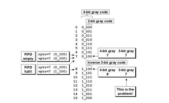
Figure 3. Example of empty-full judgment diagram using Gray code [7].
After the selection of the Gray code conversion method, data transmission when the generation of substability problem can be initially solved, can be seen in order to further reduce the impact of substability, the use of two-level registers to store data, can reduce the probability of substability. The two-level register is in the case of different clock domains input data, the data of each clock domain latches two beats, when the first clk is the rising edge of the data collection, at this time if the second clk is also in the rising edge, will be collected a change of data1, trigger 1 is in the suitable state. But with the use of a secondary latch, the clock will be delayed by one beat, this time data1 will tend to stabilize, and trigger 2 at this time on the stabilization of data1 collection, the output data2 will become a certain value. This way can effectively reduce the impact of the substable state.
Next is the relationship between the read-empty and write-full states. Here is used to increase the flag bit, when read empty and write full, read empty flag bit and write full flag bit will become high. At this time, if the read and write the highest bit is the same and the rest of the bit is also the same, the judgment is read empty. If the highest and second highest bits are different and the rest of the bits are the same, it will be judged as written fully.
3. Program implementation
3.1. FIFO variable definition
Parameter WIDTH = 16, parameter PTR = 4 parameter PTR = 4 Defines a FIFO depth of 4, a bit width of 2^4, and the amount of inputs and outputs required by each read and write controller.
3.2. Read empty judgment module
The inputs are synchronized write pointer, read enable signal, read clock, read reset signal, and the outputs are read address and read null signal.
When the stored data rd_empty == 1’b0 is not empty and there is a read enable signal rd_en == 1’b1 input, the read pointer is added 1.
The read pointer signal is later converted to Gray code. The Gray code essence rd_gray <= { rd_bin[PTR], rd_bin[PTR:1] ^ rd_bin[PTR-1:0] } is a bitwise dissimilarity between the binary code and the binary code of the right one bit, and the data obtained is the Gray code converted to. [7]
The resulting Gray code is placed in a secondary register to minimize the probability of metastable state.
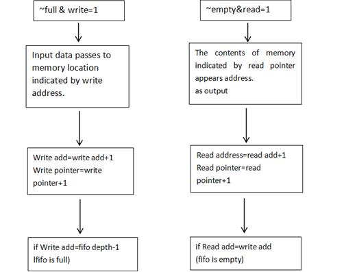
Figure 4. The nature of Gray’s code applied to the conversion in FIFO [7].
After getting the Gray code, judge whether wr_bin_rd == rd_bin, the read pointer signal is the same as the synchronized write pointer signal, and if it is the same, the read empty signal rd_empty is set to 1.
3.3. Write full judgment module
It is basically the same as the Read Empty Judgment Module, which compares the write signal converted to Gray code with the synchronized read pointer.
The point of difference is that the judgment condition is different, it is compare (wr_bin[PTR] ! = rd_bin_wr[PTR]) && (wr_bin[PTR-1:0] == rd_bin_wr[PTR-1:0]), read and write pointers are the same in the highest bit and the second highest bit and the rest of the bits are different, the write pointer overruns the read pointer by one turn, and the write signal wr_full = 1’b1 is output.
3.4. R2W read pointer synchronized write clock domain module
Rd_bin_wr[PTR] = rd_gray_ff2[PTR], Synchronize the read pointer to the write clock domain, output the write pointer signal, and the inputs are read clock, read pointer, and read reset signals.
The obtained Gray code rd_gray_ff1 <= rd_gray;rd_gray_ff2 <= rd_gray_ff1 is put into the second level register to synchronize the read pointer with the write clock domain in a second level register. The secondary register latches the input data for two beats, effectively reducing the probability of substability.
3.5. W2R write pointer synchronized read clock domain module
Consistent with the R2W Read Pointer Synchronization to Write Clock Domain module type, here the write pointer is synchronized to the read clock domain through a secondary register for conversion, after which the signal is fed into a RAM register.
4. Simulation test
After organizing the above code, make a simulation in the form of a tb file and test the results on the ModelSim software. Initialize the signals and set all signals except the reset signal to 0. Define wr_data <= $random, the input signal is a random variable. After that, write the program to save the 100 input signals and compare them with the output signals. If there is no difference between the 100 input signals and the output signals, the asynchronous FIFO program is considered to be running correctly and the output is “simulation is ok”, otherwise, the output is “simulation is wrong, error point is”, pointing out the place of error. If there is no difference between the 100 signal inputs and outputs, the asynchronous FIFO program is considered to be running correctly, and “simulation is ok” is the output.
The data waveform for a run of 1000us is as follows.
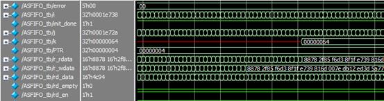
Figure 5. The first half of the simulation results.
At the beginning of the write data and read data in the middle of the delay, because at this time just write data running FIFO memory for the 2-level register beat and Gray code conversion and other operations, because of the situation. With the back of the read and write pointer synchronization data gradually flat.
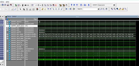
Figure 6. The second half of the simulation results.
The clock change and reset signals have waveform outputs, and the inputs of the write-full and read-null signals also have normal waveforms.
The data written and read are identical, and according to the results of running the code, it can be seen that the data input and output do meet the requirements of asynchronous FIFO, and the synchronization of data is achieved.
Looking at the read and write data inputs and outputs from Memory List, the 100 data for comparison are as follows.
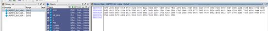

Figure 7. Comparison chart between input data and output data.
The results are consistent and it can be seen that with 100 data transfers in the test, there are almost no BERs.
5. Results and discussion
This asynchronous FIFO is written to solve the read-empty and write-full problems, utilizing binary to Gray code to binary to reduce the occurrence of suitable conditions, and also utilizing second-level registers to implement beat caching, which improves the stability of the code operation and increases the fault tolerance rate. The simulation results use the method of giving input data random variables and comparing them with output data to see if the asynchronous FIFO program successfully realizes the input and output of data across the clock domain. The asynchronous FIFO program accurately implements the data transfer function as viewed from the simulation graph results as well as the data memory area.
However, it is not difficult to see that the program has too long a lead time in transmitting the data because using a second-level register decreases the rate of transmitting the data while decreasing the incidence of substability. This is the classic sacrifice of validity for reliability within communication engineering.
Further, in order to make the function more comprehensive, there are also many ways to improve the program design, for example, the delay control module can be added to control the data transmission [8], and the anti-seu module to achieve resistance to single-particle inversion [9], can optimize the program design. For the results of this study, the design of the asynchronous FIFO program for the overall development of the chip to improve the data transmission module, such as literature [10], asynchronous FIFO used in the field of communication can be realized between the mailboxes to transfer information, for the use of electronic science in the transmission of data to lay a good foundation.
6. Conclusion
This research has refined the solution to the problem of transmitting data across clock domains with an asynchronous FIFO program. Starting from the study of the basic structure of asynchronous FIFO, we gradually analyze the knowledge and understanding required to design an asynchronous FIFO program and the difficulties that need to be overcome. After mastering the basic principles of Gray code and secondary latch to solve the substable problem, we began to write the program several times and modify the error reporting problem, and finally obtained the simulated experimental data and successfully measured the error code of data transmission in the case of the program running, so as to verify the solution of the substable problem.
This study provides a more accurate data transmission method in terms of communication software as well as data transmission code for chip fabrication, which can provide a certain basis and concept for complex circuit design. However, in terms of depth, the program obtained in this study still has a lot of room for improvement in terms of data transmission rate, which increases the transmission time to a certain extent while ensuring accuracy. In the future research direction, more modules can be added to reduce the lack of transmission rate, and other modules can also be added to realize the possibility of data transmission in different aspects.
References
[1]. Tan Ch 2023 Design of ping-pong mode high-speed data acquisition system based on STM32 with asynchronous FIFO. Electrotechnical Materials vol 01 p 55-59+63
[2]. Zhan Y Z 2022 A high-speed asynchronous FIFO for 100Gbit/s Ethernet PCS Microelectronics vol 52 no 5 p 886-892
[3]. Clifford E 2022 Simulation and synthesis techniques for asynchronous FIFO design SNUG 2002 Synopsys Users Group Conference vol 281
[4]. Ying X 2023 Asynchronous FIFO Design Based on Verilog Highlights in Science, Engineering and Technology vol 38 p 965-970
[5]. Zhang Z 2023 Optimization of Asynchronous FIFO Design Difficulties Using Verilog HDL Highlights in Science, Engineering and Technology vol 38 p 956-964
[6]. Li H Wang Q 2021 Asynchronous FIFO design based on Verilog HDL Electronic Design Engineering vol 29 no 19 p 107-111+116
[7]. Kumari P 2016 Implementation of asynchronous FIFO and interface it with UART Int J VLSI Syst Des Commun Syst vol 4 no 5 p 0390-0394
[8]. Chen T 2022 A delay-controlled asynchronous FIFO circuit design Microelectronics vol 52 no 01 p 42-46
[9]. Sun Y Ren Y Fan Y 2023 Asynchronous FIFO anti-SEU design Modern Electronic Technology vol 46 no 11 p 160-164
[10]. Hu D 2024 Review on the Usage of Synchronous and Asynchronous FIFOs in Digital Systems Design Engineering vol 16 no 3 p 61-82
Cite this article
Wu,H. (2024). Asynchronous FIFO module design and implementation. Applied and Computational Engineering,72,164-171.
Data availability
The datasets used and/or analyzed during the current study will be available from the authors upon reasonable request.
Disclaimer/Publisher's Note
The statements, opinions and data contained in all publications are solely those of the individual author(s) and contributor(s) and not of EWA Publishing and/or the editor(s). EWA Publishing and/or the editor(s) disclaim responsibility for any injury to people or property resulting from any ideas, methods, instructions or products referred to in the content.
About volume
Volume title: Proceedings of the 2nd International Conference on Functional Materials and Civil Engineering
© 2024 by the author(s). Licensee EWA Publishing, Oxford, UK. This article is an open access article distributed under the terms and
conditions of the Creative Commons Attribution (CC BY) license. Authors who
publish this series agree to the following terms:
1. Authors retain copyright and grant the series right of first publication with the work simultaneously licensed under a Creative Commons
Attribution License that allows others to share the work with an acknowledgment of the work's authorship and initial publication in this
series.
2. Authors are able to enter into separate, additional contractual arrangements for the non-exclusive distribution of the series's published
version of the work (e.g., post it to an institutional repository or publish it in a book), with an acknowledgment of its initial
publication in this series.
3. Authors are permitted and encouraged to post their work online (e.g., in institutional repositories or on their website) prior to and
during the submission process, as it can lead to productive exchanges, as well as earlier and greater citation of published work (See
Open access policy for details).
References
[1]. Tan Ch 2023 Design of ping-pong mode high-speed data acquisition system based on STM32 with asynchronous FIFO. Electrotechnical Materials vol 01 p 55-59+63
[2]. Zhan Y Z 2022 A high-speed asynchronous FIFO for 100Gbit/s Ethernet PCS Microelectronics vol 52 no 5 p 886-892
[3]. Clifford E 2022 Simulation and synthesis techniques for asynchronous FIFO design SNUG 2002 Synopsys Users Group Conference vol 281
[4]. Ying X 2023 Asynchronous FIFO Design Based on Verilog Highlights in Science, Engineering and Technology vol 38 p 965-970
[5]. Zhang Z 2023 Optimization of Asynchronous FIFO Design Difficulties Using Verilog HDL Highlights in Science, Engineering and Technology vol 38 p 956-964
[6]. Li H Wang Q 2021 Asynchronous FIFO design based on Verilog HDL Electronic Design Engineering vol 29 no 19 p 107-111+116
[7]. Kumari P 2016 Implementation of asynchronous FIFO and interface it with UART Int J VLSI Syst Des Commun Syst vol 4 no 5 p 0390-0394
[8]. Chen T 2022 A delay-controlled asynchronous FIFO circuit design Microelectronics vol 52 no 01 p 42-46
[9]. Sun Y Ren Y Fan Y 2023 Asynchronous FIFO anti-SEU design Modern Electronic Technology vol 46 no 11 p 160-164
[10]. Hu D 2024 Review on the Usage of Synchronous and Asynchronous FIFOs in Digital Systems Design Engineering vol 16 no 3 p 61-82