


1. Introduction
In today’s FPGA world, asynchronous FIFO (First In First Out), or asynchronous FIFO memory, is increasingly being used as a special data buffer designed to transfer data between asynchronous clock domains. The main difference from ordinary memory is that FIFO does not have an external read-write address line, and the corresponding address is automatically added by an internal read-write pointer [1].
At present, asynchronous FIFO is mainly used for receiving and sending data, such as data packet transmission in computer network to ensure the correctness and integrity of data, process scheduling in operating system to ensure the execution of tasks according to submission order, data temporary storage in cache controller to realize temporary storage and buffering of data. Asynchronous FIFO not only can be used to synchronize the data exchange between different clock domains, but also can transfer data faster than handshake protocol.
With the development of globalization and informationization, the demand of asynchronous FIFO is increasing day by day because of the increasing demand of data transmission between different clock domains. At the same time, the emergence of some new storage technologies has also had a certain impact on the status of asynchronous FIFO. With the continuous development of Internet of Things, artificial intelligence and other technologies, asynchronous FIFO will be more and more widely used in intelligent home, intelligent manufacturing and other fields. At the same time, with the continuous upgrading of 5G, 6G and other communication technologies, asynchronous FIFO performance in data transmission will be further improved.
In the first chapter, the application of asynchronous FIFO is introduced briefly. In the second chapter, the basic design and implementation of asynchronous FIFO is discussed from the basic structure and current design challenges.
2. Design and Implementation of Asynchronous FIFO
2.1. Asynchronous FIFO infrastructure
Asynchronous FIFO consists of two independent memories, as shown in Figure 1, one as a data writer and the other as a data reader, which buffers and transmits data through a series of control signals. Because write and read operations in asynchronous FIFO are performed in their respective clock domains, read and write clocks are independent, allowing asynchronous FIFO to transmit real-time data between different clock systems. However, due to the inconsistent read-write clock of asynchronous FIFO, direct sampling may cause metastable problem. At present, Gray code is usually used to avoid this problem. Gray code will be introduced in detail later
|
Figure 1. Asynchronous FIFO system structure diagram |
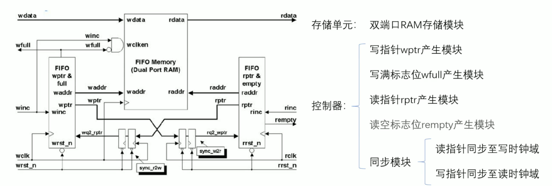
The design and implementation of asynchronous FIFO involves many key aspects, including its structure, read-write control, clock synchronization and data integrity protection. The first step in designing an asynchronous FIFO is to validate the FIFO specification, including data width, depth, and pointer width. Secondly, the structure of FIFO is designed from four parts: write controller, read controller, FIFO Memory and clock synchronization. After the structure design, the control logic of FIFO is written from three parts: empty full detection, read-write enable signal and clock domain intersection. Metastable protection and data verification in dealing with data integrity. Finally, the design of FIFO code programming and debugging optimization and integration testing.
2.2. Current design challenges for asynchronous FIFO
The current challenges of asynchronous FIFO design include how to avoid the metastable problem, how to control the empty state efficiently, how to optimize the resource utilization and design area while ensuring high reliability and high speed, and how to improve the efficiency of cross-domain data transmission.
Metastability refers to the uncertain state of circuit output at the intersection of two or more clock signals, which may lead to data errors or system instability. To solve this problem, the researchers proposed various methods, including using Gray code for pointer coding, using shift code, and adding additional bits to determine empty state more quickly and accurately.
Asynchronous FIFO needs to effectively control its internal empty state to ensure the correct transmission of data. The traditional design method is to compare the empty full mark after reading and writing the address synchronously. This method is effective, but it has large area and low working frequency [2]. In order to improve the performance, some improved design schemes are proposed, such as using weighted Gray code for pointer coding, using Gray code counter to represent read/write pointer, and using shift code.
At the same time, with the requirement of higher performance of electronic system, the design of asynchronous FIFO should consider not only how to improve the working frequency, but also how to improve the reliability. Some studies have proposed asynchronous FIFO circuits with high reliability, high speed and programmability, and introduced fault-tolerant mechanism to improve the reliability of asynchronous FIFO.
In modern integrated circuit design, resource utilization efficiency and design area are two major considerations. Some studies have reduced circuit area and increased resource utilization by improving design options, such as simplifying conventional FIFO modules by omitting "full" signal generation modules and redundant bit depths of memory, or further improving system speed and logical utilization by adopting a fully customized circuit design approach.
A key application of asynchronous FIFO is in cross clock domain data transmission. In order to improve the efficiency of data transmission, some studies based on state label are proposed.
3. Design and Implementation of Asynchronous FIFO Structure to Avoid Metastability
Metastable problem is the most important design difficulty in asynchronous FIFO. At present, Metastable problem can be avoided by using Gray Counter, Two Level Synchronizer, Address Quartering and Gate Clock. These methods not only improve the stability and reliability of FIFO, but also reduce power consumption and improve the flexibility and consistency of design.
3.1. Gray code counter
Gray code is a binary encoding method, which is characterized by the difference that there is only one bit between two adjacent code values. In asynchronous FIFO design, the use of Gray code counter as read and write address pointer encoding mode, can effectively reduce the probability of metastable state [3]. This is because the Gray code makes each time the clock comes, only 1 bit change, which provides sufficient stability time for the system, thus avoiding the generation of metastability. In addition, the stability of asynchronous FIFO is further enhanced by comparing the empty full flag generated by Gray code pointer.
The working principle of Gray code counter mainly involves its read-write control logic and empty state judgment logic. The function of Gray code counter is to update the read and write address pointer in RAM memory to realize the effective buffer and management of the data.
Specifically, the Gray code counter avoids direct jumps between adjacent states by converting binary numbers to Gray code, thereby reducing delay in the signal path. This conversion ensures that the pointer changes continuously and smoothly during read and write operations, helping to increase the working frequency of the whole module. In addition, by adding an additional bit to read and write pointers, the empty and full states of asynchronous FIFO can be determined more quickly and accurately. This method not only improves the read-write rate, but also enhances the stability and reliability of the system.
To sum up, the working principle of Gray code counter in asynchronous FIFO is to smooth the pointer updating process by Gray code conversion, and to judge the state of FIFO quickly and accurately.
3.2. Secondary synchronizer
Asynchronous FIFO is designed to solve the problem of data exchange between different clock domain systems. The primary synchronizer is responsible for transitioning read-write addresses from an asynchronous state to a synchronous state, while the secondary synchronizer further ensures that these addresses are synchronized throughout the system. This method can not only reduce the probability of metastability, but also improve the stability and reliability of the system.
In the "DSP + FPGA" architecture, DSP and FPGA are two independent clock domain systems, there are asynchronous data exchange between them. To solve this problem, using asynchronous FIFO to cache a large number of navigation message data is an effective method. Asynchronous FIFO can cache large amounts of data, ensuring that data is not lost when it is transferred between different clock domains.
In order to improve the accuracy and stability of data transmission, the concept of synchronizer is introduced. The synchronizer is implemented by cascading two-level flip-flops to synchronize transmitted data, such as carrier control word and pseudo-code control word. This design method not only ensures the accuracy of data transmission, but also improves the stability of the system.
In addition, the asynchronous FIFO design also uses a special technology to judge the empty full state to optimize the read and write operations. For example, by adding an additional bit to read and write pointers, the empty and full states of asynchronous FIFO can be determined more quickly and accurately. This design idea is helpful to improve the efficiency and performance of FIFO.
In asynchronous FIFO, the working principle of the two-level synchronizer mainly includes the use of asynchronous FIFO cache a large number of data and cascade through the two-level trigger data synchronization. The application of these technologies not only solves the problem of data exchange between different clock domain systems, but also improves the accuracy of data transmission and system stability.
3.3. Address quartile
Address quartering is achieved by dividing the address space into four equal intervals and assigning a unique control signal to each interval. The core idea of this method is to use the partition of address space to reduce the possible metastable state of read/write pointer synchronization. Specifically, when read-write addresses are in different clock domains, direct comparison of these addresses can lead to metastability, because address pointers are multibit and metastability inevitably arises during synchronization [4]. By dividing the address space into four parts, you can ensure that only one interval of addresses can be accessed at any given time, thereby reducing the probability of metastability.
3.4. Gated clock technology
The basic idea of gated clock technology is to activate the clock signal only when needed, thus reducing unnecessary clock drive and potential metastable problems.
The implementation of gated clock technology involves optimizing the power consumption and improving the efficiency of data transmission by dynamically controlling the activation state of clock signal. In a low-power asynchronous FIFO design, gated clock technology helps reduce power consumption by 80%. In addition, the dynamic power consumption of the memory can be greatly reduced by adding a gated clock circuit, such as the 8% reduction in the power consumption mentioned in one study.
By adjusting the difference between read and write hands and the phase difference between read and write hands, the gating clock technology can control the delay with high precision, which is particularly important for cross-domain data transmission.
Gray code is used as the control circuit of asynchronous FIFO pointer, which can effectively eliminate the metastable problem in multi-clock domain. The application of gated clock technology also provides more flexibility for asynchronous FIFO design. Some designs allow for the reconfiguration of FIFO flag thresholds at runtime, and this flexibility can be further enhanced with gated clock technology to accommodate different system requirements and optimize performance.
4. Design and Implementation of High Efficiency and Low Consumption Asynchronous FIFO
4.1. FIFO with arbitrarily adjustable input bit width
The design of FIFO with adjustable input bit width needs to consider the design of asynchronous interface, dynamic configuration, efficient read/write control algorithm, flexible data storage, clock synchronization, reconfigurability and modularization. By combining the existing technologies and methods, such as Gray code coding, modularization design and FPGA -based storage scheme, an efficient and reliable FIFO design with adjustable input bit width can be realized.
First of all, we can use SDRAM as a storage medium, combined with efficient read and write control algorithm to achieve the design of large capacity cache FIFO. This design can read and write data at different rates to maximize the storage capacity and high-speed access capability of SDRAM to meet the needs of mass data storage. At the same time, SOPC technology is often used to store data in Flash because of the limited on-chip memory resources in FPGA projects. FIFO is introduced to solve the problem of frequency difference between Flash and processing module, and parallel read and write strategy is used to improve the performance and flexibility of the design.
A high speed and large capacity asynchronous FIFO based on FPGA and DDR2 SDRAM is also designed. FIFO access control of DDR2 memory based on FPGA is realized by WFIFO, RFIFO and FIFO controller. This design supports parallel data reading and writing, has fixed access cycle, and can provide high access rate.
FIFO control algorithm can be divided into two parts: FIFO control algorithm and FIFO control algorithm, which effectively solves the bottleneck problem and improves the working speed and reliability.
Programmable length FIFO memory and its controller can also be used in the application without full length. Based on 2μm CMOS technology, the length of FIFO memory can be programmed to minimize data fluctuation time.
When designing FIFO for a dedicated scenario, a number of factors need to be considered, including but not limited to data transfer rate, capacity, reliability, power consumption, and support for asynchronous operations. Several approaches to designing FIFO for specific scenarios are summarized.
For high-speed data acquisition card, need to design a high-speed, large capacity and small volume of FIFO. An effective method is to combine SDRAM and FPGA to realize high-speed data transmission by using SDRAM's large storage space and FPGA's high performance. To improve the reliability and programmability of asynchronous FIFO, you can also increase the near-full warning threshold and near-empty state bits, and compare them with Gray code pointers to improve circuit reliability.
In the design and implementation of low power asynchronous FIFO, we can reduce the power dissipation of control circuit and memory unit by introducing clock gating and bit line splitting. The performance of FIFO is improved by more than 30% by defining communication protocol and overall architecture design, including storage array design, read and write control logic and air/full decision logic. In addition, the use of weighted Gray code for pointer coding and real-time global state detector for control of write/read make asynchronous FIFO much better in performance and area overhead. There are also different applications that use separate data paths with 8T-CELL SRAM and control circuits to specialize asynchronous FIFO.
With the development of integrated circuit industry, chip integration scale becomes more and more complex. Formal verification method can be used as a supplement to traditional verification methods to improve verification efficiency. Research on model verification began in the early 1980s, when Clarke, Emerson Error: Reference source not found, Queille, Siifakis Error: Reference not found, and others jointly proposed the Model checking technology. The object of validation is the mathematical abstraction of a program (or slicing), known as a model (or migration system), which uses branch timing logic CTL to describe system properties. Bryant came up with the famous OBDDs. OBDDs are data structures that can be used to express the Boolean function Error: Reference not found. When OBDDs are introduced into model checking, symbolic model checking occurs. OBDDs multiply the number of states of a verifiable system, and OBDDs enable the CTL model verification algorithm proposed by Clarke and Emerson to verify hardware systems with more than 10120 states. Some special FIFO can overcome the limitation of traditional design by improving the design of asynchronous FIFO and combining with the formal verification method of JASPER platform.
4.2. Certain scenario specific FIFO
When designing FIFO for a dedicated scenario, a number of factors need to be considered, including but not limited to data transfer rate, capacity, reliability, power consumption, and support for asynchronous operations. Several approaches to designing FIFO for specific scenarios are summarized.
For high-speed data acquisition card, need to design a high-speed, large capacity and small volume of FIFO. An effective method is to combine SDRAM and FPGA to realize high-speed data transmission by using SDRAM's large storage space and FPGA's high performance. To improve the reliability and programmability of asynchronous FIFO, you can also increase the near-full warning threshold and near-empty state bits, and compare them with Gray code pointers to improve circuit reliability [5].
In the design and implementation of low power asynchronous FIFO, we can reduce the power dissipation of control circuit and memory unit by introducing clock gating and bit line splitting [6]. The performance of FIFO is improved by more than 30% by defining communication protocol and overall architecture design, including storage array design, read and write control logic and air/full decision logic [7]. In addition, the use of weighted Gray code for pointer coding and real-time global state detector for control of write/read make asynchronous FIFO much better in performance and area overhead [8]. There are also different applications that use separate data paths with 8T-CELL SRAM and control circuits to specialize asynchronous FIFO [9].
With the development of integrated circuit industry, chip integration scale becomes more and more complex. Formal verification method can be used as a supplement to traditional verification methods to improve verification efficiency. The research on model validation techniques began in the early 1980s, Clarke, Emerson, [10] Queille, Sifakis [11], and others jointly proposed the "Model checking" technique. The object of validation is the mathematical abstraction of a program (or slicing), known as a model (or migration system), which uses branch timing logic CTL to describe system properties. Bryant came up with the famous OBDDs. OBDDs are data structures that can be used to express the Boolean function Error: Reference not found [12]. When OBDDs are introduced into model checking, symbolic model checking occurs. OBDDs multiply the number of states of a verifiable system, and OBDDs enable the CTL model verification algorithm proposed by Clarke and Emerson to verify hardware systems with more than 10120 states [13]. Some special FIFO can overcome the limitation of traditional design by improving the design of asynchronous FIFO and combining with the formal verification method of JASPER platform.
5. Conclusion
This article delves into the basic design principles of First-In First-Out, the current design challenges, and summarizes some of the unique FIFO designs that are available today.
Though the detailed analysis of asynchronous FIFO structure, read and write control, clock synchronization and data integrity protection, it provides comprehensive guidance for the design and implementation of asynchronous FIFO.
Asynchronous FIFO is a key component of cross clock domain data transmission. Many aspects should be considered in its design and implementation. Including the determination of data width, depth and pointer width, the structure design of write controller, read controller, FIFO Memory and clock synchronization, and the writing of control logic.
Secondly, aiming at the challenge of asynchronous FIFO design, this paper proposes a series of solutions. Among them, it is introduced that Gray code is an effective method to avoid metastable problem. In addition, this paper also discusses other optimization methods, such as using weighted Gray code for pointer coding, interval-based design and configurable synchronization circuit. These methods not only improve the performance and reliability of asynchronous FIFO, but also reduce power consumption and improve the flexibility and portability of the design.
To sum up, asynchronous FIFO as an indispensable data transmission component in electronic system, its design and implementation need to consider a number of aspects. By deeply understanding the basic design principle of asynchronous FIFO, adopting effective solutions and careful design optimization, we can design high performance, high reliability and low power asynchronous FIFO. At the same time, this study also provides valuable reference and hint for the future development of asynchronous FIFO.
References
[1]. Liu, Huan-Yu. Design of a read/write unit for a FIFO [J]. Microprocessor,2019,40(01):13-15.
[2]. Liu B. Design and formal verification of asynchronous FIFO [D]. National University of Defence Technology,2012.
[3]. Ren Y. Application of DDR2 SDRAM in high-end digital storage oscilloscope [D]. University of Electronic Science and Technology of China,2009.
[4]. Shi, Hua-jun. Design implementation of efficient asynchronous FIFO [D]. Hunan University,2014.
[5]. B. Niu,H.L. Zhao. Design of a highly reliable high-speed programmable asynchronous FIFO [J].Electronic Technology. Application,2019,45(07):36-39+43.DOI:10.16157/j.issn.0258-7998.183185
[6]. ZHANG Yingwu, DU Bo, YUAN Guoshun. Design and implementation of a low-power asynchronous FIFO [J]. Electronic Devices, 2007,30(3):962-964.
[7]. Wang Yi-ming. “Read and write of FIFO based on Flash.” (2009).
[8]. Changyuan Chen. “FIFO design based on verilog HDL.” Other Conferences (2023).
[9]. Abdelhafeez Saleh;GordonRoss Ann.Reconfigurable FIFO memory circuit for synchronous and asynchronous communication.Journal [J] International Journal of Circuit Theory and Applications. Volume 49 , Issue 4 . 2021. PP 938-952
[10]. C. Kern,Formal Verification In Hardware Design: A Survey,ACM Transactions on Design Automation of Electronic Sytems, 1999,4(2):123-193.
[11]. Clarke E. M,Emerson A.synthesis of synchronization skeletons for bran ching time temporallogic [J].Lecture Notes in Computer Science,981(131):52-71.
[12]. J. R. Burch, E. M. Clarke, K. L. McMillan, D. L. Dill, and L. J. Hwang Symbolic model checking:10e 20 states and beyond,1990.
[13]. J. R. Burch, E. M. Clarke, D. Long, K. L. McMillan, D. L. Dill, Symbolic Model Checking for Sequential Curcuit Verification, IEEE Transactions on Computer Aided Design of Integraded Circuits and Systems 1994(13): 401-424.
Cite this article
Wang,M. (2024). Design and implementation of asynchronous FIFO. Applied and Computational Engineering,70,215-221.
Data availability
The datasets used and/or analyzed during the current study will be available from the authors upon reasonable request.
Disclaimer/Publisher's Note
The statements, opinions and data contained in all publications are solely those of the individual author(s) and contributor(s) and not of EWA Publishing and/or the editor(s). EWA Publishing and/or the editor(s) disclaim responsibility for any injury to people or property resulting from any ideas, methods, instructions or products referred to in the content.
About volume
Volume title: Proceedings of the 2nd International Conference on Functional Materials and Civil Engineering
© 2024 by the author(s). Licensee EWA Publishing, Oxford, UK. This article is an open access article distributed under the terms and
conditions of the Creative Commons Attribution (CC BY) license. Authors who
publish this series agree to the following terms:
1. Authors retain copyright and grant the series right of first publication with the work simultaneously licensed under a Creative Commons
Attribution License that allows others to share the work with an acknowledgment of the work's authorship and initial publication in this
series.
2. Authors are able to enter into separate, additional contractual arrangements for the non-exclusive distribution of the series's published
version of the work (e.g., post it to an institutional repository or publish it in a book), with an acknowledgment of its initial
publication in this series.
3. Authors are permitted and encouraged to post their work online (e.g., in institutional repositories or on their website) prior to and
during the submission process, as it can lead to productive exchanges, as well as earlier and greater citation of published work (See
Open access policy for details).
References
[1]. Liu, Huan-Yu. Design of a read/write unit for a FIFO [J]. Microprocessor,2019,40(01):13-15.
[2]. Liu B. Design and formal verification of asynchronous FIFO [D]. National University of Defence Technology,2012.
[3]. Ren Y. Application of DDR2 SDRAM in high-end digital storage oscilloscope [D]. University of Electronic Science and Technology of China,2009.
[4]. Shi, Hua-jun. Design implementation of efficient asynchronous FIFO [D]. Hunan University,2014.
[5]. B. Niu,H.L. Zhao. Design of a highly reliable high-speed programmable asynchronous FIFO [J].Electronic Technology. Application,2019,45(07):36-39+43.DOI:10.16157/j.issn.0258-7998.183185
[6]. ZHANG Yingwu, DU Bo, YUAN Guoshun. Design and implementation of a low-power asynchronous FIFO [J]. Electronic Devices, 2007,30(3):962-964.
[7]. Wang Yi-ming. “Read and write of FIFO based on Flash.” (2009).
[8]. Changyuan Chen. “FIFO design based on verilog HDL.” Other Conferences (2023).
[9]. Abdelhafeez Saleh;GordonRoss Ann.Reconfigurable FIFO memory circuit for synchronous and asynchronous communication.Journal [J] International Journal of Circuit Theory and Applications. Volume 49 , Issue 4 . 2021. PP 938-952
[10]. C. Kern,Formal Verification In Hardware Design: A Survey,ACM Transactions on Design Automation of Electronic Sytems, 1999,4(2):123-193.
[11]. Clarke E. M,Emerson A.synthesis of synchronization skeletons for bran ching time temporallogic [J].Lecture Notes in Computer Science,981(131):52-71.
[12]. J. R. Burch, E. M. Clarke, K. L. McMillan, D. L. Dill, and L. J. Hwang Symbolic model checking:10e 20 states and beyond,1990.
[13]. J. R. Burch, E. M. Clarke, D. Long, K. L. McMillan, D. L. Dill, Symbolic Model Checking for Sequential Curcuit Verification, IEEE Transactions on Computer Aided Design of Integraded Circuits and Systems 1994(13): 401-424.