


1. Introduction
With the development of IC technology, the popularity of the Internet of Things, and the wide application of mobile devices, people's demand for higher-performance power management chips is increasing. Among them, the LDO chip, as a very important power management chip, has the ability to effectively convert high input voltage to stable low output voltage. It is also widely used in DC voltage regulator circuits.
In recent years, the development trend of electronic products has been towards higher performance and longer battery life. Therefore, the research focus of the LDO chip gradually turns to improving power efficiency and reducing static current. Improving power efficiency is critical to reducing power consumption and extending battery life. Reducing the static current reduces unnecessary energy loss during standby to improve the overall energy performance of the device.
In recent years, many scholars have focused on optimizing the design of LDO chips. The optimization design is carried out from the following three aspects. The first is to reduce the static current. The latest LDO design reduces the static current to the micro amperage level by using a subthreshold operating MOS tube and dynamic current bias technology. The second is the improvement of power suppression over PSRR. By improving the band-gap reference source and adopting a multistage error amplifier design, the suppression ability of the LDO chip to input voltage noise and power supply interference is improved. Especially in the high-frequency environment, to ensure that the output voltage is pure and stable. There is also the optimization of transient response. Scholars employ a variety of compensation and feedback techniques. Such as fast compensation circuits and enhanced feedback control systems, which make the load transient response of modern LDO chips significantly improved.
The purpose of this paper is to study the three main aspects of learning of the above scholars. Through the analysis and elaboration of these technologies. The performance of the LDO chip and the future optimization direction can be better understood. Based on the existing LDO technology, it is expected to further enhance its application potential in high-performance electronic devices. It also meets the growing market demand.
2. Basic Knowledge of LDO Chip
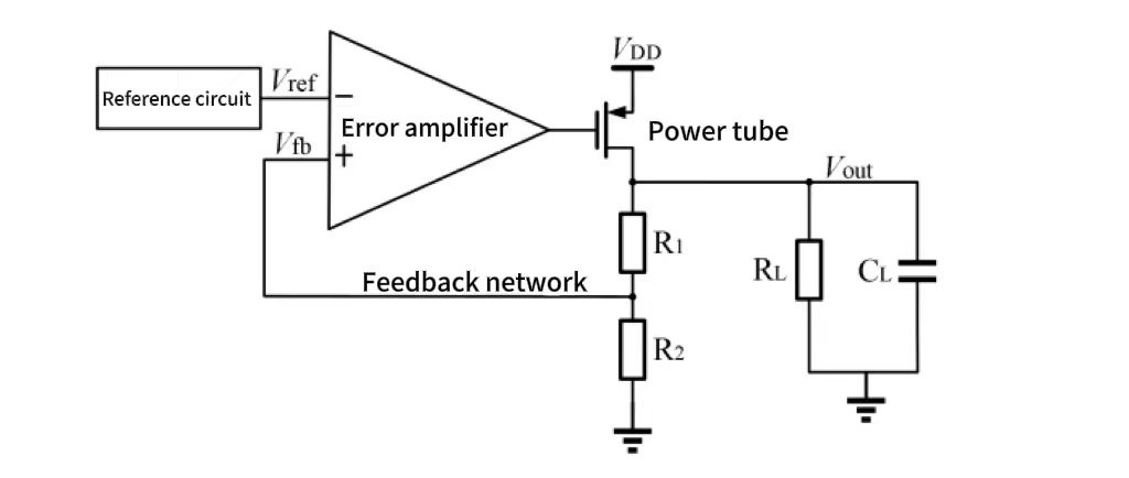
Figure 1. LDO basic structure diagram [1].
As can be seen from Figure 1, LDO can be divided into four modules. They are respectively referencing circuit module, the error amplifier module, the power tube part, and the feedback resistance network part.
2.1. Basic structure
The function of the reference circuit module is to generate a stable reference current. It is usually generated by a bandgap reference circuit. This ensures a stable reference voltage under temperature and voltage changes. At the same time, the reference voltage Vref will be supplied to the subsequent error amplifier. The output voltage of LDO is highly correlated with the reference voltage. Therefore, the stability of the reference voltage is very important for the performance of LDO chips. For the reference voltage, it will not be affected by the environment (temperature, humidity, pressure) and the power supply voltage. The reference voltage will always be maintained at a stable value [2].
For the error amplifier module, the opposite end of its input is connected to the reference voltage. The in-phase end of the input is connected with the feedback voltage after the output voltage is divided by the feedback resistance network. The error amplifier will compare the reference voltage with the feedback voltage. It can effectively detect the signal collected by the feedback network and compare the collected signal with the reference voltage. According to the results of comparison, the error between the two is amplified to generate a control signal [3]. The output voltage of the LDO is controlled by adjusting the grid voltage of the power tube and controlling its conduction, so as to produce a stable voltage value.
The power tube module is usually a PMOS or NMOS transistor. The power tube controls the transmission of input voltage to output voltage. The output voltage of the error amplifier will control the grid voltage of the power tube, and then control its conductivity. By adjusting the conduction degree of the power tube, the output voltage can be controlled very precisely [4].
For the feedback resistor module, the feedback network is composed of RFB1 and RFB2. It is responsible for feeding the output voltage back to the error amplifier in proportion to the partial voltage. The feedback network is also responsible for transmitting the feedback voltage to the input of the error amplifier. By adjusting the partial voltage ratio, the feedback network can set the target value of the output voltage.
2.2. Working principle
When the load circuit of the circuit suddenly becomes larger, the current through the sampled feedback resistance also increases. This makes the output voltage larger and the feedback voltage larger. This value is compared with the value of the reference voltage and fed into the error amplifier. The output voltage of the error amplifier increases. The increased voltage signal is transmitted to the power transistor gate. The gate-source voltage of the power tube (VGS)will decrease. From the current square law of the transistor, it can be seen that its conducting current also decreases. Finally, the output voltage decreases until it returns to a stable value [5].
Similarly, when the load current decreases, the feedback voltage will rise. The error amplifier reduces the gate-source voltage and the output current by controlling the rise of the power tube grid voltage. Keep the output voltage stable. Therefore, through this dynamic regulation mechanism, LDO can keep the output voltage constant when the supply voltage and load current change [2].
2.3. Key technology
The traditional LDO compensates for the loop by connecting a larger capacitor off-chip and using the capacitor's ESR (equivalent series resistance) to generate zero points. In this way, stable negative feedback can be achieved. However, for Ldos integrated on-chip without off-chip capacitance, the loop stability is difficult to guarantee due to the existence of multiple poles with similar frequencies. To solve this problem, researchers have proposed a variety of techniques. For example, Ka Nang Leung et al. proposed damping factor control (DFC) technology to improve the stability of LDO without off-chip capacitance [6]. In addition, Sai Kit Lau et al successfully enhanced the loop stability by reducing the Q value [7].
With the development of system-on-chip (SoC), the circuits and functions integrated on-chip are increasingly complex. The sensitivity of different modules to power supply noise increases. For example, modules such as phase-locked loops (PLL), voltage-controlled oscillators (VCO), and analog-to-digital converters (ADCs) are particularly sensitive to noise on the power supply. With the decrease of the operating voltage, the influence of the power supply fluctuation on the circuit is intensified, and the load module may even fail. To address these challenges, LDO chips need to have a higher power supply rejection ratio (PSRR). Researchers have proposed a variety of techniques to improve PSRR. Among them, the feedforward ripple cancellation technology proposed by Mohamed El-Nozahi has been widely used. On this basis, scholars continue to optimize and greatly improve the inhibition ability of LDO on power ripple [8].
In some high-speed circuit applications, such as clock generator circuits and clock refresh in memory, LDO is required to have fast transient response capability. In this way, read and write errors can be avoided [9]. To improve the transient performance of LDO, Hoi Lee et al proposed to add Slew Rate Enhancement Circuits to the LDO loop [10]. This approach significantly improves the transient response speed of LDO. In addition, Sau Siong Chong et al. further optimized the transient response performance of the LDO by introducing a push-pull buffer stage. These technologies ensure that the LDO can quickly adapt to load changes and meet the needs of high-speed circuits [11].
3. Development and Application
3.1. Current technological achievements
LDO chips play an important role in modern electronic design. With the continuous progress of technology, in order to improve the performance of LDO chips, The following aspects of improvement will be focused on.
The first is the optimization of power efficiency and static current. In recent years, the design focus of low-power LDO chips has gradually shifted to improving power efficiency and reducing static current. Static current refers to the current consumed by the LDO in the state of no load or light load. It is a key index to measure the power consumption performance of LDO, which directly affects its performance in practical applications. The static current of modern low-power LDO chips is significantly reduced under light or no load, thus extending the battery life of battery-powered devices. The low-temperature drift current of 30nA was generated by using the technology of low temperature drift bias circuit in VLSI Institute of Zhejiang University. This reduces the static operating current of the LDO to 4µA. In this way, the LDO chip can maintain a low static current without increasing power consumption. In addition, a novel dynamic Miller frequency compensation structure is designed. The zero point that can track the change of output current is introduced into Miller compensation to offset the output pole, to improve the stability of the system and make it not affected by the change of output current [12]. Although the introduction of dynamic Miller compensation technology and low-temperature drift current bias circuit improves the performance of LDO, it also increases the complexity of circuit design. This can lead to increased design difficulty and higher requirements for engineers' design and commissioning capabilities. Due to the need to achieve high-precision current bias and complex compensation circuits, the LDO design may require a higher chip area and manufacturing process.
The second is the improvement of the power supply rejection ratio (PSRR). The power supply rejection ratio (PSRR) is one of the important indexes to measure the performance of LDO. LDO chips with high PSRR can effectively suppress noise and interference in the input voltage and provide a cleaner output voltage. In recent years, the PSRR of low-power Ldos has been significantly improved through the adoption of more advanced circuit design and optimization techniques, making them superior in demanding analog and RF applications. In the study, Xu Cong et al. improved the PSRR performance of the bandgap reference source used a two-stage error amplifier to obtain higher LDO loop gain, and finally made the LDO have excellent PSRR performance at low frequency. Regardless of any temperature, process Angle, power supply voltage, or load, the PSRR can be maintained above -80 dB, which greatly improves the stability of LDO in practical applications. In addition, under the premise of taking into account the power consumption, the static working current of the LDO module excluding the bandgap reference source is less than 50 μA, and the low power consumption is realized. These improvement measures show that the overall performance of LDO can be significantly improved by optimizing the band-gap reference source and the compensation mode of LDO, especially in high-frequency and wideband noise environments [13].
LDO chips have also made significant progress in load transient response. Transient load response refers to the response speed and efficiency of a low-voltage differential linear regulator to load changes. This is an important parameter to measure power management performance. For the power management chip, the ability to quickly and stably adjust the output voltage in the sudden change of the load is the key to ensure the normal operation of the electronic equipment. Load requirements can easily change during the operation of electronic equipment. These rapid load changes, if not timely power response, may lead to equipment performance degradation and even system instability. Especially in high performance applications. Such as processors, communication equipment and precision measurement equipment, these devices require very high-power stability and response speed. In modern LDO design, a variety of compensation and feedback techniques are used to improve the stability and response speed of the chip when the load current changes rapidly. These technologies include dynamic current regulation, fast compensation circuits, and enhanced feedback control systems. Together, they act on the LDO chip to enable fast output adjustments and minimize voltage fluctuations. Fast transient response is critical. Because it ensures that when the load demand suddenly increases or decreases, the LDO chip can quickly adjust its output voltage to avoid affecting the performance or stability of the device.
In the study of He Zewei et al., it is proposed to improve the transient response capability of LDO by optimizing design and adopting advanced compensation strategies. Studies have shown that the designed LDO has a voltage drop of only 200 mV at a maximum load current of 500 mA, indicating superior transient performance. In addition, the output capacitance is 10 μF and the load current jumps at full load within 1μs. In this case,the overshoot value of the output voltage is maintained within 21 mV. The recovery time of the maximum downkick is within 15μs [13]. These performance indicators demonstrate the LDO's ability to maintain a stable output voltage when the load current changes rapidly. This is particularly suitable for high-performance analog and RF applications. It can be seen that the progress of low-power LDO chips in dynamic response and transient performance. This design not only maintains voltage stability, but also improves the speed of response to rapid load changes. This is critical to meet the high requirements for power supply stability and response speed in modern electronic devices. The development and application of these technologies have promoted the further progress of LDO technology in high-performance power management.
3.2. Application field
LDO chips are widely used in modern electronic equipment. In portable electronic devices such as smartphones, tablets, smartwatches and fitness trackers, LDO chips are used to provide a stable voltage to key components such as processors, camera modules and displays, ensuring the proper operation of the device and extending battery life. In iot devices, LDO chips provide low-noise power for sensor nodes and low-power communication modules, ensuring the accuracy of data acquisition and the high efficiency of the system.
In addition, in RF and communication equipment, LDO chips are used in network equipment such as radio transceivers and base stations to provide low-noise power to improve signal purity and system stability. In medical devices, LDO chips are widely used in portable and implantable medical devices. For example, blood glucose monitors and pacemakers provide a stable power supply to ensure the measurement accuracy and safety of the equipment.
Industrial automation and control systems also rely on LDO chips to provide low-noise power to sensors and signal conditioning circuits, ensuring signal measurement accuracy and system stability. Such as portable audio players and home sound systems. LDO chips are used to provide a stable power supply for audio amplifiers and Dacs (digital to analog converters), thereby improving sound quality and reducing the impact of power noise on audio output.
At the same time, LDO chips play a key role in battery management systems for electric vehicles and portable energy storage devices, enhancing the safety and reliability of the system by providing a stable power supply. LDO chips are also widely used in consumer electronics. Such as household appliances and smart home equipment, to provide a stable working voltage to ensure its normal operation. In general, LDO chips occupy an important position in all kinds of modern electronic devices due to their stability, low noise and low power consumption characteristics.
4. Future and Challenges
The future development of low-power LDO chips is full of opportunities and challenges. With the continuous progress of science and technology and the increasing demand for power management of electronic devices, low-power LDO chips will be widely used and improved in many emerging fields.
In terms of applications, as mentioned above, LDO chips will be widely used in emerging fields such as the Internet of Things, wearable devices (including mobile devices, etc.) and medical devices. Iot devices need to operate for long periods of time and frequently enter low-power mode. This mode of operation puts forward higher requirements for efficient power management of LDO chips. Wearable devices, such as smartwatches and fitness trackers, have extremely high battery life requirements. LDO chips will provide longer battery life for these devices. In addition, the demand for low power consumption and high precision power management in portable medical devices is also increasing. LDO chips will play an important role in these areas.
The introduction of new materials (such as wide-band gap semiconductors) and advanced processes (such as FinFET) will further improve the performance and efficiency of LDO chips. The application of intelligent power management technology will enable LDO chips to respond more flexibly to different application scenarios and further optimize power consumption. The development of system-level packaging and high integration will enable higher integration and lower power consumption.
Although LDO chips have a lot of potential, it also means that there are still many challenges in the development process. The challenge is related to the performance and properties that need to be improved in the previous article. First, further reducing the static current is a huge challenge. Especially in standby and idle modes, extremely low static current is essential to extend battery life. At present, due to the limitations of process technology, it is very difficult to maintain high performance while reducing static current. In the future, it may be necessary to introduce new materials to further optimize. Second, improving the power supply rejection ratio (PSRR) capability of LDO chips is a challenge in high-frequency and wideband noise environments. A high PSRR is particularly important for high-performance analog and RF applications, requiring fine optimization in the design. To achieve high PSRR, complex filtering and compensation networks are needed in circuit design. This step increases the design difficulty and cost and requires developers to balance complexity and suppression ratios. High PSRR puts great demands on the manufacturing process. Any small process deviation will affect its final performance, so the experimental facilities and personnel operating accuracy also put forward new requirements. Improving transient response capability is also a major challenge for LDO chips. Improving transient response requires very fast feedback loops, which requires the use of high-speed amplifiers and control circuits in the design.
At the same time, the fast transient response is easy to cause the instability of the system. Careful debugging is required in the design to prevent oscillations and overshoot. This means that under rapidly changing load conditions, LDO chips need to have fast transient response capabilities. This requires a balance between stability and speed of response in the design, ensuring a stable output voltage under a variety of operating conditions. As the power density increases, the thermal management of LDO chips becomes more complex. Effective thermal design and material selection are key to ensuring chip reliability and performance.
In short, low-power LDO chips have broad application prospects in the future, but they also face many challenges such as technology, design, and cost. Through continuous technological innovation and optimized design, it is believed that low-power LDO chips will play an important role in more fields.
5. Conclusion
LDO chip plays an important role in modern electronic design. Its development process shows remarkable technical progress and broad application prospects. The basic principles, research progress, future prospects, and challenges of low-power LDO chips are analyzed in the paper.
In recent years, LDO chips have made remarkable progress in power efficiency, static current optimization, power supply rejection ratio (PSRR), and transient response improvement. Through the use of new materials, new processes, and intelligent power management technology, low-power LDO chips perform well in a variety of high-performance applications. The integration degree and power consumption optimization of LDO chips are further improved.
However, the development of LDO chips also faces many challenges, including how to further reduce static current, improve power rejection ratio, improve transient response, effective thermal management, and control manufacturing costs. These challenges also require designers to make continuous efforts in technological innovation and design optimization at the same time.
Overall, LDO chips will continue to play an important role in various electronic devices in the future. Through continuous technological innovation and optimized design, LDO chips can not only meet the needs of existing applications but also promote the development of emerging technologies and applications to provide more complete solutions for efficient power management.
References
[1]. Liu Z F 2023 Research and Design of Fast Transient Response Off-Chip Capacitor LDO Jiangxi University of Science and Technology pp 1-75
[2]. Xiao Z 2023 Design of LDO with High Voltage and Low Power Consumption Nanjing University of Posts and Telecommunications pp 1-65
[3]. Lai B 2023 Design and Technology Research of Wide Input Low Power LDO University of Electronic Science and Technology of China pp 1-70
[4]. Hu Y 2007 Design of LDO Linear Regulator with Low Power Consumption and High Stability Huazhong University of Science and Technology pp 1-60
[5]. Yu S S 2022 Research and Design of a Fast Transient Response LDO Without Off-Chip Capacitor Xidian University pp 1-80
[6]. Leung K N Mok P K T 2003 A Capacitor-Free CMOS Low-Dropout Regulator with Damping-Factor-Control Frequency Compensation IEEE Journal of Solid-State Circuits 38(10) pp 1691-1702
[7]. Lau S K Mok P K T Leung K N 2007 A Low-Dropout Regulator for SOC with Q-Reduction IEEE Journal of Solid-State Circuits 42(3) pp 658-664
[8]. El-Nozahi M Amer A Torres J et al 2010 High PSR Low Drop-Out Regulator with Feed-Forward Ripple Cancellation Technique IEEE Journal of Solid-State Circuits 45(3) pp 565-577
[9]. Yang F Mok P K T 2017 A 65nm Inverter-Based Low-Dropout Regulator with Rail-to-Rail Regulation and Over −20dB PSR at 02V Lowest Supply Voltage 2017 IEEE International Solid-State Circuits Conference (ISSCC) San Francisco CA pp 106-107
[10]. Lee H Mok P K T Leung K N 2005 Design of Low-Power Analog Drivers Based on Slew-Rate Enhancement Circuits for CMOS Low-Dropout Regulators IEEE Transactions on Circuits and Systems II Express Briefs 52(9) pp 563-567
[11]. Chen D 2006 A LDO linear regulator with low static current and high stability Journal of Electronics & Information Technology 8 pp 1526-1529
[12]. Xu C 2012 Design of LDO with High PSRR and Low Power Consumption Fudan University
[13]. He Z 2015Design of LDO chip with fast transient response, High efficiency and high stability University of Electronic Science and Technology of China
Cite this article
Lai,J. (2024). Recent advances in LDO chip research. Applied and Computational Engineering,101,240-246.
Data availability
The datasets used and/or analyzed during the current study will be available from the authors upon reasonable request.
Disclaimer/Publisher's Note
The statements, opinions and data contained in all publications are solely those of the individual author(s) and contributor(s) and not of EWA Publishing and/or the editor(s). EWA Publishing and/or the editor(s) disclaim responsibility for any injury to people or property resulting from any ideas, methods, instructions or products referred to in the content.
About volume
Volume title: Proceedings of the 2nd International Conference on Machine Learning and Automation
© 2024 by the author(s). Licensee EWA Publishing, Oxford, UK. This article is an open access article distributed under the terms and
conditions of the Creative Commons Attribution (CC BY) license. Authors who
publish this series agree to the following terms:
1. Authors retain copyright and grant the series right of first publication with the work simultaneously licensed under a Creative Commons
Attribution License that allows others to share the work with an acknowledgment of the work's authorship and initial publication in this
series.
2. Authors are able to enter into separate, additional contractual arrangements for the non-exclusive distribution of the series's published
version of the work (e.g., post it to an institutional repository or publish it in a book), with an acknowledgment of its initial
publication in this series.
3. Authors are permitted and encouraged to post their work online (e.g., in institutional repositories or on their website) prior to and
during the submission process, as it can lead to productive exchanges, as well as earlier and greater citation of published work (See
Open access policy for details).
References
[1]. Liu Z F 2023 Research and Design of Fast Transient Response Off-Chip Capacitor LDO Jiangxi University of Science and Technology pp 1-75
[2]. Xiao Z 2023 Design of LDO with High Voltage and Low Power Consumption Nanjing University of Posts and Telecommunications pp 1-65
[3]. Lai B 2023 Design and Technology Research of Wide Input Low Power LDO University of Electronic Science and Technology of China pp 1-70
[4]. Hu Y 2007 Design of LDO Linear Regulator with Low Power Consumption and High Stability Huazhong University of Science and Technology pp 1-60
[5]. Yu S S 2022 Research and Design of a Fast Transient Response LDO Without Off-Chip Capacitor Xidian University pp 1-80
[6]. Leung K N Mok P K T 2003 A Capacitor-Free CMOS Low-Dropout Regulator with Damping-Factor-Control Frequency Compensation IEEE Journal of Solid-State Circuits 38(10) pp 1691-1702
[7]. Lau S K Mok P K T Leung K N 2007 A Low-Dropout Regulator for SOC with Q-Reduction IEEE Journal of Solid-State Circuits 42(3) pp 658-664
[8]. El-Nozahi M Amer A Torres J et al 2010 High PSR Low Drop-Out Regulator with Feed-Forward Ripple Cancellation Technique IEEE Journal of Solid-State Circuits 45(3) pp 565-577
[9]. Yang F Mok P K T 2017 A 65nm Inverter-Based Low-Dropout Regulator with Rail-to-Rail Regulation and Over −20dB PSR at 02V Lowest Supply Voltage 2017 IEEE International Solid-State Circuits Conference (ISSCC) San Francisco CA pp 106-107
[10]. Lee H Mok P K T Leung K N 2005 Design of Low-Power Analog Drivers Based on Slew-Rate Enhancement Circuits for CMOS Low-Dropout Regulators IEEE Transactions on Circuits and Systems II Express Briefs 52(9) pp 563-567
[11]. Chen D 2006 A LDO linear regulator with low static current and high stability Journal of Electronics & Information Technology 8 pp 1526-1529
[12]. Xu C 2012 Design of LDO with High PSRR and Low Power Consumption Fudan University
[13]. He Z 2015Design of LDO chip with fast transient response, High efficiency and high stability University of Electronic Science and Technology of China