


1. Introduction
The advent of computer technology has enabled the simulation of hardware design on software, which mainly involves two types of design software, Computer Aided Design (CAD) and Electronic Design Automation (EDA). Based on the CAD technology, the EDA is used for designing semiconductor IC. After a long period of development, it is now one of the most important areas in the field of electrical engineering. The machine learning is an important part of artificial intelligence. It simulates the process of human’s studying, which becomes a trend in the future. (The development of the machine learning method (ML method) affects other computer- related domains. By the development of the computer technology, the algorithms of EDA had made some progress. However, the function of EDA was relatively limited. Consequently, there) There was a concern about the future development of EDA when it compares with machine learning [1]. In recent years, “ML for EDA” has emerged [2], namely the use of ML methods to enhance and modernize the functionality of EDA tools. The paper aims to examine the evolution of EDA and its integration with ML, as well as to identify potential future trends in EDA. The advent of ML for EDA has opened new avenues for the advancement of EDA. However, this approach still encounters significant obstacles. Therefore, it provides an overview of EDA, an analysis of the application of ML to solve EDA problems, and an examination of the challenges facing ML-based EDA. Additionally, potential solutions to these challenges are presented. By synthesizing and elucidating the findings of the extant literature, this paper offers a comprehensive account of EDA, delineates the most efficacious ML approaches for EDA in recent studies, and analyzes their prospective trajectories to provide an objective account of the evolution of EDA and the challenges it confronts. This will undoubtedly prove invaluable in facilitating the future development of EDA, particularly in the context of ML-based EDA.
2. Overview of Electronic Design Automation
2.1. Definition and Concept
EDA is a type of automated software utilized for the design of ICs, especially VLSIs, which is also called ECAD by the reason of being a type of computer aided design (CAD). It is an excellent tool for engineering and academia to assist in the specification, simulation, design, verification, and testing of electronic systems and circuits [1]. In the mid-1970s, EDA was developed in that the design and testing of integrated circuits was too complex for humans. Throughout the evolution of EDA, the software has been constantly updated, incorporating new features that facilitate its use and enhance its capabilities. In recent times, most of the billion-transistor chips used in modern computers and smart devices have been designed by EDA. As shown in Figure 1, EDA has two main components, namely front-end design and back-end design. Front-end design implements the functionality of the integrated circuit, while back-end design transforms the circuit into a physical panel [3]. Each step of the design process is supported by complex algorithms. For example, the Boolean Satisfiability Algorithm (SAT) is often used for automated test pattern generation for EDA [4], a key stage in back-end design.
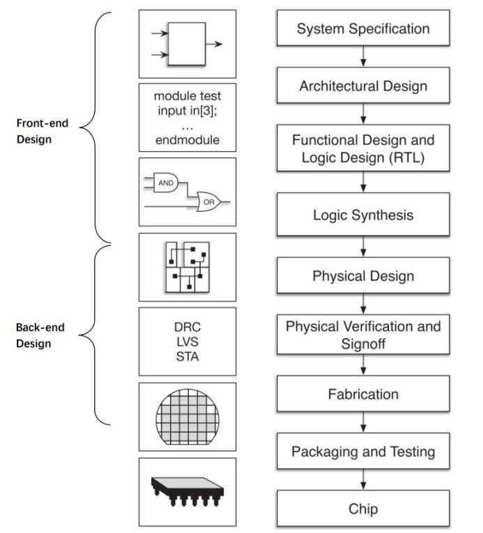
Figure 1. Modern Chip Design Flow [2]
2.2. Development Milestones
Prior to the 1960s, Shannon's work on Boolean algebra and McCluskey’s work on minimization of combinational logic circuits formed the theoretical basis of EDA [5]. The prototype of EDA was then developed in the late 1960s on the basis of CAD. Previously, most of the circuit designs was done manually. From 1964 to 1978, a large amount of pioneering work laid the foundation for EDA. These achievements can be divided into five parts: circuit simulation, logic simulation and testing, MOS timing simulation, wire routing and regular arrays [6]. In this period, EDA was gradually separated from CAD and became an independent designing software. EDA began to grow rapidly from 1979 to 1993, during which time more and more people attended EDA forums and exhibitions, and experts and students in the field of EDA were widely invited to refine its capabilities. From 1979 to 1981, there was a notable surge in the number of papers on EDA. At that time there were six achievements: verification and testing, layout, logic synthesis, hardware description languages, hardware acceleration and high-level design [6]. In addition, the EDA field began to expand into artificial intelligence during this period. After 1993, EDA entered a new era in which it became more mature than ever before. Furthermore, system on chip (SoC) has attracted the attention of the professionals. However, the pace of technological innovation began to slow down. In this time, there appeared a concern about EDA’s future trend by this reason. Recently, a new opportunity has emerged in EDA to use ML methods to optimize the complexity and data availability of the IC design process [7]. Research in this field has been ongoing for approximately a decade and is anticipated to yield results in the near future.
2.3. Key Technologies and Major Challenges
Various key technologies provide the foundation for the EDA capabilities, including virtual prototype verification, logic synthesis, physical synthesis, circuit simulation analysis, and layout design.
Virtual prototyping is the evaluation of integrated circuits on a computer using virtual prototyping techniques, usually used in the physical verification step. During the circuit design process in EDA, the computer should build the circuit in a virtual prototype. After that, the system will simulate the prototype on FPGA to accelerate the simulation of gate level and register transfer level (RTL) [8]. Logical synthesis is used for analyzing the function of IC, representing a crucial stage in the front-end design phase. This involves the conversion of behavioral-level descriptions into gate-level descriptions, which is a particularly significant aspect within the field of EDA [2]. A variety of algorithms are used in the construction of gate circuits, such as SAT algorithms which realizes simple gate circuits by performing operations on CNF formulas [4]. Physical synthesis represents a pivotal aspect of back-end design, comprising two principal phases, namely physical design and physical verification. Physical design can be further categorized into steps such as layout planning, layout, clock tree synthesis and wiring [9], which is responsible for mapping the circuit netlist onto the physical layout and ensuring the robustness of the manufacturing process. Circuit simulation is used to evaluate designed integrated circuits on a computer, also known as computer-aided circuit analysis, which is often used in back-end design to test that the circuit is correct and implements the desired function. This technique is based on complex algorithms on a computer and is faster and more accurate than traditional breadboard testing. Wiring design is the translation of conceptual circuits into physical circuits and helps design how electronic components will be mounted on a printed circuit board (PCB). It is usually used in the final stage of back-end design. Once this process is completed, the circuit can be fabricated in the real world.
Nevertheless, there are also challenges to the development of EDA. First, integrated circuits are being designed on an increasingly large scale [9]. Even with a modular design approach, back-end design software still needs to handle circuit modules with logic gate scales ranging from millions to tens of millions, which poses significant challenges to the efficiency of algorithms in various back-end design steps. Moreover, the design goals and constraints of EDA are becoming increasingly intricate. Introducing more complex design rules and device/interconnect models into advanced technologies not only significantly increases the difficulty of generating rational layouts, but also increases the cost of performance evaluation. In addition, the design process is likely to require a greater investment of time than was previously the case. The protracted back-end design process and the high degree of coupling between each step result in inefficient iterations and a slow rate of design convergence. Finally, with the development of AI, there is a need for more advanced and smarter EDAs, as the demand for EDAs is increasing, especially after the COVID-19 pandemic [10].
3. Application of Machine Learning in Electronic Design Automation
To address these challenges of EDA development, a new perspective is proposed to improve EDA through ML methods, which covers almost all phases of the chip design flow. In recent times, machine learning techniques have undergone a period of rapid evolution, providing excellent modeling and search performance in many areas, such as image recognition. Recently, there has been a proliferation of machine-learning-based ML methods, which can be categorized into a variety of types, as shown in Figure 2. The use of machine learning is becoming increasingly prevalent in optimization, so as to enhance the performance and efficiency of traditional algorithms in other domains. The use of ML methods presents a potential solution to the challenges currently faced by EDA.
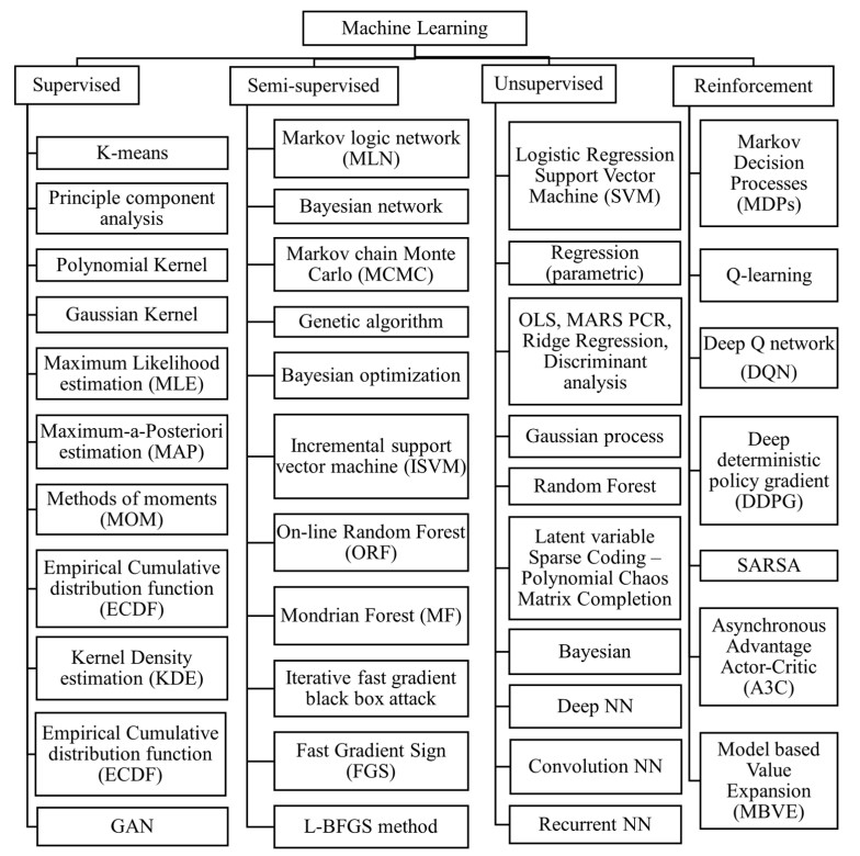
Figure 2. Classification of ML Methods [7]
The prevailing perspective on the application of machine learning in EDA is the utilization of ML techniques to enhance the functionality of physical design processes, which encompass clock tree synthesis (CTS), floor planning, and layout routing (or layout).
3.1. Clock trees synthesis (CTS)
In digital integrated circuit design, the clock signal is the reference for data transmission. Notably, the clock signal plays a decisive role in the functionality, performance, and stability of synchronous digital systems. Consequently, in standard cell-based ASIC processes, CTS is the key step of back-end design to implement the clock network. However, traditional CTS leads to increased currents at the edge of the clock activity. To mitigate the impact of peak currents, a comprehensive, automated solution is employed, leveraging the capabilities of reinforcement learning, a machine learning technique. The system assists in modifying the clock arrival time of each register, thereby optimizing the distribution of clock arrivals [7]. In addition, generative adversarial network (GAN), an ML method, can help in clock tree prediction. Artificial Neural Networks (ANN) are used to support GAN. CTS with GAN, which is also known as GAN-CTS [9], optimizes the clock tree by estimating the elements of the clock tree using conditional generative adversarial networks. This method is effective in reducing energy consumption and exploring better clock trees.
3.2. Floor planning and Placement
Even though these two processes represent disparate stages in the back-end design of the chip design flow, they are similar in principle and both are important parts of the design flow. Additionally, they are regarded as one of the most time-consuming and complex process, built from highly sophisticated algorithms. The major responsibility of the stages is to locate logic blocks within the IC in accordance with field-programmable gate arrays (FPGA) architecture [11]. Modern chip designs require multiple iterations of localization to ascertain the same location for each component [7], thereby creating an opportunity for the application of ML methods. Consequently, the combination of ML methods with traditional algorithms represents a promising avenue of research. To this end, an expert trains the model, which is a learning-based approach that is capable of learning from previous experiences and gradually self-updating the method. This approach also constitutes an RL-based solution, which utilizes an RL-based graph placement method. In this case, better performance can be obtained while maintaining the robustness of traditional algorithms.
3.3. Routing
In the final stage of the back-end design, EDA connects the components of an IC together, which is called routing. It is well known that individual circuits have a large number of routing possibilities. However, there is a requirement for routing, i.e. total wirelength. To fulfill the routing requirement, design role checking (DRC) is employed for the error detection. A CNN called RouteNet is applied to DRC, but a RouteNet is insufficient for the research purposes, routing information prediction is also required, which is supported by a customized Fully Convolutional Network (FCN). Besides, an 18-layer ResNet is used to predict design rule violation (DRV) count [2]. With the help of ML method, better routing approaches can be discovered more rapidly and accurately. In addition to physical design, studies have pointed out that ML method can be employed in other domains of EDA. For example, lithography simulation and mask synthesis [9] can be improved by ML method, and CNN or GNN models can navigate circuit design (front-end design) [12]. These ML methods may improve the efficiency of EDA.
4. Future Development Trends
The application of ML methods to CAD, including EDA, is a highly active area of research. However, there is still many challenges. Firstly, there are virtually no ML public datasets dedicated to CAD (or EDA) applications due to licensing constraints and specific domain expertise in generating the data [3]. “ML for EDA” merges two different domains into one, which did not cooperate before. In addition, the time for it is not adequate. That illustrates it is still at the early stage of “ML for EDA”. Moreover, the existing datasets obtained from CAD (or EDA) contests are often incomplete and not designed for ML applications [3]. EDA and CAD have been around for a long time, during which time engineers working in the field did not begin to focus on machine learning until approximately a decade ago. At present, EDA is highly mature, and its dataset is exceptionally complex due to the complexity of hardware electronic components’ dataset, i.e. component parameters, functions and simulation effect under different conditions, which is really hard for recent ML method to manage. Moreover, there are a number of possible future solutions to these challenges. The constraints imposed by licensing restrictions and the need for domain-specific expertise in data generation may be overcome with the passage of time. The key challenge lies in the intrinsic nature of the dataset. In the case of complex datasets for EDA (e.g., electronic component libraries), the necessity arises for the creation of a novel data structure to facilitate machine learning. Concurrently, the algorithms utilized in machine learning have undergone further advancement. Consequently, the data structure will be applicable to both domains. It is anticipated that in the future, machine learning will be more seamlessly integrated with traditional algorithms designed for digital back-ends.
5. Conclusion
As a specialized CAD, EDA is a useful tool in both engineering and academic, which has developed for a long period. In the period, this period, a lot of research and experiments have been carried out on it, and the algorithms of EDA have been gradually updated and improved. Despite the considerable advancement of EDA technology and its enhanced capabilities, there are indications that EDA is facing challenges, particularly in the context of the ongoing pandemic, which has led to an increase in demand for integrated circuit products. Compared to other areas of computer science (i.e., machine learning), the development of EDA is worrisome. Therefore, a new type of EDA is proposed, i.e., machine learning-based electronic design automation, which is the improvement of functions or algorithms in EDA by employing ML methods. The rapid advancement of machine learning may drive new leaps forward in the progress of EDA. Recent studies have demonstrated that machine learning can enhance nearly every stage of the EDA chip design process. However, the majority of studies concur that ML methodologies can facilitate updates to the physical design of EDA. Furthermore, there are several obstacles or difficulties associated with ML-based EDA, particularly in the context of complex datasets characteristic of older EDAs. To address these challenges, research in the field of electronic design automation (EDA) needs to invest more time and effort.
References
[1]. Curiac, C.D. and Doboli, A. (2022) Combining informetrics and trend analysis to understand past and current directions in electronic design automation. Scientometrics, 127: 5661–5689.
[2]. Huang, G.Y., Hu, J.B., et al. (2021) Machine Learning for Electronic Design Automation: A Survey. ACM Trans. Des. Autom. Electron. Syst. 26(5), 1-46.
[3]. Chai Z.M., Zhao Y.X., et al. (2022) CircuitNet: an open-source dataset for machine learning applications in electronic design automation (EDA). Sci China Inf Sci, 65(12): 227401.
[4]. Marques-Silva, J.P. and Sakallah, K.A. (2000) Boolean satisfiability in electronic design automation. Proceedings of the 37th Annual Design Automation Conference, 675-680.
[5]. MacMillen, D., et al. (2000) An industrial view of electronic design automation. IEEE transactions on computer-aided design of integrated circuits and systems, 19(12): 1428-1448.
[6]. Sangiovanni-Vincentelli, A.L. (2003) The tides of EDA. IEEE Design & Test of Computers, 20(6): 59-75.
[7]. Gubbi, K.I., et al. (2022) Survey of Machine Learning for Electronic Design Automation. GLSVLSI’22: Proceedings of the Great Lakes Symposium on VLSI 2022, 513-518.
[8]. Oetjens, J-H., et al. (2014) Safety evaluation of automotive electronics using virtual prototypes: State of the art and research challenges. Proceedings of the 51st annual design automation conference,1-6.
[9]. Lin, Y.B., Gao, X.H., et al. (2021) Machine learning assisted backend design method for digital integrated circuits. Micro/nano Electronics and Intelligent Manufacturing, 3(2): 11-20.
[10]. Marinova, G.I., et al. (2021) Challenges and opportunities for semiconductor and electronic design automation industry in post-Covid-19 years. IOP Conference Series: Materials Science and Engineering, 1208(1): 1-6.
[11]. Hamolia, V. and Melnyk, V. (2021) A Survey of Machine Learning Methods and Applications in Electronic Design Automation. 2021 11th International conference on advanced computer information technologies (ACIT), 757-760.
[12]. Chen, T.H., et al. (2022) Machine learning in advanced IC design: A methodological survey. IEEE Design & Test, 40(1): 17-33.
Cite this article
Li,J. (2024). A study of advances in machine learning-based electronic design automation. Applied and Computational Engineering,102,96-101.
Data availability
The datasets used and/or analyzed during the current study will be available from the authors upon reasonable request.
Disclaimer/Publisher's Note
The statements, opinions and data contained in all publications are solely those of the individual author(s) and contributor(s) and not of EWA Publishing and/or the editor(s). EWA Publishing and/or the editor(s) disclaim responsibility for any injury to people or property resulting from any ideas, methods, instructions or products referred to in the content.
About volume
Volume title: Proceedings of the 2nd International Conference on Machine Learning and Automation
© 2024 by the author(s). Licensee EWA Publishing, Oxford, UK. This article is an open access article distributed under the terms and
conditions of the Creative Commons Attribution (CC BY) license. Authors who
publish this series agree to the following terms:
1. Authors retain copyright and grant the series right of first publication with the work simultaneously licensed under a Creative Commons
Attribution License that allows others to share the work with an acknowledgment of the work's authorship and initial publication in this
series.
2. Authors are able to enter into separate, additional contractual arrangements for the non-exclusive distribution of the series's published
version of the work (e.g., post it to an institutional repository or publish it in a book), with an acknowledgment of its initial
publication in this series.
3. Authors are permitted and encouraged to post their work online (e.g., in institutional repositories or on their website) prior to and
during the submission process, as it can lead to productive exchanges, as well as earlier and greater citation of published work (See
Open access policy for details).
References
[1]. Curiac, C.D. and Doboli, A. (2022) Combining informetrics and trend analysis to understand past and current directions in electronic design automation. Scientometrics, 127: 5661–5689.
[2]. Huang, G.Y., Hu, J.B., et al. (2021) Machine Learning for Electronic Design Automation: A Survey. ACM Trans. Des. Autom. Electron. Syst. 26(5), 1-46.
[3]. Chai Z.M., Zhao Y.X., et al. (2022) CircuitNet: an open-source dataset for machine learning applications in electronic design automation (EDA). Sci China Inf Sci, 65(12): 227401.
[4]. Marques-Silva, J.P. and Sakallah, K.A. (2000) Boolean satisfiability in electronic design automation. Proceedings of the 37th Annual Design Automation Conference, 675-680.
[5]. MacMillen, D., et al. (2000) An industrial view of electronic design automation. IEEE transactions on computer-aided design of integrated circuits and systems, 19(12): 1428-1448.
[6]. Sangiovanni-Vincentelli, A.L. (2003) The tides of EDA. IEEE Design & Test of Computers, 20(6): 59-75.
[7]. Gubbi, K.I., et al. (2022) Survey of Machine Learning for Electronic Design Automation. GLSVLSI’22: Proceedings of the Great Lakes Symposium on VLSI 2022, 513-518.
[8]. Oetjens, J-H., et al. (2014) Safety evaluation of automotive electronics using virtual prototypes: State of the art and research challenges. Proceedings of the 51st annual design automation conference,1-6.
[9]. Lin, Y.B., Gao, X.H., et al. (2021) Machine learning assisted backend design method for digital integrated circuits. Micro/nano Electronics and Intelligent Manufacturing, 3(2): 11-20.
[10]. Marinova, G.I., et al. (2021) Challenges and opportunities for semiconductor and electronic design automation industry in post-Covid-19 years. IOP Conference Series: Materials Science and Engineering, 1208(1): 1-6.
[11]. Hamolia, V. and Melnyk, V. (2021) A Survey of Machine Learning Methods and Applications in Electronic Design Automation. 2021 11th International conference on advanced computer information technologies (ACIT), 757-760.
[12]. Chen, T.H., et al. (2022) Machine learning in advanced IC design: A methodological survey. IEEE Design & Test, 40(1): 17-33.