


1. Introduction
Low-Dropout regular (LDO) is the most important type of power management chip. LDO quickly adjusts output impedance and stabilizes output voltage according to load changes, providing low-noise power supply voltage and bias voltage for other circuit modules. At the same time, LDO has the advantages of low power consumption, simple structure, and few peripheral circuits, which is widely used in medical, communication equipment, portable electronic products and other fields [1]. Realizing high-performance LDO regulators has been the focus of several investigations in the past few years. For example, in order to meet the requirements of modern electronic devices for fast power response, static current recovery and active clamping control architecture designs have been developed; with the continuous improvement of integration and process, LDO regulators are gradually integrated into SoC chips, and LDO without external capacitors has gradually replaced LDO with external capacitors and become a research focus. Additionally, in order to fulfill the demands of applications like RF amplifiers, clocks, and timing integrated circuits, researchers are working to produce LDO regulators having a low output noise level and a good power supply rejection ratio.
This is due to the growing need for high-precision and low-noise power supplies.
There are two types of LDO: bipolar and CMOS. Generally speaking, bipolar chips can operate at higher operating voltages, have higher transconductance, and are easy to design. The best feature of CMOS is that its input requires only a very small bias current.[2] LDO has a low voltage difference as a low voltage dropout regulator. For battery-operated devices, its ability to maintain a constant output voltage even in the presence of near input and output voltages is particularly useful. Second, linear differential operators (LDOs) are simpler to create and implement than switching regulators, which are often more complex. Because of their linear characteristics, LDOs generate less noise than other types of regulators. They can thus be applied in noise-sensitive fields including radio frequency communications and precise machinery. The low quiescent current of many LDO regulators contributes to the longer lifespan of battery-operated electronics.
This article will summarize some of the main parameters of LDO chip research, and then introduce the current design of different types of LDO chips and the application of LDO chips. Finally, the development and challenges of LDO chips are summarized.
2. LDO Chip Parameters
Figure 1 depicts the usual LDO circuit configuration including error amplifier, resistor feedback network, reference voltage, and adjustment tube. These are the four essential components of the construction. When the reference voltage source is functioning normally, a precise reference voltage is generated and supplied into the error amplifier's non-inverting terminal. The feedback voltage, which is produced by dividing the output voltage by the sampling series resistor, is applied to the error comparator's inverting terminal. The error amplifier's output directly drives the adjustment element and modifies the regulator's output voltage by increasing the difference between the reference and feedback voltages and altering the adjustment element's conduction. When the feedback voltage is less than the reference voltage, the output of the error amplifier controls the adjustment element to make it flow a larger current, and the output voltage rises, and vice versa [2].
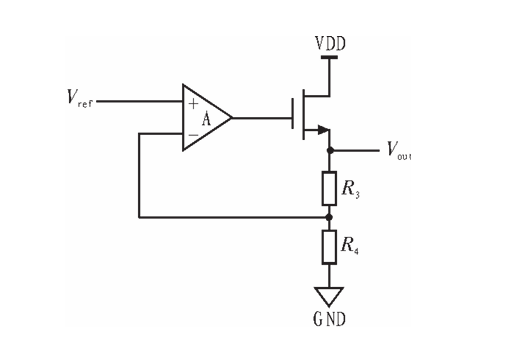
Figure 1. Typical LDO Circuit [2].
2.1. Voltage drop
A low-dropout linear regulator's typical feature is its voltage drop. Voltage drop is defined as the smallest change between the input and output voltages, or Vin and Vout, under normal management. When the input voltage falls even more and the LDO is unable to regulate, the input-to-output voltage difference (VDROPOUT) is a more realistic representation of the voltage drop. The pass element functions as a resistor in the voltage drop zone, with a resistance equal to the on-resistance from the drain to the source. The LDO design of LDO chips is the primary factor influencing voltage drop [3].
2.2. Quiescent current and ground current
"A state or phase of inactivity or dormancy" is the definition of quiescent [3]. The quiescent current (IQ) of the LDO is hence the current required to power its internal circuitry when the external load current is zero. It includes circuits for overcurrent and overtemperature detection, as well as the operating currents of the output voltage divider, error amplifier, and bandgap reference. Quiescent current is influenced by topology, temperature, and input voltage. Quiescent current is invariably present in the ground current (IGND), which is the difference between the input and output currents. LDO efficiency is maximized by low ground current [4].
2.3. Power supply rejection ratio(PSRR)
The power supply rejection ratio (PSRR) is a common specification listed in many LDO data sheets. It specifies how well an AC component of a specific frequency is attenuated from the LDO input to the output [3]. The power supply rejection ratio is a crucial performance measure for low dropout regulators (PSRR). The LDO's capacity to reduce the output voltage ripple brought on by variations in the input voltage is measured by PSRR. PSRR is enhanced by large output capacitors with low equivalent series resistance (ESR) values as well as bypass capacitors. Achieving good PSRR becomes more difficult when the load capacitors are reduced in size. Several design approaches have been put forth by researchers to implement CL-LDOs. To stabilize their regulators, most designs make use of the ideas of pole splitting and Miller capacitance. The PSRR gauges a circuit's capacity to remove unwanted signals (noise and ripple) at the power supply input before they contaminate the circuit output [5]. PSRR is dependent on frequency, thus it cannot be defined by a single value. LDO is made by a power regulation component like BJT or MOSFET, besides, voltage reference and error amplifier. The output voltage is regulated by the DC gain provided by the error amplifier. The PSRR is mostly determined by the error amplifier's ac gain characteristics. A typical LDO can have a PSRR as high as 80 dB at 10 Hz, but this drops to only 20 dB at tens of kHz [4].
2.4. Noise
There are two broad types of noise sources that can be found in any circuit, including low dropout (LDO) regulators: extrinsic and intrinsic. Intrinsic noise, as it relates to electrical circuits, is the noise produced inside any electronic device, whereas extrinsic noise comes from outside sources. The error amplifier establishes the LDO's PSRR and, consequently, its ability to reject input noise, because inherent noise always manifests itself at the LDO's output [6].
A constant output current and ripple-free input voltage across a predetermined frequency range (often 10 Hz or 100 Hz to 100 kHz) provide an output noise voltage that is the root mean square output noise voltage. The internal reference and the error amplifier in an LDO are the primary sources of output noise. In order to achieve 15 μA, modern LDOs run with internal bias currents of tens of nanoamps. There are methods that may be used to make sure that the LDO has the lowest noise characteristics in addition to choosing one with low noise characteristics. Both feed-forward and noise-reduction capacitors are used in these methods. [4]
2.5. Capacitance and capacitor
A capacitor is a charge-storage device made up of one or more conductor pairs divided by an insulator.
In order for LDO to work properly, it needs to be equipped with an output capacitor. Currently, LDO without external capacitors has become a research hotspot. The difficulty in designing LDO without external capacitors lies in how to improve system stability and transient characteristics [3].
Polarization can occasionally occur spontaneously without the requirement for an external electric field because capacitors are dynamic devices that store and release charge in nonlinear ways. We call this phenomena "spontaneous polarization." Spontaneous polarization is caused by the inert electric field of the substance that provides the initial capacitance of the capacitor. An electric field is produced when an external DC voltage is given to the capacitor. This electric field polarizes the remaining active dipoles in the opposite direction first, then "locks" them into position. Polarization and the direction of the electric field within the dielectric are related.
With bigger case sizes, there is less dielectric between the conductors, which lowers the electric field strength and the number of locked dipoles, so there is less capacitance loss.
3. Design and Application of LDO Chips
3.1. External capacitor-less LDO design
In traditional LDO chips, adding the external capacitors at the output end seems inevitable in order to improve load transient response and stability, but this often increases design costs and PCB board area, and is not compatible with the mainstream development trend of large-scale integrated circuits, the system on chip (SOC). Therefore, LDO without external capacitors has become a hot topic of research. The design of LDO without external capacitors must solve the problems of stability and enhanced transient characteristics. In terms of improving transient response, the literature has proposed several methods, such as dual-loop control. However, the problem with the dual-loop control method is that it increases the difficulty of circuit design and introduces the problem of loop frequency compensation. In addition to the dual-loop control method, there is also a zero-pole dynamic compensation method, but the loop stability is poor in extreme cases [5].
At present, many scholars have also studied the design of LDO without external capacitors. For example, a servo amplifier and a capacitor COS are used to provide a DC operating point for the gate of the power tube. The servo amplifier output stage adopts a push-pull structure. In steady state, the charge pump only needs to provide a small amount of current. Therefore, a small current charge pump design is used internally, which is easy to integrate on chip. In addition, the variable reference circuit widens the output swing of the error amplifier and enhances the transient response performance of the LDO. [5]
3.2. Bandgap reference LDO design
The goal of creating a reference is to create a DC voltage or current with a certain temperature characteristic that is unaffected by the process and power source. In order to accomplish temperature compensation, the bandgap reference source's basic working concept is to cause the negative and positive temperature coefficients to cancel each other out [2].
The entire implementation circuit of the bandgap reference voltage consists of a startup circuit and a Brokaw structure bandgap reference. For the reference voltage source circuit, startup is also an issue that needs to be considered. When the power supply is turned on, all transistors transmit zero current. Because the two branches of the circuit allow zero current, the transistor may be in an indefinite off state. At this time, it is necessary to add a circuit to get rid of this state. The startup circuit is to enable the circuit to get out of the zero current point during the power-on process and work stably; in addition, in order to reduce power consumption, the startup circuit should be disconnected after the system is working normally. The structure is shown in the figure 2 [2].
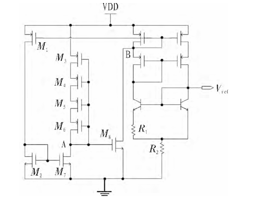
Figure 2. Bandgap Reference Practical Circuit[2].
3.3. High PSRR LDO design
In addition, the loop bandwidth of the traditional low dropout regulator (LDO) is narrow, which is not conducive to suppressing high-frequency noise, resulting in a low output power supply rejection ratio [1]. In recent years, methods such as using N-type MOS (Metal Oxide Semiconductor) transistors as power tubes and adopting cascade power tube structures have been proposed to improve the power supply rejection ratio of LDO. However, while suppressing power supply noise, the above technologies have the common problems of increasing the input-output voltage difference of LDO and limited improvement of power supply rejection ratio within the target frequency band. Cascode amplifiers can achieve larger gain and significantly reduce the Miller effect. The frequency response of this amplifier is better than that of other amplifiers. The PSRR and DC gain of the folded cascode structure are both high. High PSRR may be attained by the folded cascode structure of PMOS input transistors because the folded cascode operational amplifier using PMOS input transistors has less flicker noise than the folded cascode operational amplifier using NMOS input transistors. This advantage also makes this PMOS amplifier the main choice for LDO [8].
3.4. Low quiescent current LDO design
For wide-input electronic devices such as electric vehicles, electronic scales, and instruments, battery life is a very important indicator, so to extend the life of the battery, the circuit's quiescent current must be decreased. LDO is in a low-load state most of the time, so reducing the quiescent current under light load can achieve longer battery life. However, low quiescent current will cause the tail current of the error amplifier to decrease, thereby reducing the slew rate of the amplifier. When the load changes suddenly, the transient response characteristics of the LDO will deteriorate because the loop cannot adjust the gate voltage of the power tube in time. The low quiescent current LDO can achieve fast transient response of the LDO by adding a push-pull buffer between the error amplifier and the power tube to increase the slew rate of the gate terminal of the power tube, but the quiescent current will increase. Furthermore, the comparator and latch are employed to accomplish the LDO's quick transient response and low power consumption, although the overshoot voltage is significant. Second, low quiescent current is achieved by combining the bandgap reference and error amplifier, yet this method has a poor load capacity. In addition to the above methods, the quiescent current under no-load conditions is reduced through the low-power bandgap reference circuit and the dynamic current bias circuit. Meanwhile a transient enhancement circuit is designed to resolve the contradiction between low quiescent current and transient response. In addition, pseudo-ESR compensation, zero point compensation and other compensation methods are used to ensure that the LDO can work stably within the full load range, so that the LDO design with low quiescent current can be realized.
3.5. Low noise LDO design
One of the most important functions of the LDO is its sensitivity to power supply noise in terms of voltage generation. The classic LDO's big output capacitor can boost loop stability and PSRR, but it also expands the printed circuit board's surface area. As a result, an output capacitor-less LDO, also known as an OCL-LDO, was created. Utilizing a double-buffered OCL-LDO technology can solve the aforementioned issues. The suggested design incorporates a pre-amplifier stage structure to lower the noise of the EA and only reuses the buffer stage to achieve minimal power supply ripple and high load current without the need for huge resistors and capacitors [6].
Modern mobile devices emphasize multi-functional large-scale integration and fast operating speed, which makes the internal modules more and more power-consuming, and their dynamic current curves often contain fast-changing components, which puts strict requirements on the load capacity of the LDO and the overshoot and undershoot generated during load transients. Al-Shyouke et al. increased the slew rate of the gate terminal of the power tube by adding an adaptive bias voltage buffer between the error amplifier and the power tube, thereby enhancing the transient response. Maity et al. used adaptive bias technology for the error amplifier to increase the loop bandwidth under heavy load to improve transient response. The above method is effective when the load current is less than 100 mA, but its effectiveness may decrease when the load current increases. Therefore, a non-chip capacitor NMOS LDO for portable devices can be proposed. The power tube gate is connected in series with a large capacitance capacitor to form a floating gate structure, and the capacitor is charged and discharged by the auxiliary operational amplifier to provide a DC operating point for the power tube gate. The auxiliary operational amplifier adopts push-pull output, and the charge pump is required to provide a small amount of charge only when the capacitor is charged, which greatly reduces the layout area and noise impact of the integrated charge pump on the chip. In addition, the sampled output current dynamically adjusts the error amplifier output, and through a unique bias technology, it is ensured that it will not exceed the output voltage range of the error amplifier, thereby improving the transient response capability of the circuit. Except for the auxiliary operational amplifier, which is powered by the charge pump, other circuits are powered by the internal LDO, which pre-regulates the input voltage to further improve the power supply rejection ratio of the system. The circuit structure is shown in Figure 3.
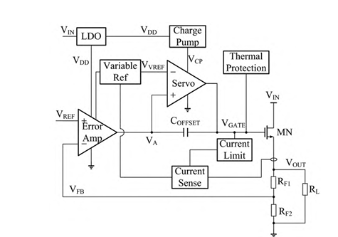
Figure 3. High PSRR Circuit[6].
3.6. Digital LDO
Digital building components are used to create the digital LDO (D-LDO). The reference voltage and output voltage are compared using a digital sensor. This sensor might be an analog-to-digital converter (ADC) or a comparator. An A-LDO often uses a digitalcontroller (integrator) in place of the EA with high VDD. This guarantees both accurate regulation and a decreased stable error. The power switch array is then turned on and off by the controller based on the necessary loading current. As a result, the all-digital D-LDO implementation benefits from process scalability and performs well in low supply voltage conditions[7][8].
Recently, the D-LDO has gained popularity because of its low power consumption and ability to work with digital circuits to scale processes. Additionally, earlier research suggested methods for reversing the standard D-LDO systems' trade-off between response time and power usage[9]. The new digital LDO strategies that strive to achieve low quiescent current and quick reaction at the same time are reviewed and discussed analytically in this study. With a reasonable sample frequency, they obtain extremely quick tracking times for the uneven transistor sizes and digital PI control approaches. The under/overshoot, however, might not be quite as optimized. Asynchronous control achieves the lowest power usage under similar circumstances. However, the quiescent current saved by the asynchronous design may not be noticeable when compared to the synchronous version when the amount of digital logic is further decreased, as in the case of the binary search. The analogue-P digital-I control method is effective for reducing undershoot as long as the analogue-assisted circuits have minimal static power consumption[10-12].
4. The Applications of LDO
There are several uses for LDOs. They are frequently seen in battery-operated gadgets where the supply voltage gradually decreases, including mp3 players and cellphones. Digital circuits, microcontrollers, and digital-to-analog converters (DACs) are a few other devices that employ LDOs when they need clean, stable power. Second, LDOs are often found in battery-operated gadgets like tablets, cellphones, portable media players, and so forth. To provide stable voltage output and extend battery life. In wireless communication systems, LDOs can be used to provide clean power to sensitive analog circuits (such as PLL, VCO, RF circuits) to reduce noise interference. In addition, LDOs are used in industrial control systems and automotive electronics for voltage regulation in high-voltage environments to ensure stable operation of devices under various power supply conditions. In audio devices, LDOs are used to provide low-noise power to ensure high-quality audio output. Among sensors, LDOs are used to power various sensors to ensure stable operation of sensors under different environmental conditions.
Circuits for LDO applications, like CAT6219. The 500mA low voltage dropout regulator CAT6219 has a quick response time to changes in line voltage and load current and has zero shutdown current and a typical ground current of 55 microamperes. It is very suitable for battery-powered devices with a power supply voltage of 2.3V to 5.5V. The specific circuit is shown in Figure 4.
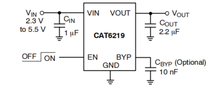
Figure 4. CAT6219.
In addition, the NCP103 was developed by Onsemi Company in figure 5. With its 150 mA LDO, the NCP103 offers engineers an extremely precise, stable, and low-noise voltage that is ideal for applications requiring a lot of space or noise. Besides, the NCP103 is very suitable for battery-powered and space-constrained applications, and it has a robust design and high reliability. Commonly used in touch screen controller power supply, wireless modules, camera power modules, MCU, and low-power FPGA power supply.
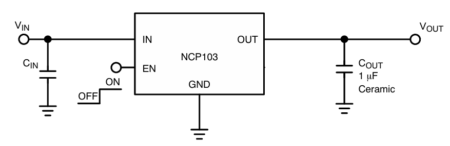
Figure 5. Typical Application Schematic of NCP103.
5. LDO development trends and challenges
5.1. LDO development trends
LDO (Low Dropout Regulator) plays an important role in modern electronic devices. Its development trends and challenges mainly include low power design, high efficiency and low dropout, high PSRR and low noise. With the popularity of portable devices and IoT devices, further reducing the power consumption of LDO has become an important trend. Low power design not only prolongs battery life, but also reduces the heat generation of the device. Improving the efficiency of LDO and reducing the dropout voltage are also current research focuses. By optimizing circuit design and adopting new materials, modern LDO can work stably at lower input voltages. Secondly, in order to meet applications that are sensitive to power supply noise (such as RF and audio circuits), the power supply rejection ratio (PSRR) and output noise performance of LDO are constantly improving. In addition, LDO design tends to support a wider input voltage range to meet the needs of different application scenarios, especially in the fields of industrial and automotive electronics. At the same time, LDO chips are also developing towards higher integration and smaller package sizes.
5.2. Challenges
In high power density and miniaturization design, thermal management of LDO becomes a major challenge. Effective heat dissipation design is essential to ensure long-term stable operation of LDO. Secondly, improving the transient response performance of LDO to cope with rapid changes in load current is a difficult point in the design. Fast transient response can ensure that the output voltage stabilizes quickly when the load changes. With the application of new materials and new processes, how to improve performance while controlling manufacturing costs is an important issue in the development of LDO. As well as for application requirements in harsh environments such as high temperature and high humidity, LDO needs to have a wider operating temperature range and better environmental adaptability.
6. Conclusion
This article classifies and introduces the basic structure of LDO, and introduces the application of LDO in different fields as well as the challenges and trends of future development. However, the article only gives a general overview of some basic LDO structures and does not propose specific structures and implementation plans. LDO is increasingly widely used in daily life, and LDO without external capacitors has become a new research hotspot. The development of LDO without external capacitors provides a new direction and foundation for subsequent research.
References
[1]. Xie H Cao W Cui K Zhao X Liu S 2024 Design of a low power and high stability LDO Electron Des Eng vol 14 pp 115-120
[2]. Sun L 2014 Principles and Applications of Linear Regulator LDO Integr Circ Appl vol 06 pp 34-37
[3]. Huang C H Liao W C 2020 A high-performance LDO regulator enabling low-power SoC with voltage scaling approaches IEEE Trans Very Large Scale Integr (VLSI) Syst vol 28 no 5 pp 1141-1149
[4]. Zhang B 2015 Design of a bandgap reference voltage source based on LDO regulator Electron Des Eng vol 24 pp 64-66
[5]. Wilson F Texas Instruments 2019 Basics of LDO August 28 2024 TI com cn
[6]. Glenn M 2014 December Understanding Low Dropout Regulators (LDOs) for System Optimization August 28 2024 Analog Devices com
[7]. Khan M Chowdhury M H 2018 May Capacitor-less low-dropout regulator (LDO) with improved PSRR and enhanced slew-rate Proc 2018 IEEE Int Symp Circuits Syst (ISCAS) pp 1-5
[8]. Morita G 2011 Noise sources in low dropout (LDO) regulators One Technol Way pp 1-12
[9]. Wu S Chen Y Huang S Xiao P Xuan Z Wu J Design of a fast transient response NMOS LDO without external capacitor Microelectron pp 1-7
[10]. Gupta H Mishra G K Rizvi N Z Patnaik S K 2016 March Design of high PSRR folded cascode operational amplifier for LDO applications Proc 2016 Int Conf Electr Electron Optim Tech (ICEEOT) pp 4617-4621
[11]. Li J 2024 A low noise high PSRR LDO design Electron Des Eng vol 08 pp 111-115 120
[12]. Huang M Lu Y 2018 October An overview of digital low drop-out regulator design Proc 2018 IEEE Asia Pac Conf Circuits Syst (APCCAS) pp 516-519
Cite this article
Yu,F. (2024). Research on the Development of LDO Chip Technology. Applied and Computational Engineering,103,24-32.
Data availability
The datasets used and/or analyzed during the current study will be available from the authors upon reasonable request.
Disclaimer/Publisher's Note
The statements, opinions and data contained in all publications are solely those of the individual author(s) and contributor(s) and not of EWA Publishing and/or the editor(s). EWA Publishing and/or the editor(s) disclaim responsibility for any injury to people or property resulting from any ideas, methods, instructions or products referred to in the content.
About volume
Volume title: Proceedings of the 2nd International Conference on Machine Learning and Automation
© 2024 by the author(s). Licensee EWA Publishing, Oxford, UK. This article is an open access article distributed under the terms and
conditions of the Creative Commons Attribution (CC BY) license. Authors who
publish this series agree to the following terms:
1. Authors retain copyright and grant the series right of first publication with the work simultaneously licensed under a Creative Commons
Attribution License that allows others to share the work with an acknowledgment of the work's authorship and initial publication in this
series.
2. Authors are able to enter into separate, additional contractual arrangements for the non-exclusive distribution of the series's published
version of the work (e.g., post it to an institutional repository or publish it in a book), with an acknowledgment of its initial
publication in this series.
3. Authors are permitted and encouraged to post their work online (e.g., in institutional repositories or on their website) prior to and
during the submission process, as it can lead to productive exchanges, as well as earlier and greater citation of published work (See
Open access policy for details).
References
[1]. Xie H Cao W Cui K Zhao X Liu S 2024 Design of a low power and high stability LDO Electron Des Eng vol 14 pp 115-120
[2]. Sun L 2014 Principles and Applications of Linear Regulator LDO Integr Circ Appl vol 06 pp 34-37
[3]. Huang C H Liao W C 2020 A high-performance LDO regulator enabling low-power SoC with voltage scaling approaches IEEE Trans Very Large Scale Integr (VLSI) Syst vol 28 no 5 pp 1141-1149
[4]. Zhang B 2015 Design of a bandgap reference voltage source based on LDO regulator Electron Des Eng vol 24 pp 64-66
[5]. Wilson F Texas Instruments 2019 Basics of LDO August 28 2024 TI com cn
[6]. Glenn M 2014 December Understanding Low Dropout Regulators (LDOs) for System Optimization August 28 2024 Analog Devices com
[7]. Khan M Chowdhury M H 2018 May Capacitor-less low-dropout regulator (LDO) with improved PSRR and enhanced slew-rate Proc 2018 IEEE Int Symp Circuits Syst (ISCAS) pp 1-5
[8]. Morita G 2011 Noise sources in low dropout (LDO) regulators One Technol Way pp 1-12
[9]. Wu S Chen Y Huang S Xiao P Xuan Z Wu J Design of a fast transient response NMOS LDO without external capacitor Microelectron pp 1-7
[10]. Gupta H Mishra G K Rizvi N Z Patnaik S K 2016 March Design of high PSRR folded cascode operational amplifier for LDO applications Proc 2016 Int Conf Electr Electron Optim Tech (ICEEOT) pp 4617-4621
[11]. Li J 2024 A low noise high PSRR LDO design Electron Des Eng vol 08 pp 111-115 120
[12]. Huang M Lu Y 2018 October An overview of digital low drop-out regulator design Proc 2018 IEEE Asia Pac Conf Circuits Syst (APCCAS) pp 516-519