


1. Introduction
We are currently in an era of information explosion, where big data and artificial intelligence are advancing rapidly. Artificial intelligence has been widely applied in various fields such as image recognition, autonomous driving, and language modeling. Behind these applications lies the continuous maturation of various neural network algorithm technologies. Neural networks comprise convolutional layers, pooling layers, and fully connected layers. Under the von Neumann architecture, the frequent movement of such massive data between storage units and computational units results in high latency and energy consumption. However, as semiconductor fabrication approaches its physical limits, Moore's Law may soon become obsolete, necessitating a method to break through the memory wall.
The emergence of memristors breaks through the von Neumann architecture by consolidating computing and storage units into a single unit, eliminating the need for frequent data movement and overcoming the bottleneck of traditional computer architectures. The computation in neural networks is analogous to synaptic connections in the human brain, possessing both network weight storage and computational capabilities. The working principle of memristors is similar to this, thus utilizing memristors to develop high-performance artificial synapses is currently an important trend in the development of high-performance AI chips and overcoming the memory wall.
2. Memristor
Chua predicted the existence of a fourth fundamental passive circuit element, the memristor, in 1971 [1], and it was manufactured by Hewlett-Packard Labs in 2008 [2]. Memristors have non-volatility, which makes them suitable for storing the weights in neural network calculations. Furthermore, the resistance of memristors can be changed by external signals, which allows the same memristor to be used for calculations at different layers of a neural network. In addition, the current calculation in memristors mainly depends on Ohm's law, which is expressed as \( I=\frac{U}{R} \) , corresponding to the weighted multiplication operations in neural networks. Based on the above three characteristics, memristors have been widely studied and applied in the development of neural network computing chips.
2.1. Memory Technology Utilizing Memristive Effect
RRAM is a memory technology that utilizes the memristive effect. The basic structure of an RRAM cell consists of a layer of semiconductor thin film between two electrodes. When a voltage is applied across the two terminals of the RRAM cell, one or more conductive filaments composed of holes will form, which varies depending on the polarity of the voltage. The thicker and more conductive the filaments, the lower the resistance. As shown in Figure 1, the current is directly proportional to the size of the conductive filament. When the device is in a forward-biased state, oxygen atoms are knocked out of the lattice to become negatively charged oxygen ions. Under the influence of the forward electric field, these oxygen ions drift towards the anode, leaving behind corresponding oxygen vacancies in the metal oxide layer [3].
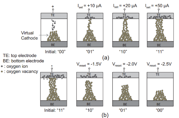
Figure 1: (a) the formation process of conductive filaments in bipolar RRAM cells; (b) the relationship between the conductive filaments and the applied voltage [3]
By designing a crossbar array, weight storage in neural network computations can be achieved. The resistance values can be refreshed by inputting different currents or voltages, similar to setting the weights for each layer of a neural network. As shown in Figure 2, this array design converts analog signals through DAC for computation, then converts them back to digital signals through ADC for output. Additionally, voltage is applied at both ends to refresh the resistance values (weights). This represents the simplest design of a memristor crossbar array, where each cell corresponds to the RRAM cell mentioned earlier.
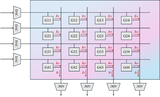
Figure 2: Memristor cross-array design
2.2. Architecture
Research on the architecture of memristor chips has gradually matured, and all of them improve computing efficiency by reducing data transmission. However, each architecture has its own advantages and disadvantages. For example, PRIME has higher programmability, but also higher design complexity, which leads to challenges in tight hardware integration. The ISACC architecture is more energy efficient in large-scale parallel processing tasks, but lacks programmability. The choice of architecture needs to be determined based on the specific functions that the chip needs to achieve.
2.2.1. RENO
In 2015, a research team from the University of Pittsburgh in the United States proposed the RENO architecture. This was the first architecture to study the connection relationship of memristor arrays on chips and discuss the communication methods between AI acceleration units and controllers [4]. As depicted in Figure 4(a), the intersections of horizontal and vertical lines represent memristor arrays, while circles denote different routers. The architecture adopts a star-shaped topology for interconnection. Figure 4(b) illustrates that the architecture employs mixed signals (digital and analog signals) for transmission, with digital signals used for selecting routing paths and analog signals utilized for transmitting the computation results of the array. However, this architecture still has some issues; for instance, computation results cannot be cached, and hardware implementation costs cannot be reduced through methods such as weight and intermediate result reuse [5].
(a) |
(b) |
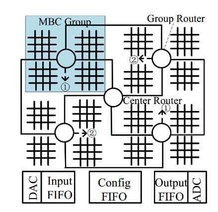
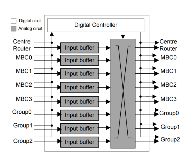
Figure 3: The RENO architecture; (a) Architecture using a star topology; (b) architecture using mixed signals (digital and analog) for transmission [5]
2.2.2. PRIME
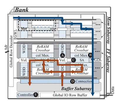
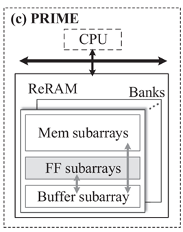
The PRIME architecture introduces a novel caching strategy, as shown in Figure 4(a). The architecture divides the ReRAM memory into three regions: the storage sub-array, the full-function sub-array, and the buffer sub-array. The full-function sub-array has both computing and data storage capabilities [6]. In addition, the calculation results of each module are converted to digital form before being output to the cache in the register. However, there is still room for improvement in this structure. As shown in Figure 4(b), the orange lines represent computational data flow, while the blue lines represent storage of computational flow. The star-shaped topology of the interconnection structure in this architecture leads to increased data transmission pressure on the top-level routes. Additionally, its interconnection via buses may cause a decrease in transmission efficiency due to the arbitration cost of buses [5].
(a) (b)
Figure 4: PRIME; (a) The ReRAM memory is divided into three areas; (b)The star-shaped topology interconnection structure [6]
2.2.3. ISAAC
ISAAC architecture has similarities with the DaDianNao architecture. It employs numerous interconnected nodes, with each node structured by a set of tiles. However, the internal structure of each tile and IMA differs [7]. The specific architecture is illustrated in Figure 5. The ISAAC architecture adopts a hierarchical hybrid topology for better scalability and flexibility, and uses a centralized grid interconnection for all units. Internally, each unit uses a bus interconnection structure to facilitate efficient transmission between adjacent arrays. Furthermore, using a multi-core architecture, the ISAAC architecture assigns the convolutional layer to different memristor arrays, which operate in parallel pipelines [7]. However, this architecture does not fully consider the data and weight reuse strategy in neural networks, and its programmability is slightly inferior to PRIME.
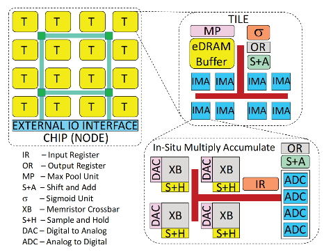
Figure 5: ISAAC architecture [7]
2.2.4. MAX2
Since the ISACC structure does not consider the weight reuse strategy in neural networks, Mao et al. proposed the MAX2 architecture, which discusses data reuse and area utilization [8-9]. MAX2 is based on a multi-level multi-array architecture similar to ISACC, and uses a pulse array architecture and a strategy of network weight replication and input feature map reuse. This improves the data reuse rate, greatly reduces the need for data movement between processing units, and improves time, energy, and area utilization.
3. Neuromorphic chip
At the same or even lower manufacturing process nodes, due to the characteristics of memristors, the performance achievable by integrated chips may far exceed that of chips based on conventional CMOS technology. As research on memristor-based architectures gradually matures, many teams have begun to utilize CMOS to build peripheral circuits integrated on chips to achieve complete computational functions. Moreover, they continuously increase the number of arrays to enhance computational power. Presently, memristor-based brain-like computing units typically include control circuits, pre-neurons, memristor crossbar arrays, post-neurons, and cache areas as the main components. These units then interact with the main processor for input and output operations.
3.1. Memristive crossbar
Currently, the most basic memristor array structures include 1R, 1T1R, 1D1R and 1S1R structures, with the most commonly used being the 1R and 1T1R structures. The advantage of the 1R structure lies in its simple array structure. However, during computation, the influence of leakage current is significant, making the design of peripheral CMOS circuits more challenging. The 1T1R structure connects the drain of a transistor to the memristor, allowing precise control of the current passing through the memristor in series, thereby achieving multi-level conductance programming. The transistor also alleviates sneak path current and half-select issues during array programming and reading. [10] At the same time, there are also other design strategies, such as the design of multi-layered cakes and the use of positive and negative weights, to improve stability.
3.2. Research status
Wu et al. designed the world's first fully functional memristor-based brain-inspired chip, which integrates two 784 × 100-scale and two 100 × 10-scale 1T1R memristor arrays as synapses between input neurons and hidden neurons, and between hidden neurons and output neurons [11]. A handwriting recognition network is run on this chip, with an accuracy loss of less than 5% compared to a full-precision network.
In addition, the chip designed with the 1R memristor array integrates a 54×108-scale 1R memristor array, in which the passivation layer isolates the CMOS circuit from the memristor, similar to the multi-layer cake design mentioned earlier. However, this design clearly shows the shortcomings of the 1R memristor array, which may pose significant challenges for the design of peripheral circuits. In this design, the area of the memristor array is only 0.14 mm2, but the total chip area is 61.64 mm2 [12]. On this basis, the chip has been upgraded, the original configuration of two 1T1R arrays has been optimized to one 2T2R array, and the external circuit for readout operation has been simplified. As a result, the accuracy loss in the handwriting recognition network has been reduced to 2% [13].
4. Conclusion
Research on neuromorphic chips based on memristors has gradually matured, and it has been confirmed that memristors do provide practical assistance for the design of artificial intelligence accelerators and neuromorphic chips. However, there are still many challenges in improving the design of memristors. First, the nonlinearity of the resistance change of memristors affects the design. In fact, the resistance change of most memristors is nonlinear, resulting in fewer available resistance states in mass-produced arrays. Therefore, the manufacturing process of memristors still needs to be strengthened. Furthermore, there is a certain degree of complexity in the peripheral circuitry of memristors. Although the use of arrays such as 1T1R or 2T2R has greatly improved the design of peripheral circuits compared to chips based on 1R structures, they are still too complex. The presence of a large number of ADC and DAC modules may even negate the advantages of high integration and low power consumption of the memristor itself [14]. In addition, multi-array neuromorphic computing architectures currently have their own advantages and disadvantages, and it is hoped that better architectures will emerge. At the same time, research on related programming and datasets is still relatively lacking. Current research mainly focuses on sparse coding [15-16].
References
[1]. Chua, L.O. (1971). Memristor-The missing circuit element. IEEE Transactions on Circuit Theory, 18, 507-519.
[2]. Strukov, D.B., Snider, G., Stewart, D.R., & Williams, R.S. (2008). The missing memristor found. Nature, 453, 80-83.
[3]. Xu, C., Niu, D., Muralimanohar, N., Jouppi, N.P., & Xie, Y. (2013). Understanding the trade-offs in multi-level cell ReRAM memory design. 2013 50th ACM/EDAC/IEEE Design Automation Conference (DAC), 1-6.
[4]. Liu, X., Mao, M., Liu, B., Li, H., Chen, Y., Li, B., Wang, Y., Jiang, H., Barnell, M., Wu, Q., & Yang, J. (2015). RENO: A high-efficient reconfigurable neuromorphic computing accelerator design. In Proceedings of the 52nd Annual Design Automation Conference (DAC '15) (pp. 1-6). Association for Computing Machinery, New York, NY, USA. Article 66.
[5]. Chen C, Luo, C, Liu, S & Liu, H.(2023). Review of the current research status of memristor-based brain computing chips. Journal of National University of Defense Technology, (01), 1-14.
[6]. Chi, P., Li, S., Xu, C., Tao, Z., Zhao, J., Liu, Y., Wang, Y., & Xie, Y. (2023). PRIME: A Novel Processing-in-memory Architecture for Neural Network Computation in ReRAM-based Main Memory.
[7]. Shafiee, A., Nag, A., Muralimanohar, N., Balasubramonian, R., Strachan, J.P., Hu, M., Williams, R.S., & Srikumar, V. (2016). ISAAC: A Convolutional Neural Network Accelerator with In-Situ Analog Arithmetic in Crossbars. 2016 ACM/IEEE 43rd Annual International Symposium on Computer Architecture (ISCA), 14-26.
[8]. Mao, M., Peng, X., Liu, R., Li, J., Yu, S., & Chakrabarti, C. (2019). MAX2: An ReRAM-Based Neural Network Accelerator That Maximizes Data Reuse and Area Utilization. IEEE Journal on Emerging and Selected Topics in Circuits and Systems, 9, 398-410.
[9]. Song, L., Qian, X., Li, H.H., & Chen, Y. (2017). PipeLayer: A Pipelined ReRAM-Based Accelerator for Deep Learning. 2017 IEEE International Symposium on High Performance Computer Architecture (HPCA), 541-552.
[10]. Xia, Q., & Yang, J.J. (2019). Memristive crossbar arrays for brain-inspired computing. Nature Materials, 18, 309-323.
[11]. Wu, H., Yao, P., Gao, B., Wu, W., Zhang, Q., Zhang, W., Deng, N., Wu, D., Wong, H.-., Yu, S., & Qian, H. (2017). Device and circuit optimization of RRAM for neuromorphic computing. 2017 IEEE International Electron Devices Meeting (IEDM), 11.5.1-11.5.4.
[12]. Cai, F., Correll, J.M., Lee, S.H., Lim, Y., Bothra, V., Zhang, Z., Flynn, M.P., & Lu, W. (2019). A fully integrated reprogrammable memristor–CMOS system for efficient multiply–accumulate operations. Nature Electronics, 2, 290 - 299.
[13]. Liu, Q., Gao, B., Yao, P., Wu, D., Chen, J., Pang, Y., Zhang, W., Liao, Y., Xue, C., Chen, W., Tang, J., Wang, Y., Chang, M., Qian, H., & Wu, H. (2020). 33.2 A Fully Integrated Analog ReRAM Based 78.4TOPS/W Compute-In-Memory Chip with Fully Parallel MAC Computing. 2020 IEEE International Solid- State Circuits Conference - (ISSCC), 500-502.
[14]. Ambrogio, S., Narayanan, P., Okazaki, A., Fasoli, A., Mackin, C., Hosokawa, K., Nomura, A., Yasuda, T., Chen, A., Friz, A.M., Ishii, M., Luquin, J., Kohda, Y., Saulnier, N., Brew, K., Choi, S., Ok, I., Philip, T., Chan, V., Silvestre, M.C., Ahsan, I., Narayanan, V., Tsai, H., & Burr, G.W. (2023). An analog-AI chip for energy-efficient speech recognition and transcription. Nature, 620, 768 - 775.
[15]. Li, J., Ren, S., Li, Y., Yang, L., Yu, Y., Ni, R., Zhou, H., Bao, H., He, Y., Chen, J., Jia, H., & Miao, X. (2023). Sparse matrix multiplication in a record-low power self-rectifying memristor array for scientific computing. Science Advances, 9.
[16]. Yao, P., Gao, B., & Wu, H. (2024). Transforming edge hardware with in situ learning features. Nature Reviews Electrical Engineering.
Cite this article
Fan,L. (2025). Research Progress of Neuromorphic Chips. Applied and Computational Engineering,125,1-7.
Data availability
The datasets used and/or analyzed during the current study will be available from the authors upon reasonable request.
Disclaimer/Publisher's Note
The statements, opinions and data contained in all publications are solely those of the individual author(s) and contributor(s) and not of EWA Publishing and/or the editor(s). EWA Publishing and/or the editor(s) disclaim responsibility for any injury to people or property resulting from any ideas, methods, instructions or products referred to in the content.
About volume
Volume title: Proceedings of the 3rd International Conference on Mechatronics and Smart Systems
© 2024 by the author(s). Licensee EWA Publishing, Oxford, UK. This article is an open access article distributed under the terms and
conditions of the Creative Commons Attribution (CC BY) license. Authors who
publish this series agree to the following terms:
1. Authors retain copyright and grant the series right of first publication with the work simultaneously licensed under a Creative Commons
Attribution License that allows others to share the work with an acknowledgment of the work's authorship and initial publication in this
series.
2. Authors are able to enter into separate, additional contractual arrangements for the non-exclusive distribution of the series's published
version of the work (e.g., post it to an institutional repository or publish it in a book), with an acknowledgment of its initial
publication in this series.
3. Authors are permitted and encouraged to post their work online (e.g., in institutional repositories or on their website) prior to and
during the submission process, as it can lead to productive exchanges, as well as earlier and greater citation of published work (See
Open access policy for details).
References
[1]. Chua, L.O. (1971). Memristor-The missing circuit element. IEEE Transactions on Circuit Theory, 18, 507-519.
[2]. Strukov, D.B., Snider, G., Stewart, D.R., & Williams, R.S. (2008). The missing memristor found. Nature, 453, 80-83.
[3]. Xu, C., Niu, D., Muralimanohar, N., Jouppi, N.P., & Xie, Y. (2013). Understanding the trade-offs in multi-level cell ReRAM memory design. 2013 50th ACM/EDAC/IEEE Design Automation Conference (DAC), 1-6.
[4]. Liu, X., Mao, M., Liu, B., Li, H., Chen, Y., Li, B., Wang, Y., Jiang, H., Barnell, M., Wu, Q., & Yang, J. (2015). RENO: A high-efficient reconfigurable neuromorphic computing accelerator design. In Proceedings of the 52nd Annual Design Automation Conference (DAC '15) (pp. 1-6). Association for Computing Machinery, New York, NY, USA. Article 66.
[5]. Chen C, Luo, C, Liu, S & Liu, H.(2023). Review of the current research status of memristor-based brain computing chips. Journal of National University of Defense Technology, (01), 1-14.
[6]. Chi, P., Li, S., Xu, C., Tao, Z., Zhao, J., Liu, Y., Wang, Y., & Xie, Y. (2023). PRIME: A Novel Processing-in-memory Architecture for Neural Network Computation in ReRAM-based Main Memory.
[7]. Shafiee, A., Nag, A., Muralimanohar, N., Balasubramonian, R., Strachan, J.P., Hu, M., Williams, R.S., & Srikumar, V. (2016). ISAAC: A Convolutional Neural Network Accelerator with In-Situ Analog Arithmetic in Crossbars. 2016 ACM/IEEE 43rd Annual International Symposium on Computer Architecture (ISCA), 14-26.
[8]. Mao, M., Peng, X., Liu, R., Li, J., Yu, S., & Chakrabarti, C. (2019). MAX2: An ReRAM-Based Neural Network Accelerator That Maximizes Data Reuse and Area Utilization. IEEE Journal on Emerging and Selected Topics in Circuits and Systems, 9, 398-410.
[9]. Song, L., Qian, X., Li, H.H., & Chen, Y. (2017). PipeLayer: A Pipelined ReRAM-Based Accelerator for Deep Learning. 2017 IEEE International Symposium on High Performance Computer Architecture (HPCA), 541-552.
[10]. Xia, Q., & Yang, J.J. (2019). Memristive crossbar arrays for brain-inspired computing. Nature Materials, 18, 309-323.
[11]. Wu, H., Yao, P., Gao, B., Wu, W., Zhang, Q., Zhang, W., Deng, N., Wu, D., Wong, H.-., Yu, S., & Qian, H. (2017). Device and circuit optimization of RRAM for neuromorphic computing. 2017 IEEE International Electron Devices Meeting (IEDM), 11.5.1-11.5.4.
[12]. Cai, F., Correll, J.M., Lee, S.H., Lim, Y., Bothra, V., Zhang, Z., Flynn, M.P., & Lu, W. (2019). A fully integrated reprogrammable memristor–CMOS system for efficient multiply–accumulate operations. Nature Electronics, 2, 290 - 299.
[13]. Liu, Q., Gao, B., Yao, P., Wu, D., Chen, J., Pang, Y., Zhang, W., Liao, Y., Xue, C., Chen, W., Tang, J., Wang, Y., Chang, M., Qian, H., & Wu, H. (2020). 33.2 A Fully Integrated Analog ReRAM Based 78.4TOPS/W Compute-In-Memory Chip with Fully Parallel MAC Computing. 2020 IEEE International Solid- State Circuits Conference - (ISSCC), 500-502.
[14]. Ambrogio, S., Narayanan, P., Okazaki, A., Fasoli, A., Mackin, C., Hosokawa, K., Nomura, A., Yasuda, T., Chen, A., Friz, A.M., Ishii, M., Luquin, J., Kohda, Y., Saulnier, N., Brew, K., Choi, S., Ok, I., Philip, T., Chan, V., Silvestre, M.C., Ahsan, I., Narayanan, V., Tsai, H., & Burr, G.W. (2023). An analog-AI chip for energy-efficient speech recognition and transcription. Nature, 620, 768 - 775.
[15]. Li, J., Ren, S., Li, Y., Yang, L., Yu, Y., Ni, R., Zhou, H., Bao, H., He, Y., Chen, J., Jia, H., & Miao, X. (2023). Sparse matrix multiplication in a record-low power self-rectifying memristor array for scientific computing. Science Advances, 9.
[16]. Yao, P., Gao, B., & Wu, H. (2024). Transforming edge hardware with in situ learning features. Nature Reviews Electrical Engineering.