


1. Introduction
In the health monitoring of wearable devices, the system consists of analog front-end and digital back-end circuits, and the analog-to-digital converter (ADC) plays an important role as a key bridge. The analog front-end includes an instrumentation amplifier and a programmable gain amplifier, while the digital back-end consists of a central processing unit (CPU) and a wireless transceiver module. The CPU analyzes the digital signal converted by the ADC and feeds back the results to the user in real time, highlighting the core position of the ADC [1]. Typical ADC architectures include successive approximation ADC (SAR ADC), flash ADC, pipeline ADC, and Sigma Delta ADC, and a variety of single architectures and emerging hybrid architectures. Among these types, SAR ADC stands out for its relatively simple structure. The main circuit modules include sampling circuit, DAC, comparator, and SAR logic circuit. Most components are digital structures or switched capacitor structures, and the main analog unit is the comparator. Compared with other ADC types, SAR ADC can benefit more from the reduction of CMOS process feature size. Process advances have also made it possible to reduce the power supply voltage, which helps to further reduce the power consumption of the digital part [2-6]. This paper employs a literature review to explore the application of low-power SAR ADCs in bioelectric signal acquisition, thus addressing the challenge of limited battery life in wearable devices. Through the analysis of related studies, the design advantages and energy efficiency of SAR ADCs are discussed, providing insights for future technology optimization.
2. Overview of Low-Power SAR ADC Design
2.1. Key Technologies of SAR ADC
2.1.1. Sampling and Holding Circuit
The complementary sampling and holding circuit effectively reduces the impact of on-resistance and body effect on the output by interconnecting the source and drain of NMOS and PMOS. Optimally, regardless of the CLK signal's state, one tube should always be in the on state while the other remains off to achieve a complementary effect [7]. Figure 1 shows a simple complementary sampling switch, which uses the opposite charge polarity of NMOS and PMOS. When the charges of the two are equal, the channel charge injection effect can be offset, thus reducing the input offset error. However, in order to achieve a low-power ADC, the power supply voltage is usually limited to less than 1V, which may cause the threshold voltage to be higher than the power supply voltage, thereby affecting the on state of the MOS switch.
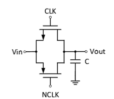
Figure 1: Complementary Sampling Switch
2.1.2. Comparator
The Strong-Arm dynamic comparator operates in four stages, with its typical circuit diagram illustrated in Figure 2 [8]. First, in the reset stage, when the clock signal clkc is low, M7 and M10 are turned on, and VOUTP, VOUTN, VX+ and VX- are pulled up to VDD to complete the reset operation. Then it enters the preamplification stage, at which time clkc is high, the tail current tube Mb is turned on, and M1 and M2 discharge the VX+ and VX- nodes at different speeds according to the size of the input signal. When VX+ or VX- drops to VDD - |Vthp|, the comparator enters the weak positive feedback stage, at which time M3 and M4 discharge the VOUTP and VOUTN nodes in turn to enhance the stability of the output. In the final strong positive feedback stage, when VOUTP or VOUTN falls to VDD - |Vthp|, M6 or M5 turns on, fully activating the positive feedback loop. This enables the comparator to quickly latch and output the comparison result. These four stages enable the Strong-Arm dynamic comparator to perform signal comparisons efficiently.
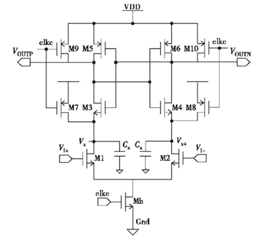
Figure 2: Strong-Arm Dynamic Comparator
2.1.3. DAC Capacitor Array
The traditional switching strategy employs the lower plate sampling method. During the sampling stage, the upper plate switch of the capacitor is closed, connecting the reference voltage Vcm to the capacitor array at both the in-phase and inverting ends, while the differential input signals Vin and Vip are linked to the lower plate of the capacitor. After the sampling is completed, the upper plate switch of the capacitor is disconnected, the capacitor is charged, and Vin and Vip of the lower plate are also disconnected. At this time, the highest bit reference voltage of the in-phase end capacitor array is set to Vref, and the rest are connected to GND, resulting in the output of the in-phase end being Vref - Vip; the inverting end capacitor array is the opposite, the highest bit is connected to GND, the rest are connected to Vref, and the inverting end output becomes Vref - Vin. Next, the comparator performs the first comparison and outputs the highest bit digital code. Figure 3 shows the switching process of the 3-bit traditional switching strategy DAC capacitor array [9].
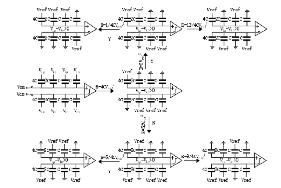
Figure 3: DAC Capacitor Array of 3-bit Traditional Switching Strategy
According to the change of the digital code output by the highest bit, the reference voltage on the lower plate of the capacitor will jump. Taking the capacitor array at the same phase end as an example, when the digital code output by the highest bit is 1, the reference voltage connected to the highest capacitor remains unchanged; when the digital code is 0, the reference voltage of the highest capacitor changes from Vref to GND. The principle of the inverting end is the same, but the direction of change is opposite. The changes of each subsequent bit follow the same rule until the complete digital code is output. This switching strategy is to preset the comparison result to 1 before each comparison. If the actual comparison result is consistent with the preset, the output remains unchanged; if not, a jump switch is required. Since the lower plate of the capacitor jumps between three states, the design is relatively complex and the power consumption is high.
2.1.4. SAR Logic
SAR logic is an important part of SAR ADC, which is responsible for storing the comparison results of the comparator and controlling the flipping of the capacitor array. Traditional SAR logic is implemented using synchronous logic composed of D flip-flops, requiring synchronous clock drive, and the synchronous clock frequency is usually much higher than the sampling frequency \( {f_{s}} \) . For N-bit SAR ADC, the required synchronous clock frequency is at least (N+1) \( {f_{s}} \) [10]. As shown in Figure 4, CLKS is the sampling clock, CLK is the synchronous clock signal, and COMP is the comparison result of the comparator. CLKC is generated by the OR operation of CLKS, CLK0 and CLK as the control clock of the comparator. When CLKS is high (i.e., the sampling stage), CLK12 to CLK0 are set to 0, D12 and D6 are set to 1, and D7 to D11 and D0 to D5 are set to 0. After sampling is completed, with the rising edge of the CLK clock, CLK12 to CLK0 change from low to high in turn, forming a storage timing, as shown in Figure 4. The storage timing is used to control the output result of the comparator, so that D12 becomes D0, and is fed back to the capacitor array, thereby adjusting the upper plate voltage of the capacitor array, gradually approaching the input signal, and completing the A/D conversion process.
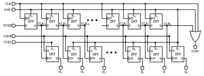
Figure 4: Synchronous SAR Logic
2.2. Low-Power Design Requirements and Strategies
2.2.1. Overall Design Architecture of Low-Power SAR ADC
The overall circuit structure is shown in Figure 5. First, the improved gate bootstrap sample-and-hold circuit samples the analog input signal and adopts a differential input method to suppress common-mode noise. Next, after comparison by two-stage pre-dynamic comparators, the comparison results are stored by the dynamic SAR control logic circuit, and the processed signal is sent to the DAC capacitor array. The DAC capacitor array adopts a monotonic switching strategy based on the common-mode voltage to change the input signal at both ends of the comparator before the next comparison. By repeating this operation n times, an n-bit digital code can be obtained. Compared with the traditional SAR ADC, the focus is on improving and optimizing the switching strategy of the sample-and-hold circuit, comparator, and DAC capacitor array, thereby effectively reducing the power consumption and chip area of the ADC circuit.
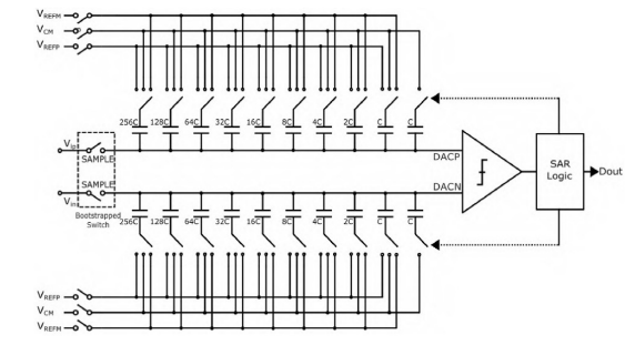
Figure 5: Overall Design Architecture of Low-Power SAR ADC
2.2.2. Bootstrapped Switch Circuit
Figure 6 shows the circuit diagram of the Bootstrapped Switch circuit. CLKS and CLKSB are a pair of anti-phase clocks, and only one side is simplified for analysis below. When CLKS is “0” and CLKSB is “1”, since M12 is turned on, the gate voltages of M4, M6 and M9 are discharged to the “0” potential. At this time, M3 and M4 are turned on, the top plate node potential of capacitor C1 is “1”, and the bottom plate node potential is “0”, and a potential difference VDD is formed on the capacitor. At this time, M7, M8 and sampling switch M9 are all turned off. When CLKS becomes “1” and CLKSB becomes “0”, M3 and M1 are turned off, while M2, M7 and M8 are turned on. At this time, the bottom plate node voltage of capacitor C1 is VIP, and the top plate node voltage is VDD + VIP. The drain potential of M2 and M6 is VIP, and M5 is turned on. Since M12 is turned off, the gate potentials of M4, M6 and M9 are VDD + VIP, and the sampling switch M9 is turned on. The switching speed of the switch tube is independent of the charging speed of capacitor C1 and is solely determined by the clock signal. With M4 cut off, the gate voltage of M9 remains at VDD + VIP throughout the entire on-time, ensuring that the gate-source voltage VGS of M9 is VDD. This ensures stable on-resistance and good linearity in the sampling circuit.
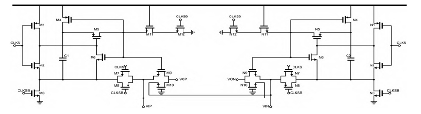
Figure 6: Bootstrapped Switch Circuit
2.2.3. DAC Capacitor Array
The switching scheme of the DAC capacitor array adopts the MCS method, as shown in Figure 7. During the sampling phase, the top plate of the capacitor is charged to Vin/Vip, and the bottom plate potential is reset to the common mode voltage VCM. After the sampling is completed, the top plate of the capacitor is disconnected from Vin/Vip, and the comparator starts the first comparison. If Vip > Vin, the most significant bit (MSB) is “1”, at which time the maximum capacitor bottom plate at the DACP end is switched to the negative reference voltage VREFM, and the maximum capacitor bottom plate at the DACN end is switched to the positive reference voltage VREFP; conversely, if Vip < Vin, the MSB is “0”, the maximum capacitor bottom plate at the DACN end is switched to the negative reference voltage VREFM, and the maximum capacitor bottom plate at the DACP end is switched to the positive reference voltage VREFP. Subsequently, the DAC array redistributes the charge. This process is repeated until the least significant bit (LSB) is determined.
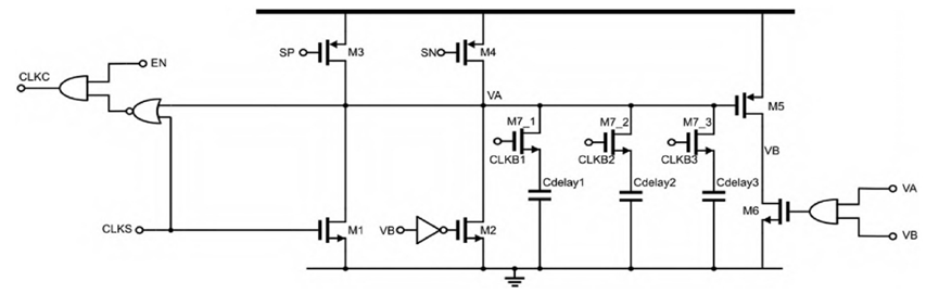
Figure 7: MCS DAC Capacitor Array
Compared with the traditional switching method, MCS can save more power in the DAC [11]. An n-bit MCS SAR ADC requires 2(n-1) unit capacitors. The switching energy in MCS is dependent on the output code, and the expression for its average switching energy consumption can be expressed as:
\( {E_{avg}}=\sum _{i=1}^{n-1}{2^{n-i-2}}·({2^{-i}})·C·V_{ref}^{2} \) (1)
For a 10-bit SAR ADC, its average switching power consumption is 170.167 times C times V_ref squared, and the required switching energy is 87.6% less than that of the traditional scheme [12].
2.2.4. Comparator
The performance of the comparator is crucial to the accuracy of the SAR ADC because it directly affects the accuracy of the output results. Despite its low power consumption, the dynamic comparator often has significant offset error that typically requires calibration, complicating the design process. Related research proposed a Sat-level preamplifier dynamic comparator structure, which consists of a preamplifier and a post-stage dynamic latch comparator circuit. The input signal is first amplified by the preamplifier and then enters the latch comparator circuit. Before the signal enters the latch comparator circuit, the preamplifier amplifies it, and there is a positive feedback relationship between the two. The two differential voltages output by the latch comparator circuit become the final output of the comparator after passing through the SR latch [13]. This design effectively minimizes noise and input offset voltage in the comparator. And the two-stage structure integrates the amplifier and dynamic latch comparator, achieving low power consumption and minimizing input offset voltage.
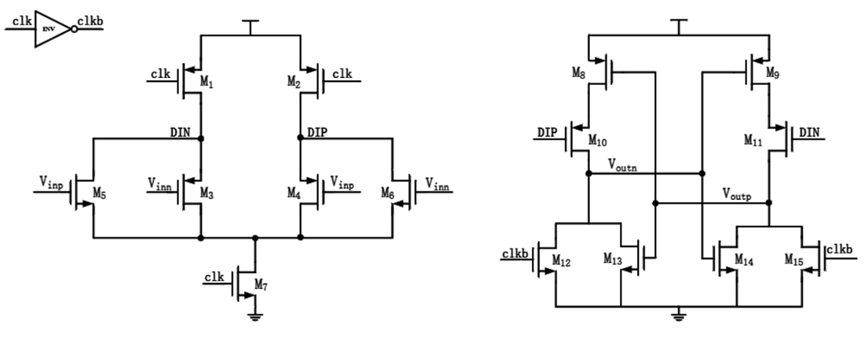
Figure 8: (a) Preamplifier Structure, (b) Latch Structure
The dynamic latch comparator consists of a preamplifier and a latch, wherein the structure of the preamplifier is shown in Figure 8(a), and the structure of the latch is shown in Figure 8(b). When clk=0 and clkb=1, the comparator is in a reset state, M1 and M2 are turned on, and the output terminals DIP and DIN are pulled up to VDD, M10 and M11 are turned off, M12 and M15 are turned on, and the output terminals Voutp and Voutn are pulled down to zero. When clk=1 and clkb=0, the comparator enters a regeneration state, M1 and M2 are turned off, M7 is turned on, and the voltages of DIP and DIN drop from VDD. The drop speed is determined by the input voltages Vinn and Vinp, resulting in different voltages of Voutp and Voutn. M12 and M15 are turned off, and the latch pulls the lower voltage to zero and the higher voltage to VDD through positive feedback to achieve signal comparison, and the voltage is reset at the next reset. M8, M9, M13, and M14 are the core components of the latch, while M10 and M11 enhance the common mode rejection ratio (CMRR), and M12 and M15 function as voltage reset switches.
3. Application of SAR ADC in Heart Rate and Blood Oxygen Monitoring
Photoplethysmographic volumetric tracing (PPG) is a non-invasive optical method that leverages light absorption principles to detect volume changes in peripheral blood circulation throughout the cardiac cycle. It differentiates arterial pulses and offers insights into cardiovascular dynamics, blood oxygen saturation (SpO2), and even emotional states. The PPG sensor system includes a light-emitting diode (LED) driver block, LEDs, photodetectors (PDs), and a data acquisition block [14]. The driver block controls the LEDs to emit specific wavelengths of light that penetrate the skin and tissues; the corresponding photons are absorbed, scattered, or reflected by the blood vessels underneath, and the intensity of the reflected light changes due to the change in blood volume with each heartbeat. The reflected light is converted into photocurrent by the PD. Finally, the data acquisition module is used for analog signal processing to convert the photocurrent into digital codes. These digital codes are further processed to obtain the raw PPG signal. The light-to-digital converter (LDC) is an important part of the photoelectric volumetric tracing (PPG) readout chain. Optical digitizers can be simply categorized into transimpedance amplifier (TIA)-based optical digitizers (shown in Figure 9(a)) and optical digitizers without TIA (shown in Figure 9(b)) [15].
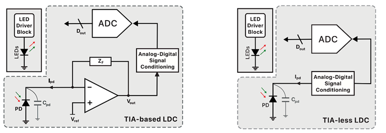
Figure 9: (a) Optical Digital Conversion with Transimpedance Amplifier (TIA), (b). Optical Digital Converter without TIA
In the PPG sensor system, the ADC is crucial for converting the weak analog PPG signal detected by the PD into a digital signal for further processing and analysis. The performance of the ADC, including resolution, dynamic range, power consumption, and conversion rate, directly affects the quality of the PPG signal and the overall performance of the sensor system [16]. To minimize system power consumption, particularly that of the LED, a low-power SAR ADC system can be employed, facilitating the advancement of PPG sensor technology in wearable health monitoring devices.
4. Technical Challenges and Future Development
In wearable devices, SAR ADC design faces numerous technical challenges, particularly in balancing power consumption and performance. As wearable devices demand longer battery life, minimizing power consumption without sacrificing conversion speed and resolution is crucial, requiring advanced circuit design and innovative algorithms. Meanwhile, enhancing integration presents a significant challenge. As devices trend toward miniaturization and portability, integrating high-performance SAR ADCs in confined spaces requires advanced manufacturing processes and compact circuit design. In addition, the suppression of environmental interference cannot be ignored, because wearable devices will be affected by various environmental factors in actual use. Improving the anti-interference ability of ADC is crucial to its reliability, which may require the use of more complex signal processing techniques and improved shielding designs. In the future, with the development of more advanced CMOS processes, SAR ADCs may achieve lower power consumption and higher integration, which will help to manufacture smaller and more efficient wearable devices.
5. Conclusion
This study investigates the design of low-power SAR ADCs for wearable health monitoring devices, emphasizing design principles, key technologies, and performance metrics, and achieving several important results. Through the optimized design of the sample-and-hold circuit, comparator, DAC capacitor array and SAR logic, the power consumption was significantly reduced on the basis of high precision and high resolution. For example, the enhanced gate bootstrap sample-and-hold circuit effectively suppressed common-mode noise and ensured linearity; the DAC capacitor array employed a monotonic switching strategy based on common-mode voltage (MCS); and the comparator design featured a two-stage preamplifier dynamic comparator structure. These innovations have positioned SAR ADCs for significant application potential in health monitoring, including heart rate and blood oxygen monitoring. However, in practical applications, circuit design may require further optimization to accommodate complex environments and higher performance demands. Despite significant progress in reducing power consumption, SAR ADC performance can still be impacted by extreme conditions, such as strong electromagnetic interference, highlighting the need for more effective anti-interference measures in future research.
References
[1]. Zhang, J.C. (2024) Design of Low Power SAR ADC for Wearable Medical Devices. Qingdao University of Technology.
[2]. Mekkattillam, Y., Mohapatra, S. and Mohapatra, N.R. (2019) Design and Calibration of 14-bit 10 KS/s Low Power SAR ADC for Bio-medical Applications. VLSI Design and Test: 23rd International Symposium, 590-604.
[3]. Tong, X. and Ghovanloo, M. (2015) Energy-efficient switching scheme in SAR ADC for biomedical electronics[J]. Electronics Letters, 51(9): 676-678.
[4]. Hesener, M., et al. A 14b 40MS/s redundant SAR ADC with 480MHz Clock in 0.13 μm CMOS. IEEE International Solid-State Circuits Conference, Digest of Technical Papers. 248-600.
[5]. Li, S., et al. A 13-ENOB second-order noise-shaping SAR ADC realizing optimized NTF zeros using the error-feedback structure. IEEE Journal of Solid-State Circuits, 53(12): 3484-3496.
[6]. Tai, H.Y., et al. (2014) 11.2 A 0.85 fJ/conversion-step 10b 200kS/s subranging SAR ADC in 40nm CMOS. ISSCC, 196-197.
[7]. Shi, L.T. (2024) Research and Design of High-Precision SAR ADC. University of Electronic Science and Technology of China.
[8]. van Elzakker, M., et al. (2010) A 10-bit charge-redistribution ADC consuming 1.9 μW at 1 MS/s. IEEE Journal of Solid-State Circuits, 45(5): 1007-1015.
[9]. Shi, L., et al. (2018) A 13b-ENOB noise shaping SAR ADC with a two-capacitor DAC. 61st International Midwest Symposium on Circuits and Systems (MWSCAS). 153-156.
[10]. Liu, C.C., et al. (2010) A 10-bit 50-MS/s SAR ADC with a monotonic capacitor switching procedure. IEEE Journal of Solid-State Circuits, 45(4): 731-740.
[11]. Ginsburg, B.P. and Chandrakasan, A.P. (2005) An energy-efficient charge recycling approach for a SAR converter with capacitive DAC. IEEE Int. Symp. on Circuits and Systems.
[12]. Hariprasath, V., Guerber, J., et al. (2010) Merged capacitor switching based SAR ADC with highest switching energy-efficiency. ELECTRONICS LETTERS, 46(9).
[13]. Li, Y., Zhou, Y. and Chiu, Y. (2020) A compact calibration model for linearizing CMOS sample-and-hold circuits. IEEE Trans Circ Syst II: Expr Bri, 67(1): 2327-2331.
[14]. Chettri, N., et al. (2024) Advances in PPG Sensors Data Acquisition With Light-to-Digital Converters: A Review," in IEEE Sensors Journal, 24(16): 25261-25274.
[15]. Schönle, P., et al. (2017) A power-efficient multi-channel PPG ASIC with 112dB receiver DR for pulse oximetry and NIRS", Proc. IEEE Custom Integr. Circuits Conf. (CICC), 1-4.
[16]. Sharma, A., et al. (2017) A sub-60-μA multimodal smart biosensing SoC with >80-dB SNR 35-μA photoplethysmography signal chain. IEEE J. Solid-State Circuits, 52(4): 1021-1033.
Cite this article
Hu,Z. (2025). Research on the Design of Low-Power SAR ADC for Wearable Health Monitoring Devices. Applied and Computational Engineering,124,97-105.
Data availability
The datasets used and/or analyzed during the current study will be available from the authors upon reasonable request.
Disclaimer/Publisher's Note
The statements, opinions and data contained in all publications are solely those of the individual author(s) and contributor(s) and not of EWA Publishing and/or the editor(s). EWA Publishing and/or the editor(s) disclaim responsibility for any injury to people or property resulting from any ideas, methods, instructions or products referred to in the content.
About volume
Volume title: Proceedings of the 5th International Conference on Materials Chemistry and Environmental Engineering
© 2024 by the author(s). Licensee EWA Publishing, Oxford, UK. This article is an open access article distributed under the terms and
conditions of the Creative Commons Attribution (CC BY) license. Authors who
publish this series agree to the following terms:
1. Authors retain copyright and grant the series right of first publication with the work simultaneously licensed under a Creative Commons
Attribution License that allows others to share the work with an acknowledgment of the work's authorship and initial publication in this
series.
2. Authors are able to enter into separate, additional contractual arrangements for the non-exclusive distribution of the series's published
version of the work (e.g., post it to an institutional repository or publish it in a book), with an acknowledgment of its initial
publication in this series.
3. Authors are permitted and encouraged to post their work online (e.g., in institutional repositories or on their website) prior to and
during the submission process, as it can lead to productive exchanges, as well as earlier and greater citation of published work (See
Open access policy for details).
References
[1]. Zhang, J.C. (2024) Design of Low Power SAR ADC for Wearable Medical Devices. Qingdao University of Technology.
[2]. Mekkattillam, Y., Mohapatra, S. and Mohapatra, N.R. (2019) Design and Calibration of 14-bit 10 KS/s Low Power SAR ADC for Bio-medical Applications. VLSI Design and Test: 23rd International Symposium, 590-604.
[3]. Tong, X. and Ghovanloo, M. (2015) Energy-efficient switching scheme in SAR ADC for biomedical electronics[J]. Electronics Letters, 51(9): 676-678.
[4]. Hesener, M., et al. A 14b 40MS/s redundant SAR ADC with 480MHz Clock in 0.13 μm CMOS. IEEE International Solid-State Circuits Conference, Digest of Technical Papers. 248-600.
[5]. Li, S., et al. A 13-ENOB second-order noise-shaping SAR ADC realizing optimized NTF zeros using the error-feedback structure. IEEE Journal of Solid-State Circuits, 53(12): 3484-3496.
[6]. Tai, H.Y., et al. (2014) 11.2 A 0.85 fJ/conversion-step 10b 200kS/s subranging SAR ADC in 40nm CMOS. ISSCC, 196-197.
[7]. Shi, L.T. (2024) Research and Design of High-Precision SAR ADC. University of Electronic Science and Technology of China.
[8]. van Elzakker, M., et al. (2010) A 10-bit charge-redistribution ADC consuming 1.9 μW at 1 MS/s. IEEE Journal of Solid-State Circuits, 45(5): 1007-1015.
[9]. Shi, L., et al. (2018) A 13b-ENOB noise shaping SAR ADC with a two-capacitor DAC. 61st International Midwest Symposium on Circuits and Systems (MWSCAS). 153-156.
[10]. Liu, C.C., et al. (2010) A 10-bit 50-MS/s SAR ADC with a monotonic capacitor switching procedure. IEEE Journal of Solid-State Circuits, 45(4): 731-740.
[11]. Ginsburg, B.P. and Chandrakasan, A.P. (2005) An energy-efficient charge recycling approach for a SAR converter with capacitive DAC. IEEE Int. Symp. on Circuits and Systems.
[12]. Hariprasath, V., Guerber, J., et al. (2010) Merged capacitor switching based SAR ADC with highest switching energy-efficiency. ELECTRONICS LETTERS, 46(9).
[13]. Li, Y., Zhou, Y. and Chiu, Y. (2020) A compact calibration model for linearizing CMOS sample-and-hold circuits. IEEE Trans Circ Syst II: Expr Bri, 67(1): 2327-2331.
[14]. Chettri, N., et al. (2024) Advances in PPG Sensors Data Acquisition With Light-to-Digital Converters: A Review," in IEEE Sensors Journal, 24(16): 25261-25274.
[15]. Schönle, P., et al. (2017) A power-efficient multi-channel PPG ASIC with 112dB receiver DR for pulse oximetry and NIRS", Proc. IEEE Custom Integr. Circuits Conf. (CICC), 1-4.
[16]. Sharma, A., et al. (2017) A sub-60-μA multimodal smart biosensing SoC with >80-dB SNR 35-μA photoplethysmography signal chain. IEEE J. Solid-State Circuits, 52(4): 1021-1033.