


1. Introduction
Transistors are the basic components of modern electronic devices and are widely used in a variety of applications. Nowadays, the most advanced commercial MOSFET has a size of 3nm. For example, TSMC and Samsung Electronics have both get into the production stage of the 3nm process. The size that determines the density of transistors on the chip. According to Moore's Law and physical limitations, the size of MOSFET is approaching the quantum limit. Below 3nm, the quantum tunneling effect will become significant. Causing the device to fail to function properly. It is generally believed that 2-1 nanometer is the limit of conventional MOSFET [1] This is mainly determined by several micro-level factors.
Silicon (Si) atoms have a radius of about 0.1nm. Therefore, when the feature size of the MOSFET approaches the atomic scale, the electronic behavior will be significantly affected by quantum mechanical effects and no longer meet the expectations of classical physics. When the channel length of a MOSFET is reduced to nanoscale, electrons may tunnel through a barrier (the gate oxide layer). This quantum tunneling effect causes an increase in leakage current, which decreases the performance of the device. At the nanoscale, the scattering phenomenon between carrier and lattice defects, impurities and lattice vibration will also increase significantly. Thus, affecting the current output capacity of the device [2].
With a series of quantum effect problems caused by the reduction of device size, the traditional MOSFET architecture is difficult to solve, and it is necessary to develop new materials or new transistor architectures to break through this limit. Among them, the single electron transistor (SET) is a new transistor architecture. Harnessing quantum effects at the nanoscale and achieving extremely low power consumption by controlling a single electron. It has important implications in several fields, extending device life and reducing heat dissipation. It is a candidate technology for future electronic technology and quantum computing.
By analyzing the structure of single-electron transistor (SET) and related quantum effects, this paper explains its working principle and takes its application in quantum computing as an example. Especially emphasizing its prominent advantages in low power consumption compared with MOSFET.
This paper is divided into three parts. The first part is about the working principle of the single-electron transistor (SET). The second part is its application in quantum computing. The last part is the conclusion which summarizes the full text and points out the practical limitations and improvements of the single electron transistor (SET).
2. The principle of a single-electron transistor
2.1. Structure of a single-electron transistor
In Figure 1, the single electron transistor is composed of gate, source, drain and quantum island, which is similar to the structure of a MOSFET except that the channel of the MOSFET is replaced by a quantum island sandwiched between two tunnel junctions. The source and drain are separated from the quantum island by tunnel junction, which is similar to the PN junction of MOSFET [3]. By controlling the electron into or out of the tunnel, or preventing the electron into the tunnel with the voltage of the gate, achieving “on” and “off” the transistor.
Single-electron transistor (SET) is very small in size, usually in the nanoscale.
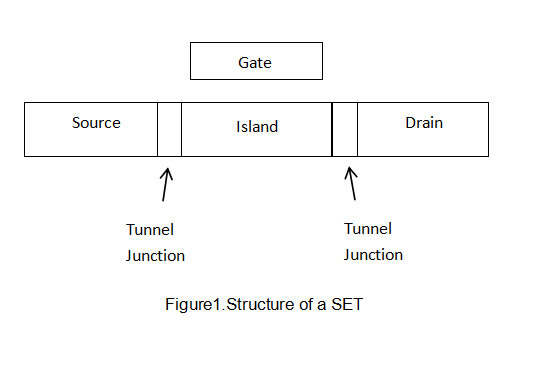
Figure 1: Structure of SET
2.2. Working principle of a single-electron transistor
The dimensions of conventional MOSFET are usually in the micron to nanometer scale. Although they are very small, they are still much larger than atomic and molecular sizes. Therefore, many of their properties can be described in macroscopic physics. For the SET, the size of the quantum island, one of the core parts, can be as small as a few nanometers to tens of nanometers. As quantum particles, electrons have wave-particle duality. At this very small size, electron volatility is more significant, causing electrons to behave differently than predicted by classical physics, making quantum effects more pronounced [4]. Quantum effects of a single-electron transistor (SET) usually include Coulomb blockade effect, quantum tunneling effect, quantum size effect.
2.2.1. Coulomb blockade effect
In nanostructures such as quantum dots, electrons are confined to a small space, which results in electrons being very close to each other and electronic states becoming more localized, increasing the possibility of overlapping electron clouds [5]. Therefore, the coulomb interaction between electrons at the nanoscale becomes very prominent and manifests as a repulsive force.
The Coulomb blockade effect is related to the coulomb interaction between electrons. When an electron attempts to enter or leave a nanoscale system, it must overcome an additional energy barrier caused by coulomb interactions with other electrons in the system, also known as charging energy Ec. In other words, due to the coulomb action, the addition of a single electron will change the total charge of the conductor, thereby increasing the total energy of the system, but because the system must follow the Law of Conservation of Energy, such a process is impossible, that is, only when the electron leaves the system after other electrons can enter the system.
\( Ec=\frac{{e^{2}}}{2C} \) (1)
From the expression of charging energy (1), it can be seen that charging energy is inversely proportional to capacitance. The quantum island capacitance of the nanoscale single-electron transistor (SET) is very small, and even the entry and exit of a single electron will form a large energy barrier, thus preventing other electrons from entering the quantum island. At this point, sufficient voltage can be applied to make other electrons gain enough energy to overcome this barrier [6].
This phenomenon of one electron tunneling into the quantum island will prevent the subsequent second electron from entering the quantum island is called the Coulomb blockade effect. Due to the Coulomb blockade effect, the conduction of a single-electron transistor (SET) involves only the transfer of a single electron.
2.2.2. Quantum tunneling effect
In quantum mechanics, microscopic particles can pass through a barrier higher than their own energy under certain conditions. This phenomenon is called quantum tunneling. The occurrence of this is related to the volatility of particles. It can be described by the wave function in the Schrodinger equation. When the wave function encounters a barrier, it does not suddenly drop to zero, but decays exponentially. This means that the particle has a certain probability of appearing on the other side of the barrier [7].
When Coulomb blockade occurs, the electrons cannot cross the energy barrier, and at this time the electrons cannot tunnel, that is, the single-electron transistor cutoff. Reducing the barrier or increasing the voltage so that the electrons have enough energy to tunnel the barrier, that is, single-electron transistor conduction. This reciprocation can control the transport of document making electrons.
2.2.3. Quantum size effect
When the size of a material is reduced to the nanoscale, its physical properties change significantly, which is called the quantum size effect. In a single-electron transistor, for example, quantum size effects cause the energy levels of electrons to become discrete, meaning that electrons can only exist at specific energy levels rather than being continuously distributed. This is based on the principles of quantum mechanics. When the size of the material is reduced to the nanoscale, the movement of the electrons is restricted, that is, the wave function of the electrons is spatially limited, and can only form be standing waves in a limited space. These standing waves correspond to specific energy states, so the energy levels become discrete [8].
This discrete energy level structure makes the transfer of electrons controllable, allowing a single-electron transistor (SET) to control current with the precision of a single electron.
2.3. Low-power analysis of a single-electron transistor
Because of the Coulomb blockade effect, single-electron transistors (SET) consume almost no power in the off state. In the conduction state, only one electron is transferred. Due to the quantum size effect, the electron energy level only takes a specific discrete value, and the electron only needs to obtain enough energy to jump to the next energy level to form a conductive channel. And this energy is far less than the energy required to move in the continuous energy range. Therefore, the threshold voltage of the device is very low, and only a very low voltage can realize the conduction of the device. The tunneling process requires no additional energy input. Therefore, single-electron transistors (SET) operate with very low power consumption due to the quantum effects.
3. Very low-power applications of quantum effects in single-electron transistors
Single-electron transistors (SET) are widely used in sensors, wearable devices, medical devices, quantum computing and other fields because of their low power consumption and high sensitivity. In this paper, the application of the low-power characteristics of single-electron transistors (SET) in the field of quantum computing is taken as an example, and compared with the application of MOSFET in the same aspect. The advantage of the ultra-low power of single-electron transistor (SET) is explained in detail.
3.1. Application of single-electron transistors in quantum computing
Single-electron transistors (SET) were first proposed for quantum computing in early 2000, but the technology was still immature at that time. With advances in nanomanufacturing technology, by 2018, research teams at IBM and Intel began testing single-electron transistors (SET) in quantum computers. In 2019, a research team at the Delft University of Technology in the Netherlands, led by renowned physicist Professor Lieven Vandersypen, began a study on the power consumption of single-electron transistors (SET) compared with MOSFET in quantum computing. Their experimental goals were to determine the difference in energy consumption between the two types of transistors for manipulating and reading qubits, and to analyze the advantages of single-electron transistors in quantum computing[9].
The experimental team integrated the single-electron transistors (SET) and MOSFET into two nearly identical quantum computing prototype systems, each for reading the state of silicon qubits. Both systems operate at temperatures close to absolute zero (about 20 mK), which is typical for quantum computing experiments [9].
The experimental results show that although the MOSFET can complete the qubit reading task, the energy consumption is high. In the experiment, the MOSFET consumes about 5nW of power each time the state of the qubit is read, and the noise problem is prominent when working at ultra-low temperatures, which affects the accuracy and stability of the read. In contrast, the power consumption of single-electron transistors (SET) is significantly reduced, consuming only about 0.1nW of power per reading qubit of state on average, which is about 50 times less power. Single-electron transistors (SET) are able to precisely control the transmission of individual electrons, ensuring high-precision qubit state reading and no significant noise interference at low temperatures [9].
3.2. Analysis of single-electron transistors for reducing noise and heat dissipation in quantum computing
In quantum computing, reading and manipulating qubits is the most energy-intensive and noisy part. Because this link needs to be carried out in an extremely refined and controlled environment, and requires complex quantum error correction technology, all of which make this link the most energy-consuming and the easiest part to introduce noise [10]. Single-electron transistors can significantly reduce power consumption through single-electron control and quantum tunneling effects and reduce heat dissipation and noise through the following principles.
In quantum computing, especially during the readout of qubits, the coulomb blockade effect of a single-electron transistor (SET) allows it to operate with extremely small currents while still being able to make highly accurate measurements of quantum states. This greatly reduces noise and heat dissipation due to the flow of many electrons.
Quantum tunneling is a heat-free process, so that electrons do not generate as much heat as traditional transmission during tunneling, so that the operation and measurement process of qubits can be carried out at extremely low temperatures to reduce thermal noise and maintain the coherence of the quantum state, without causing thermal disturbance to the system.
Traditional qubit readout circuits, especially those based on CMOS, usually require a high operating voltage, which is easy to produce electron migration and scattering effects, thus introducing noise. The quantum size effect makes the threshold voltage of a single-electron transistor very low, which means that when reading the qubit state, the circuit does not introduce noise due to high-voltage operation.
It can be seen that compared with traditional MOSFET, single-electron transistors (SET) not only have overwhelming advantages in power consumption, but also improve the reliability and stability of the system.
4. Conclusion
In this paper, the working principle of a single-electron transistor (SET) is explained by a series of quantum effects of it, and the reason of its very low power consumption is analyzed. By comparing its application with MOSFET in quantum computing, the paper analyzes the reason why the single-electron transistor (SET) can reduce noise and heat dissipation in quantum computing from the aspect of its working principle.
Despite the many advantages of single-electron transistors (SET), their current commercial application is still limited, mainly due to the complexity and cost of manufacturing technology. In terms of manufacturing accuracy, quantum dots and their associated structures need to be precisely manufactured at the nanoscale. Currently, although some advanced manufacturing processes such as lithography and electron beam lithography can achieve nanoscale accuracy, it is still difficult to maintain consistency and repeatability on the overall device. When it comes to manufacturing materials, single-electron transistors (SET) usually require special materials such as high-purity semiconductors or superconducting materials to efficiently capture and release electrons. The preparation and processing of these materials are very different from traditional silicon materials, and existing semiconductor processes are not necessarily compatible with these materials. Single-electron transistors (SET) rely on high-quality insulation to achieve quantum tunneling effects, and existing insulation materials may not provide sufficient performance, leading to leakage and loss of control of electrons.
The core of a single electron transistor is to control the behavior of a single electron, and this working mechanism determines that a single electron transistor usually needs to operate at a temperature close to absolute zero, and it is easy to be subjected to thermal disturbance in the room temperature environment and cause random movement of electrons. Similarly, single-electron transistors (SET) cannot be used for long periods of time.
To address the temperature limitations of single-electron transistors (SET), materials with higher electron mobility and low thermal noise, such as carbon nanotubes or graphene, can be used in the fabrication and design of single-electron transistor structures, which can improve performance at high temperatures. Using the spin of electrons rather than the charge for information processing can reduce the impact of temperature on device performance, while achieving higher integration and lower power consumption. By using quantum dot arrays or multi-island structures, the effect of temperature on the behavior of single electrons can be mitigated to a certain extent. This design allows electrons to be regulated across multiple islands, allowing for more efficient use of heat energy. Based on this, researchers have developed a variety of single-electron transistors (SET), such as multi-island single-electron transistors and graphene-based spin single-electron transistors. It is believed that in the future, single-electron transistors (SET) will overcome temperature and other limitations and be widely used.
References
[1]. Dixit, A. MOSFET on the Horizon: What's New and What's Next. IntechOpen. 2024.
[2]. Smith, J., & Zhang, L. (2020). Impact of Quantum Effects on the Performance of Sub-3nm MOSFETs. Journal of Applied Physics, 128(1), 011101.
[3]. Wang, Q., & Lee, H. J. (2010). Fabrication and Characterization of Single Electron Transistors. Journal of Applied Physics, 108(11), 114304.
[4]. Feynman, R. (2019). The Wave-Particle Duality of Electrons. Physical Review Letters, 122(5), 045001.
[5]. Wang, L., & Zhang, Y. (2021). Electron correlation and quantum localization in nano-scale systems. Journal of Physical Chemistry C, 125(30), 16234-16240.
[6]. K. S. P. Rao, K. N. M. Rao, and M. R. Jaya Surya, "Single-electron transistors: From theory to applications," Materials Science in Semiconductor Processing, vol. 118, pp. 109-118, 2020.
[7]. C. M. Bender and D. W. Hook, "Quantum tunneling as a classical anomaly," Journal of Physics A: Mathematical and Theoretical, vol. 44, no. 37, pp. 372001, 2011.
[8]. J. Ahn, J. Park, S. Lee, et al., "Quantum-size effects in sub 10-nm fin width InGaAs FinFETs," in Proc. 2016 IEEE Int. Electron Devices Meeting (IEDM), 2016, pp. 28.5.1-28.5.4.
[9]. L.Vandersypen et al., "A coherent spin–qubit system in silicon," Nature Electronics, 2020.
[10]. Konrad M. et al., "Single-Electron Transistor as a Charge Sensor for Qubits," Applied Physics Letters, 2019.
Cite this article
Wang,Q. (2025). Application of the Quantum Effects of Single-Electron Transistors in Low-power. Applied and Computational Engineering,130,102-107.
Data availability
The datasets used and/or analyzed during the current study will be available from the authors upon reasonable request.
Disclaimer/Publisher's Note
The statements, opinions and data contained in all publications are solely those of the individual author(s) and contributor(s) and not of EWA Publishing and/or the editor(s). EWA Publishing and/or the editor(s) disclaim responsibility for any injury to people or property resulting from any ideas, methods, instructions or products referred to in the content.
About volume
Volume title: Proceedings of the 5th International Conference on Materials Chemistry and Environmental Engineering
© 2024 by the author(s). Licensee EWA Publishing, Oxford, UK. This article is an open access article distributed under the terms and
conditions of the Creative Commons Attribution (CC BY) license. Authors who
publish this series agree to the following terms:
1. Authors retain copyright and grant the series right of first publication with the work simultaneously licensed under a Creative Commons
Attribution License that allows others to share the work with an acknowledgment of the work's authorship and initial publication in this
series.
2. Authors are able to enter into separate, additional contractual arrangements for the non-exclusive distribution of the series's published
version of the work (e.g., post it to an institutional repository or publish it in a book), with an acknowledgment of its initial
publication in this series.
3. Authors are permitted and encouraged to post their work online (e.g., in institutional repositories or on their website) prior to and
during the submission process, as it can lead to productive exchanges, as well as earlier and greater citation of published work (See
Open access policy for details).
References
[1]. Dixit, A. MOSFET on the Horizon: What's New and What's Next. IntechOpen. 2024.
[2]. Smith, J., & Zhang, L. (2020). Impact of Quantum Effects on the Performance of Sub-3nm MOSFETs. Journal of Applied Physics, 128(1), 011101.
[3]. Wang, Q., & Lee, H. J. (2010). Fabrication and Characterization of Single Electron Transistors. Journal of Applied Physics, 108(11), 114304.
[4]. Feynman, R. (2019). The Wave-Particle Duality of Electrons. Physical Review Letters, 122(5), 045001.
[5]. Wang, L., & Zhang, Y. (2021). Electron correlation and quantum localization in nano-scale systems. Journal of Physical Chemistry C, 125(30), 16234-16240.
[6]. K. S. P. Rao, K. N. M. Rao, and M. R. Jaya Surya, "Single-electron transistors: From theory to applications," Materials Science in Semiconductor Processing, vol. 118, pp. 109-118, 2020.
[7]. C. M. Bender and D. W. Hook, "Quantum tunneling as a classical anomaly," Journal of Physics A: Mathematical and Theoretical, vol. 44, no. 37, pp. 372001, 2011.
[8]. J. Ahn, J. Park, S. Lee, et al., "Quantum-size effects in sub 10-nm fin width InGaAs FinFETs," in Proc. 2016 IEEE Int. Electron Devices Meeting (IEDM), 2016, pp. 28.5.1-28.5.4.
[9]. L.Vandersypen et al., "A coherent spin–qubit system in silicon," Nature Electronics, 2020.
[10]. Konrad M. et al., "Single-Electron Transistor as a Charge Sensor for Qubits," Applied Physics Letters, 2019.