


1. Introduction
Transconductance amplifiers have been around for a long time, but with the development of technology, many kinds of transconductance amplifiers have been derived. The structures of similar amplifiers are constantly being updated and improved, leading to their application in many different fields. Krishna, M. and Nagar, B.C mentioned that as Complementary Metal Oxide Semiconductor (CMOS) devices tend to become smaller, the proportion of integrated circuits is also shrinking. This trend creates a growing demand for active elements used in analog signal processing that require low power consumption and low supply voltage [1]. When traditional operational amplifiers cannot meet these requirements, attention shifts to newer differential transconductance amplifiers [2]. Currently, some researchers have used these differential transconductance amplifiers to meet the demand for filters with lower power consumption and smaller area, achieving the advantages of wide areas and low power consumption [2-3].
This article reviews several types of differential transconductance amplifiers that aim to meet the increasing demands for low power consumption and compact size in modern applications. Specifically, it focuses on Voltage Differential Transconductance Amplifiers (VDTA) and Current Differential Transconductance Amplifiers (CDTA), exploring their various application fields. This research provides scholars with detailed information about different types of differential transconductance amplifiers and facilitates a clearer grasp of the technology and its potential uses.
2. Differential Transconductance Amplifier
The features and advantages of the two differential amplifiers, VDTA and CDTA, are briefly described.
The VDTA operates on the principle of converting the voltage difference between the two inputs into a transconductance value. The transconductance value is then used to generate the output current [4]. The primary advantage of VDTA lies in its ability to integrate voltage-to-current conversion into a single stage, thereby simplifying circuit design [5]. Active power filter is one of the important building blocks [2, 6]. The CDTA is a kind of pure current mode multifunctional device. It accepts current as an input and produces it again as an output [7]. The advantage is that the output gain can be adjusted with the help of the transconductance value, and this transconductance value can be used to control various parameters in any circuit [8]. It is widely used in biomedical signal processing, low-frequency filtering and neural network computing [8-9].
2.1. Voltage Difference Transconductance Amplifier
2.1.1. Filters
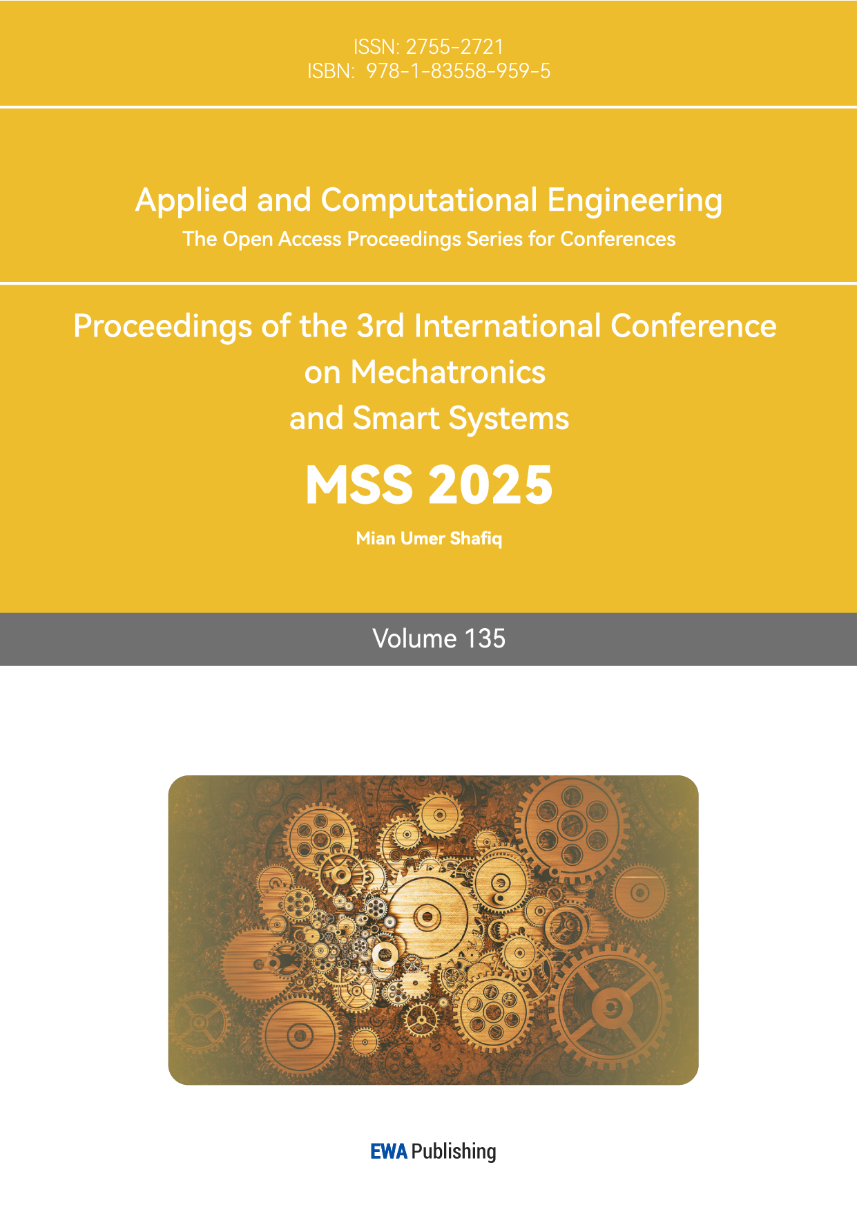
D. Shukla and S. Tripathi [2] tuneable universal filters designed by VDTA are bandpass, low-pass, and high-pass filters based on a single VDTA, operated by three capacitors and an active resistor. However, it is worth noting that the active resistance is realized by N-type Metal-Oxide-Semiconductor (NMOS) transistors. Through their circuit simulation, they found that the filter design of this VDTA meets the requirements of low power consumption and compact CMOS implementation. The practice of replacing passive resistance with NMOS active resistance can reduce the area occupancy, and the active resistance filter has a high noise resistance and it also provides the tuning ability for the filter.
The specific working principle is that \( p \) and \( n \) are voltage inputs, and \( x+ \) and \( x- \) are current inputs. It has input and output transconductance stages. The input transconductance stage converts the differential input voltage (VP−VN) into the current \( \) IZ, and the output transconductance stage converts the voltage VZ at the terminal \( z \) into the current IX. And all terminals of the VDTA have high impedance values. The relationship between voltage and current is shown in (1) [6].
\( (\begin{matrix}{I_{Z}} \\ {I_{X-}} \\ {I_{X+}} \\ \end{matrix})=(\begin{matrix}{g_{m1}} & -{g_{m1}} & & & 0 \\ 0 & & 0 & & -{g_{m2}} \\ 0 & & 0 & & {g_{m2}} \\ \end{matrix})(\begin{matrix}{V_{P}} \\ {V_{N}} \\ {V_{Z}} \\ \end{matrix}) \) (1)
Figure 1 is a picture of VDTA circuit.
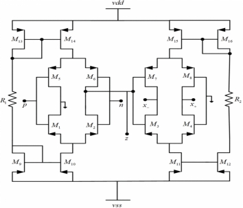
Figure 1: CMOS implementation of VDTA [2].
Similarly, S. Singh, Garima, and B. Jaint used VDTA to design filters. However, they used two VDTAs and two ground capacitors to form the biquad filter [6]. The previous filter utilizes a single VDTA. The VDTA construction and working principle of the two are the same. However, compared with the above filters, the dual-mode SIMO biquad filter has a wider range of application scenarios, and can realize a variety of filtering functions in different modes. For example, the current and cross-pass mode can provide low-pass, high-pass and band-pass mode functions, while the voltage mode can provide low-pass and band-pass mode functions. Moreover, because it is composed of two VDTAs, the angular frequency and bandwidth can be tuned independently, allowing for greater flexibility and practicality without affecting each other's performance. Figure 2 is an image of this filter.
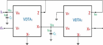
Figure 2: Dual mode SIMO biquad filter [6].
2.1.2. Four-quadrant Multiplier/Divider
The application of VDTA is not only in the filter but also in the voltage difference transconductance amplifier (VDTA) as the active component of the four-quadrant multiplier/divider circuit. Simultaneous current mode multipliers/dividers are considered an important design, especially in neural activity modeling for neuromorphic computing applications.
Krishna, M. and Nagar, B.C also used Dynamic Threshold Metal Oxide Semiconductor (DTMOS) technology in this circuit. DTMOS technology offers several advantages such as low power consumption, strong current drive capability, high transconductance, low leakage power, and minimized parasitic capacitance. This technology is specifically embodied in the DTMOS transistor, where both the body terminal and the gate terminal are connected together to reduce the leakage current and improve the multiplier circuit. This setup allows the circuit to operate at low supply voltages with high current drive and minimal history effects, thereby reducing leakage power consumption [1]. The structure and operating principle of VDTA remain as described above, but this circuit not only focuses on VDTA and combines it with other technologies. Additionally, no external resistors or capacitors are required in the circuit design, so it can reduce circuit complexity and temperature sensitivity.
Figure 3 is the detailed structure of this four-quadrant multiplier/divider with VDTA. The multiplication operation is performed by keeping (Z1−Z2) constant, and the output voltage Vo is obtained by multiplying the input signal (X1−X2) and (Y1−Y2). Division operation is by keeping (X1 - X2) (X1 - X2) is constant, the input signal (Y1 - Y2) divided by (Z1 - Z2) to obtain the output voltage Vo [1].
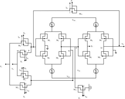
Figure 3: DTMOS-based four quadrant multiplier/divider with VDTA [1].
VDTA has many different applications now because of its unique advantages. What this article introduces is only a small part of its application. CDTA also has its own advantages, the difference between the two is that CDTA is a pure current mode rather than voltage mode of multifunctional devices, often designed for low power and high frequency applications.
2.2. Current Difference Transconductance Amplifier
2.2.1. Modulator
N. Pandey et al. designed a versatile modulator using CDTAs [3]. Modulators are widely used in communication systems because they help minimize the effects of noise and move the spectrum of the modulated signal into a frequency range consistent with the transmission system. Modulation also reduces interference because users can provide carrier signals with different frequencies for different message signals with the same frequency. CDTA has no parasitic capacitance; its current mode operation makes it possible to work in a wide frequency range. It includes a current differencer (formed by transistors Mc1-Mc17) controlled by the input current difference and a transconductance amplifier (formed by transistors Mc18-Mc26, converting the current difference into an output current, with its transconductance gain controlled by the bias current IBias). At the same time, the use of the proposed CDTA multi-function modulator circuit with large bandwidth, low power consumption and the use of the intrinsic carrier signal.
The modulator operates based on a pulse generator circuit constructed using CDTA modules. Initially, the first CDTA stage functions as an integrator, causing the output voltage Vz to change linearly with time. Subsequently, the second CDTA stage, along with resistors, forms a Schmitt trigger. When the output voltage of the integrator reaches a predetermined threshold, the output voltage of the Schmitt trigger flips, resulting in stable switching behavior. The third CDTA stage acts as a constant current source, supplying the first CDTA with a constant positive or negative current based on the output state of the second CDTA. This switching of current controls the charging and discharging process of the integrator, enabling the circuit to generate continuous periodic oscillations. Through this design, the pulse generator effectively produces the necessary modulation signal, providing a stable carrier signal for the subsequent modulation process [3].
Their research led to multifunctional modulators that can be used as AM, FM, Delta, and Sigma Delta modulators. And CDTA-based AM and FM modulators proved to be the most ideal in terms of power consumption, while CDTA-based Delta modulators appeared to be optimal in terms of output noise voltage. The signal-to-noise ratio is the largest in amplitude modulation and the smallest in Sigma Delta modulation [3].
CDTA circuit and pulse generator diagram is shown in Figure 4 and 5.
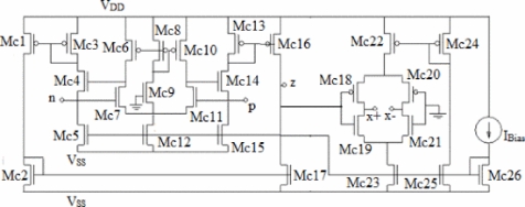
Figure 4: CMOS implementation of CDTA [3].
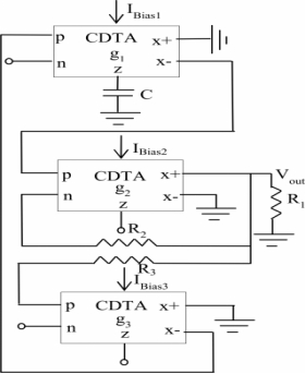
Figure 5: CDTA based pulse generator circuit [3].
2.2.2. Biomedical Signal Processing
The low-transconductance M-CDTA design proposed by Gangal, V. Bhanoo and N. Pandey used in biomedical signal processing [9]. They replaced the load transistors in the conventional CDTA with N parallel PMOS transistors so it can reduce the transconductance to 1/N of the original. The circuit is designed in 180nm CMOS technology and verified by Cadence Virtuoso simulation.
The CDTA here works similarly to the above, also consisting of a current-differential unit (CDU) and a transconductance amplifier (TA) with input currents Ip and In, which flow into the p and n terminals of the CDU, respectively. The output current \( Iz =Ip - In \) , and then into TA, TA converts this current into voltage \( Vz \) and then into current \( Ix \) , the output current is proportional to \( Vz \) , the relationship is \( Ix = gmVz \) . In Figure 6, red \( N \) shows the load transistors replaced by \( N \) parallel PMOS transistors.
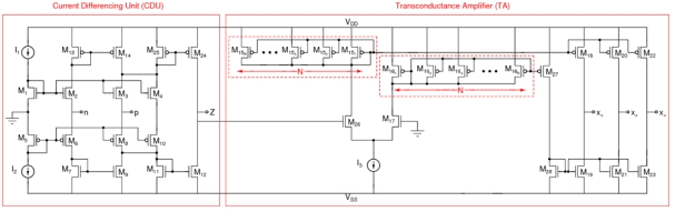
Figure 6: Low-transconductance M - CDTA CMOS implementation [9]
In order to verify the performance of M-CDTA, a low frequency current mode filter is designed. The filter consists of two M-CDTA modules and two ground capacitors (C1 and C2), as shown in Figure 7.
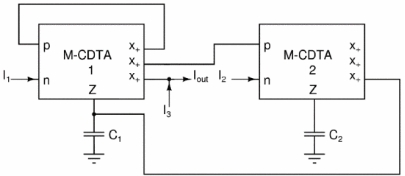
Figure 7: Low frequency filter [9].
This M-CDTA-based filter processes signals using two M-CDTA units and two grounded capacitors. The filter type is determined by different combinations of input currents. The core of the filter lies in the M-CDTA units, which perform current differencing and transconductance amplification to achieve signal conversion and processing. The pole frequency of the filter is jointly determined by the transconductance value and capacitance, while electronic tuning is enabled by adjusting the transconductance via the bias current IBias. Additionally, the capacitance ratio influences the bandwidth and quality factor, allowing flexible adjustment of the frequency response characteristics of the filter [9].
The low transconductance M-CDTA module proposed by them realizes the low transconductance characteristics through current shunt technology, and has been successfully applied to the general low-frequency filter in biomedical signal processing. The filter has the advantages of low power consumption and low noise and is suitable for portable and implantable medical devices [9].
2.3. CDTA Combined with VDTA
2.3.1. Grounded Flux Controlled Meminductor
VDTA and CDTA can also form a Grounded Flux-Controlled Meminductor by R. Das, S. Karmakar, A. Banerjee and S. K. Shaw [10]. A low-complexity meminductor (Meminductor) design scheme is proposed. This circuit uses only one VDTA, one CDTA, and two capacitors to achieve both incremental and decremental operating modes, making it suitable for low-frequency signal processing. Meminductor, as an extension of the memristor and memcapacitor, is an electronic component with memory characteristics that can adjust its inductance based on previous current or voltage changes. Due to its unique memory properties, meminductors have a wide range of application prospects in fields such as neural networks, analog circuits, non-volatile memory, and neuromorphic computing.
Circuit Design and Working Principle: The circuit structure is shown in Figure 8 The VDTA receives the input voltage signal and converts it into a current signal through its differential input terminals (P and N), which is then stored in capacitor C1. The CDTA receives the current signal from the VDTA and mirrors it to the output terminal through a current mirror. Capacitor C2 is used to store the output current signal.
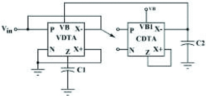
Figure 8: Meminductor Circuit Diagram [10]
Their simulations were conducted using the 180nm TSMC process to verify the circuit's performance. The shape and area of the PHL remain stable across different frequencies and capacitance values, indicating that the circuit has good stability. The flux voltage remains stable even after the input pulse signal is removed, verifying the non-volatility characteristic. With a 5% deviation in capacitance values and bias currents, the pole frequency of the circuit changes by 9.87% and 9.32%, respectively, demonstrating good stability [10].
The meminductor circuit designed by R. Das, S. Karmakar, A. Banerjee and S. K. Shaw has the advantages of low complexity, electronic tunability, and non-volatility. The simulation results validate its effectiveness and reliability, indicating that the circuit has broad application prospects in the field of meminductor applications [10].
3. Possible Drawbacks
Although VDTA and CDTA have many advantages and have a wide range of applications, it is essential to recognize that each technology has its limitations. For example, while improving performance in one area, CDTA may reduce capacities in others. If it increases transconductance, it reduces bandwidth. As a result, some types of CDTA are most suitable for low-voltage, low-power applications, such as biomedical pacemakers, but may not be suitable for high-frequency applications [7]. For VDTA, achieving a higher transconductance gain when MOS transistors are saturated is crucial for its functional realization [3]. Meanwhile, the current characteristics in the saturated region are more stable, which is conducive to the realization of high linearity and low distortion [6]. Therefore, the application of VDTA is also subject to specific limitations.
4. Conclusion
In summary, both voltage and current differencing transconductance amplifiers (VDTA and CDTA) have a wide range of applications and represent relatively new technologies. This paper reviews their roles as key components in various architectures, such as filters, four-quadrant multipliers/dividers, modulators, biomedical signal processors, and grounded flux-controlled meminductors. The characteristics and advantages of both are highlighted. VDTAs offer compact size and low power consumption, while CDTAs enable adjustable output gain via transconductance (gₘ), with this transconductance further serving to control diverse parameters in circuits. It is hoped that this review will help readers better grasp the principles and practical applications of these amplifiers, inspiring future research ideas in the field.
However, it is a pity that this article has not conducted actual research and simulation, lacking specific experimental research data. Additionally, many different kinds of differential transconductance amplifiers are not mentioned in this paper and various application areas are not comprehensively covered.
Although the differential transconductance amplifier still needs to be improved, its future is very promising. As mentioned above, it can be used in the optimization and construction of neural networks, potentially reducing the power consumption of AI operations. This could lead to training AI models requiring significantly less power than currently needed. Perhaps in the future, there will be hearing aids, wearable devices, and pacemakers with improved user experiences. These devices require signal processing circuits that are low-power, low-noise, and high-gain. The components described in this paper can meet these requirements. As the technology matures, it will make human’s lives more convenient.
References
[1]. Krishna, M., Nagar, B.C. (2024). DTMOS based four-quadrant multiplier/divider with voltage difference transconductance amplifier. Analog Integr Circ Sig Process, 118, 371–386.
[2]. D. Shukla, S. Tripathi. (2020). Design of VDTA based tuneable universal filters. 2020 IEEE Students Conference on Engineering & Systems (SCES). Prayagraj, India, pp. 1-3.
[3]. N. Pandey, A. Sayal, M. Tripathi and R. Pandey. (2013). Design of versatile modulator using CDTAs. 2013 International Conference on Emerging Trends in Communication, Control, Signal Processing and Computing Applications (C2SPCA). Bangalore, India, pp. 1-6.
[4]. Babu, E.V., et al. (2023). Design and Implementation of Voltage Difference Transconductance Amplifier. 2023 3rd International Conference on Mobile Networks and Wireless Communications (ICMNWC), Mobile Networks and Wireless Communications (ICMNWC), 2023 3rd International Conference on, pp. 1–5.
[5]. MAHENDRA, M., KUMARI, S., GUPTA, M. (2023). DTMOS Based Low Power Adaptively Biased Fully Differential Transconductance Amplifier with Enhanced Slew-Rate and its Filter Application. IETE Journal of Research, 69(6), 3288–3307.
[6]. S. Singh, Garima and B. Jaint. (2024). Dual Mode SIMO Biquad Filter Using VDTA. 2024 International Conference on Electronics, Computing, Communication and Control Technology (ICECCC), Bengaluru, India, pp. 1-6.
[7]. Bisariya, S., Afzal, N. (2020). Design and implementation of CDTA: a review. Sādhanā: Published by the Indian Academy of Sciences, (45) 1.
[8]. A. Gangal, V. Bhanoo and N. Pandey. (2020). Low Transconductance M-CDTA Block and its Application in Biomedical Signal Processing," 2020 International Conference on Electronics and Sustainable Communication Systems (ICESC), Coimbatore, India, pp. 1101-1107.
[9]. R. Das, S. Karmakar, A. Banerjee and S. K. Shaw. (2024). VDTA and CDTA based Grounded Flux Controlled Meminductor. 2024 IEEE International Conference on Communication, Computing and Signal Processing (IICCCS), ASANSOL, India, pp. 1-6.
Cite this article
Yan,H. (2025). Difference Transconductance Amplifiers and Their Applications. Applied and Computational Engineering,135,132-139.
Data availability
The datasets used and/or analyzed during the current study will be available from the authors upon reasonable request.
Disclaimer/Publisher's Note
The statements, opinions and data contained in all publications are solely those of the individual author(s) and contributor(s) and not of EWA Publishing and/or the editor(s). EWA Publishing and/or the editor(s) disclaim responsibility for any injury to people or property resulting from any ideas, methods, instructions or products referred to in the content.
About volume
Volume title: Proceedings of the 3rd International Conference on Mechatronics and Smart Systems
© 2024 by the author(s). Licensee EWA Publishing, Oxford, UK. This article is an open access article distributed under the terms and
conditions of the Creative Commons Attribution (CC BY) license. Authors who
publish this series agree to the following terms:
1. Authors retain copyright and grant the series right of first publication with the work simultaneously licensed under a Creative Commons
Attribution License that allows others to share the work with an acknowledgment of the work's authorship and initial publication in this
series.
2. Authors are able to enter into separate, additional contractual arrangements for the non-exclusive distribution of the series's published
version of the work (e.g., post it to an institutional repository or publish it in a book), with an acknowledgment of its initial
publication in this series.
3. Authors are permitted and encouraged to post their work online (e.g., in institutional repositories or on their website) prior to and
during the submission process, as it can lead to productive exchanges, as well as earlier and greater citation of published work (See
Open access policy for details).
References
[1]. Krishna, M., Nagar, B.C. (2024). DTMOS based four-quadrant multiplier/divider with voltage difference transconductance amplifier. Analog Integr Circ Sig Process, 118, 371–386.
[2]. D. Shukla, S. Tripathi. (2020). Design of VDTA based tuneable universal filters. 2020 IEEE Students Conference on Engineering & Systems (SCES). Prayagraj, India, pp. 1-3.
[3]. N. Pandey, A. Sayal, M. Tripathi and R. Pandey. (2013). Design of versatile modulator using CDTAs. 2013 International Conference on Emerging Trends in Communication, Control, Signal Processing and Computing Applications (C2SPCA). Bangalore, India, pp. 1-6.
[4]. Babu, E.V., et al. (2023). Design and Implementation of Voltage Difference Transconductance Amplifier. 2023 3rd International Conference on Mobile Networks and Wireless Communications (ICMNWC), Mobile Networks and Wireless Communications (ICMNWC), 2023 3rd International Conference on, pp. 1–5.
[5]. MAHENDRA, M., KUMARI, S., GUPTA, M. (2023). DTMOS Based Low Power Adaptively Biased Fully Differential Transconductance Amplifier with Enhanced Slew-Rate and its Filter Application. IETE Journal of Research, 69(6), 3288–3307.
[6]. S. Singh, Garima and B. Jaint. (2024). Dual Mode SIMO Biquad Filter Using VDTA. 2024 International Conference on Electronics, Computing, Communication and Control Technology (ICECCC), Bengaluru, India, pp. 1-6.
[7]. Bisariya, S., Afzal, N. (2020). Design and implementation of CDTA: a review. Sādhanā: Published by the Indian Academy of Sciences, (45) 1.
[8]. A. Gangal, V. Bhanoo and N. Pandey. (2020). Low Transconductance M-CDTA Block and its Application in Biomedical Signal Processing," 2020 International Conference on Electronics and Sustainable Communication Systems (ICESC), Coimbatore, India, pp. 1101-1107.
[9]. R. Das, S. Karmakar, A. Banerjee and S. K. Shaw. (2024). VDTA and CDTA based Grounded Flux Controlled Meminductor. 2024 IEEE International Conference on Communication, Computing and Signal Processing (IICCCS), ASANSOL, India, pp. 1-6.