


1. Introduction
Ga2O3 LDMOSFET is a power device in which all electrodes are located on the device surface, resulting in lateral carrier transport during operation. Owing to its ease of fabrication and seamless integration into power integrated circuits, the Ga2O3 LDMOSFET has attracted significant attention in recent years. Research has primarily focused on the N-channel β-Ga2O3 LDMOSFET, which features a negative threshold voltage; by applying a sufficiently negative bias to the gate, a depletion region is formed that effectively pinches off the conductive channel, thereby turning off the device[1].
In 2012, the Higashiwaki group at Japan’s NICT successfully demonstrated the first Sn-doped N-channel β-Ga2O3 MESFET (see Figure 1)[2]. Building on this work, in 2013 Higashiwaki et al. introduced a basic depletion-mode β-Ga2O3 LDMOSFET with a threshold voltage (Vth) of -15 V, a breakdown voltage of 370 V, and an on/off current ratio exceeding 10¹⁰[3]. In 2016, Wong and colleagues proposed the first depletion-mode β-Ga2O3 LDMOSFET with an integrated field plate. This design was realized by epitaxially growing on an unintentionally doped (UID) Ga2O3 buffer layer and employing multi-step silicon ion implantation to form a box-like N-type channel along with heavily doped N+ source and drain regions[4]. In 2017, Chabak et al. introduced an enhancement-mode β-Ga2O3 LDMOSFET featuring a trench gate structure, which achieved a threshold voltage of 3 V, an on/off current ratio over 10⁹, and a breakdown voltage of 505 V[5]. The following year, Zeng et al. improved upon the gate field plate design by dividing the underlying dielectric layer into two parts: a 50 nm high-quality SiO₂ layer deposited via atomic layer deposition (ALD) and a 350 nm SiO₂ layer deposited by plasma-enhanced chemical vapor deposition (PECVD)[6]. In 2022, Sharma et al. further refined the gate field plate dielectric by replacing the conventional dielectric with a polymer passivation layer[7], while Wang et al. presented the first lateral superjunction β-Ga2O3 LDMOSFET (see Figure 2)[8].
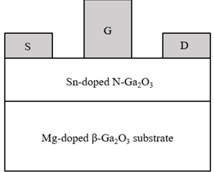
Figure 1: Sn-doped N-channel β-Ga2O3 MESFET Device[2]
Figure 2: Lateral Superjunction β-Ga2O3 LDMOSFET Device[8]
Despite these advances, studies on the thermal effects and the impact of bulk defects on β-Ga₂O₃ MOSFET performance remain limited—especially concerning device behavior under high-temperature conditions and the influence of bulk defects on off-state characteristics. In this work, we employ SENTAURUS TCAD simulation software to systematically investigate the static characteristics, thermal effects, and the influence of bulk defects in β-Ga₂O₃ MOSFETs.
In this paper, section 1 illustrates the application scenarios of power devices, the material properties of Ga₂O₃, and the development history and current status of Ga₂O₃ power devices, with a focus on lateral Ga₂O₃ LDMOSFETs. Section 2 details the structure, parameters, and physical models used in the simulations of Ga₂O₃ devices. Section 3 analyzes the basic static characteristics of the device, including its transfer and output characteristics, and introduces an avalanche model to extract key performance parameters from its breakdown behavior. Section 4 incorporates a thermal model to compare the transfer characteristics at 300 K and 600 K, thereby exploring the effects of temperature on the threshold voltage and leakage current. Finally, the influence of bulk defects on the device is examined by analyzing how variations in trap charge concentration affect the conduction state in the off condition.
2. Structure and Simulation
In this section, a simple β-Ga₂O₃ LDMOSFET device structure is constructed(see figure 3). The structure is based on a p-type Ga₂O₃ substrate, on which an n-type Ga₂O₃ drift region is formed, followed by the sequential definition of heavily doped source and drain regions on the n-type region. An insulating layer of Al₂O₃ is then deposited above the n-type region, with the gate metal subsequently deposited on top of the Al₂O₃. A highly doped n⁺⁺ β-Ga₂O₃ region with a doping concentration of 3×10¹⁹ cm⁻³ is introduced beneath the contacts in order to reduce the contact resistance. A 20 nm thick Al₂O₃ layer is implemented as the gate dielectric. In the simulated structure, the source-to-drain spacing is set at 30 µm, the gate length at 2 µm, and the gate width at 20 µm, while the thickness of the ungated β-Ga₂O₃ channel region is defined as 0.3 µm to further optimize device performance.
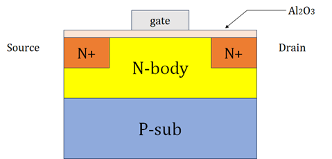
Figure 3: Ga2O3 MOSFET structure used in the simulation
For the simulation of basic static characteristics, the OldSlotboom bandgap narrowing model is employed to account for the intrinsic carrier concentration, which is influenced by the semiconductor’s bandgap and the states density at the band edges; additionally, a doping-dependent Shockley-Read-Hall (SRH) recombination model is used to describe carrier generation and recombination processes, emphasizing the impact of doping concentration on carrier lifetime. To simulate the breakdown characteristics, an avalanche model is incorporated on top of the SRH model, thereby simultaneously considering SRH recombination and avalanche breakdown effects. In order to achieve higher simulation accuracy, the transient scan algorithm is replaced by a quasi-static scan algorithm. Furthermore, given the significant impact of self-heating effects on the electrical characteristics of power devices with large active areas, high current densities, and high power densities, a thermodynamic model is also included in the simulation. The parameters used in the Ga₂O₃ device simulation are provided in Table 1.
3. The static performance Simulation
To analyze the static performance of the β-Ga₂O₃ MOSFET, simulations were performed using Sentaurus TCAD, from which the transfer, output, and breakdown characteristic curves were extracted.
Table 1: β − Ga2O3- Parameters
Parameter | Gallium Oxide | Units |
Band Gap | 4.6 | eV |
Critical breakdown electric field | 8 | MV/cm |
Dielectric Constant | 10.0 | N/A |
Electron Mobility | 300 | cm²/V·s |
Electron Affinity | 4.0 | eV |
3.1. The transfer characteristics
Figure 4 presents the transfer characteristics: under a fixed source-drain voltage of 1V, the gate voltage was incrementally scanned to observe the device’s on/off behavior. The results indicate that when the gate voltage becomes more negative, the drain current (Id) remains extremely low, signifying that the device is in the off state; as the gate voltage increases to approximately -3.5V, the drain current rises significantly, indicating that the device enters the on state; further increases in Vg cause Id to grow exponentially. This behavior suggests that the device’s threshold voltage (Vth) is around -3.5V, consistent with the characteristics of a depletion-mode (D-mode) MOSFET. However, the current simulation does not include the effects of interface roughness scattering, gate oxide interface traps, fixed interface charges, or bulk defect models, which may affect the accurate simulation of mobility variations[9].
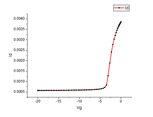
Figure 4: the transfer characteristic curve
3.2. The output characteristics
Figure 5 illustrates the output characteristics of the β-Ga₂O₃ MOSFET, specifically the variation of the drain current (Id) with the drain voltage (Vd). As observed in Figure 5, in the low Vd region, Id increases approximately linearly, indicating that the device operates in the linear region. In this region, the carriers in the MOSFET channel are driven by the source-to-drain voltage, and the current is mainly controlled by the channel resistance Rds(on), resulting in an approximately linear relationship between Id and Vd. The current can be approximately expressed as:
\( {I_{D}}≈{μ_{n}}{C_{ox}}\frac{W}{L}({V_{G}}-{V_{th}}-\frac{{V_{D}}}{2}){V_{D}} \ \ \ (1) \)
Where W/L is the channel width-to-length ratio, Cox is the gate oxide capacitance, μn is the electron mobility, Vg is the gate voltage, and Vth is the threshold voltage. In this region, the device current is primarily determined by the channel’s conductive properties, and the on-resistance can be estimated from the slope of the linear region; a lower on-resistance implies lower power consumption, which is advantageous for efficient power electronic applications.
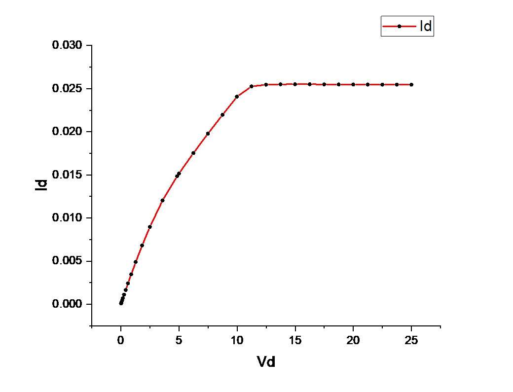
Figure 5: the output characteristic curve
As Vd increases to approximately 10 V, the rate of increase of Id gradually diminishes and eventually saturates, indicating that the MOSFET has entered the saturation region. At this stage, the carrier velocity in the channel reaches saturation, so that further increases in Vd do not lead to a significant increase in current; the saturation current can be approximated by:
\( {I_{D}}≈\frac{1}{2}{μ_{n}}{C_{ox}}\frac{W}{L}{({V_{G}}-{V_{th}})^{2}}\ \ \ (2) \)
In the saturation region, the current is primarily limited by the velocity saturation of the carriers, causing Id to remain almost constant with further increases in Vd. This characteristic is particularly important for power devices as it determines the maximum current carrying capability of the MOSFET. Moreover, for β-Ga₂O₃ MOSFETs—being wide bandgap semiconductor devices—the high breakdown electric field (approximately 8 MV/cm) enables operation at higher voltages; however, the relatively low thermal conductivity may lead to self-heating effects, potentially affecting the long-term stability of the device.
3.3. The breakdown characteristics
As introduced earlier, owing to the 4.6 eV bandgap, Ga₂O₃’s excellent voltage withstand capability has attracted significant attention. In simulations of the βGa₂O₃ MOSFET structure, breakdown occurs mainly in two regions: source–drain lateral breakdown and gate breakdown[10].
Source–Drain Breakdown: Source–drain breakdown refers to the phenomenon in which, under the condition that the device channel is off, a reverse voltage is applied between the source and drain and gradually increased. When the voltage reaches a certain value, the gate’s barrier effect weakens, leading to a sudden jump in current that forms a closed loop between the source and drain. Internationally, the voltage at which the reverse current reaches 1 mA/mm is defined as the breakdown voltage. This process is typically called “soft breakdown” because the device is not physically damaged—only its characteristics are altered. Under test conditions, the breakdown voltage determined from the soft breakdown test result is taken as the actual breakdown voltage of the device. the static performance.
Gate Breakdown:Gate breakdown is caused by leakage current induced by the reverse bias of the Schottky gate. Some reports suggest that when the device operates at a high drain voltage, the presence of defects or surface states prevents the gate’s Schottky contact from acting as an ideal unidirectional conductor. As a result, a small portion of electrons may leak out from the gate, generating gate leakage current. When this gate leakage current reaches 1 mA/mm before the source–drain current does, a closed loop is formed between the source and the gate.
According to breakdown characteristics presented in this paper, the gate voltage (Vg) is fixed at -10 V to ensure that the device is completely turned off. Then, the drain–source voltage (Vd) is gradually increased while observing the change in drain current (Id). The simulation results are shown in Figure 6.
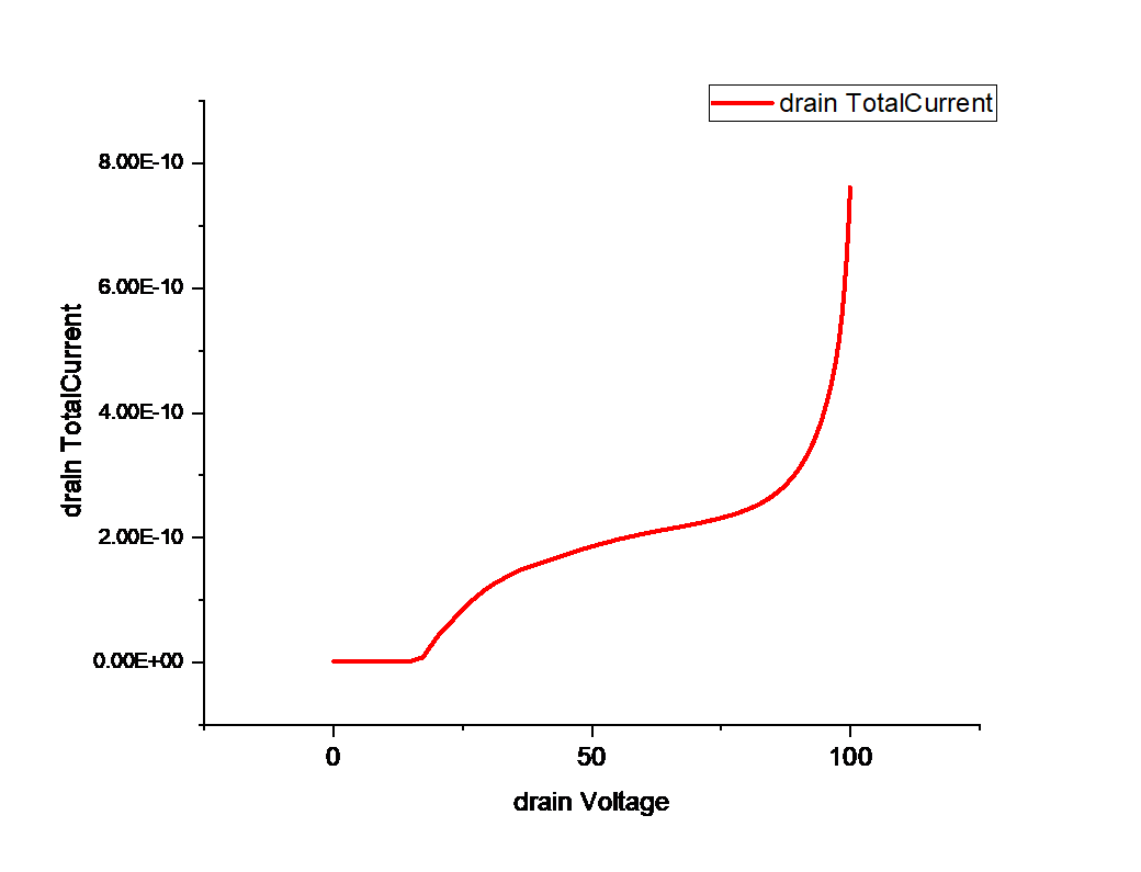
Figure 6: the breakdown characteristic curve
It can be seen that when Vd is in a relatively low range, the device’s drain current remains extremely low (< 10⁻¹⁰ A), indicating that the device is off—this shows that under low electric field conditions, there are very few carriers in the channel, resulting in almost no leakage current. When Vd increases to around 100 V, the drain current exhibits an exponential increase, indicating that 100V has reached the breakdown voltage(BV) of the β‑Ga₂O₃ MOSFET.
4. Temperature Characteristics Simulation
The majority of power dissipation in high-voltage devices occurs within the channel region, causing localized temperatures to exceed ambient conditions by tens to approximately one hundred degrees Celsius. This temperature elevation intensifies electron-phonon scattering within the material, consequently altering the electrical performance of MOSFET devices. Beyond intrinsic self-heating, environmental temperature variations also significantly impact device behavior[11].
Unlike gallium nitride (GaN) – a relatively mature material system characterized by wide phononic bandgaps that suppress phonon-phonon Umklapp scattering – β-Ga₂O₃ exhibits narrower bandgaps and shorter relaxation times, resulting in substantially lower thermal conductivity. Notably, the charge transport mechanism in n-type β-Ga₂O₃ fundamentally differs from GaN's two-dimensional electron gas (2DEG) conduction, leading to distinct temperature-dependent characteristics. Comparative thermal conductivity data for relevant materials are presented in Table 2.
Table 2: Thermal Conductivity of different Materials
Material | AlN | GaN | Diamond | Ga2O3 |
Thermal Conductivity | 50 | 130 | 220~700 | 13~30 |
Following room-temperature (300 K) simulations of baseline electrical properties, this section investigates temperature-dependent characteristics through thermodynamic model-based simulations. Transfer characteristics at 300 K and 600 K are systematically compared, with simulation results presented in Figure 7.
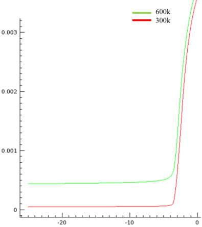
Figure 7: Temperature Characteristics Curves (Linear)
After the temperature increase, the on/off ratio does not show any obvious change, but the device’s threshold voltage Vth shifts from -3.5V to -4V. This indicates that the channel barrier is reduced in a high-temperature environment, making the device easier to turn on. This phenomenon is mainly attributed to the fact that, at high temperatures, the valence band electrons in the semiconductor material acquire higher thermal excitation energy, which leads to an increased carrier concentration in the channel and, consequently, a lower threshold voltage. Moreover, by comparing the transfer curves at the two temperatures on a logarithmic scale (as shown in Figure 8), it is obvious that the saturation current at 600 K is significantly higher than at 300 K at the same gate voltage.
\( {I_{leak}}∝{e^{- \frac{q{Φ_{B}}}{{k_{B}}T}}} \ \ \ (3) \)
From (3), it is evident that at high temperatures, the enhanced thermal excitation of electrons accelerates the generation–recombination rate of carriers in the channel, thereby increasing the device’s saturation current [12]. Meanwhile, the rise in the drain current over the same drain voltage range results in a decrease in the device’s on-state resistance (Ron), which improves the conduction characteristics.
Overall, the simulation results show that the βGa₂O₃ MOSFET exhibits a lower threshold voltage, higher saturation current, and reduced on-state resistance at elevated temperatures, which is significant for the device’s high-temperature stability. However, due to the low thermal conductivity of βGa₂O₃, further optimization of its thermal management is required to enhance the device’s reliability and long-term operational stability.
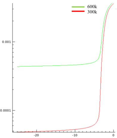
Figure 8: Temperature Characteristics Curves (logarithmic)
5. The Impact of Bulk Defects on MOSFET Devices
5.1. Impact of Bulk Defects on Transfer and Output Characteristics
To study the influence of bulk defects on the electrical characteristics of β‑Ga₂O₃ MOSFET devices, this paper introduces bulk defects with different concentrations into the channel region and compares their effects on the transfer and output curves[13].
As shown in Figure 9, as the concentration of bulk defects increases, the drain current increases significantly, and the threshold voltage (Vth) gradually decreases. At a low defect concentration (Nt= 10¹⁴ cm⁻³), the device exhibits a small off-current, and the threshold voltage remains essentially stable. However, when the defect concentration increases to 10¹⁷ cm⁻³, the drain current increases markedly, and the threshold voltage shifts to more negative values, indicating that the device becomes easier to turn on.
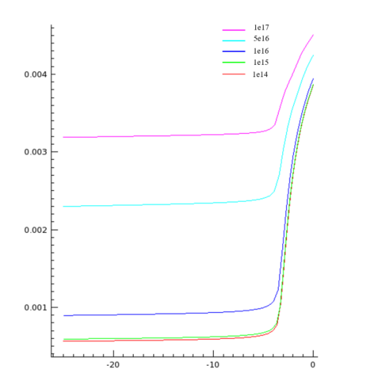
Figure 9: Transfer Curves Considering Bulk Defects
Since bulk defects can supply additional electrons, this leads to an increased carrier concentration in the channel and causes the threshold voltage to drift. This effect can be described using a trap charging model:
\( Δ{V_{th}}=-\frac{q{N_{t}}d}{{ε_{ox}}} \) (4)
Where Nt is the trap state density, d is the oxide thickness, and ε is the dielectric constant of the oxide.
As shown in Figure 10, under the same drain-source voltage Vd, the drain current Id gradually increases with the increasing concentration of bulk defects. This phenomenon can be explained using the SRH recombination model:
\( {R_{SRH}}=\frac{np-n_{i}^{2}}{{τ_{n}}(p+{p_{t}})+{τ_{p}}(n+{n_{t}})}\ \ \ (5) \)
Where n and p denote the electron and hole concentrations, respectively; ni is the intrinsic carrier concentration; τn and τp represent the electron and hole lifetimes, respectively; and nt is the trap state density.
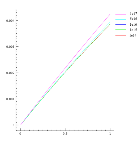
Figure 10: Output Curves Considering Bulk Defects
When the defect density is high, the SRH recombination rate decreases, resulting in an increase in the free carrier concentration, which leads to a significant rise in leakage current. Meanwhile, in the low Vd region, the current still exhibits a linear relationship, indicating that the MOSFET's channel control capability remains effective. However, the overall conduction current increases with the defect concentration, suggesting a decrease in the device’s on-state resistance (Ron).
5.2. Impact of Bulk Defects on Device Off-State Characteristics
With the βGa₂O₃ MOSFET initially set to the off-state, the study investigates how the current density distribution of the leakage current varies with the concentration of bulk defects. As shown in Figure 11, as the defect density gradually increases from 1×1014 cm−3 to 1×1017 cm−3, the device's leakage current correspondingly rises, indicating a transition from the off-state toward the on-state. This phenomenon can be explained in terms of carrier concentration and band modulation [14].
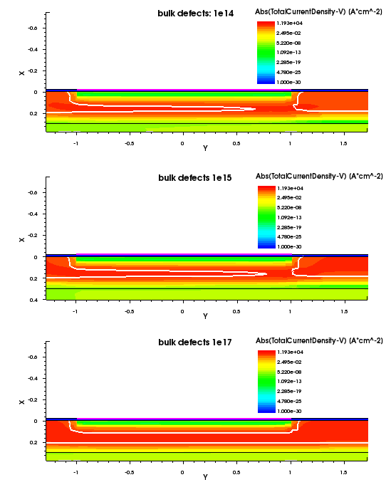
Figure 11: The current density distribution of different bulk defect
At a low defect density of 1×1014 cm−3, the influence of bulk traps is minimal, and the channel can still effectively maintain a high barrier to prevent electrons from passing through; hence, the leakage current remains small and the device stays in the off-state. However, when the defect density increases to 1×1016 cm−3, the device’s leakage current begins to rise noticeably. This is because a high concentration of defects introduces more shallow donor states or additional carrier recombination centers, which increases the intrinsic carrier concentration in the channel region. As a result, the channel barrier is lowered, allowing a small number of electrons to leak through the barrier to the drain, thereby forming a higher leakage current.
When the defect density is further increased to 1×1017 cm−3, the device’s ability to remain off is almost completely lost, exhibiting a clear on-state. At this point, the large number of bulk defects provides extra carriers, significantly boosting the effective electron concentration in the channel and causing a self-doping effect. Consequently, the channel can no longer maintain the high barrier necessary for the off-state, and the device shows strong leakage current characteristics. The simulation images clearly illustrate this trend, with the current density gradually increasing with the defect concentration. Particularly at high defect densities, the current density distribution in the channel region approaches that of a normally on-state device, indicating that the device has lost its ability to turn off.
Overall, bulk defects have a significant impact on the off-state characteristics of βGa₂O₃ MOSFETs. High defect densities cause the device to transition from an off-state to an on-state. Therefore, in practical device design, it is essential to strictly control the quality of material growth and reduce the bulk defect concentration to ensure the reliability and low leakage current performance of MOSFETs under high-voltage off-state conditions.
6. Conclusion
This paper presents a systematic simulation study of the static characteristics, thermal effects, and bulk defect impacts on β-Ga₂O₃ MOSFETs using Sentaurus TCAD software. The results reveal a Vth of −3.5 V and a BV of 100 V, demonstrating promising potential for power applications. However, thermal effects significantly degrade device stability, as evidenced by a pronounced leakage current increase and a negative threshold voltage shift with rising temperature (e.g., 300 K to 600 K). Furthermore, bulk defect concentration exceeding 1×10¹⁷ cm⁻³ induces an anomalous off-to-on state transition, characterized by drain current elevation and threshold voltage reduction, highlighting the critical role of defect engineering. While β-Ga₂O₃ MOSFETs exhibit advantages in ultra-wide bandgap and high critical breakdown electric field for high-power applications, challenges including low thermal conductivity (~27 W/m·K) and defect sensitivity necessitate further optimization. Future efforts should focus on improving crystal growth quality, developing advanced thermal management strategies, and suppressing bulk defects to enhance operational stability and long-term reliability.
References
[1]. Gao Jiacheng. Research on Novel Gallium Oxide Power Devices [D]. University of Electronic Science and Technology of China, 2023.
[2]. Higashiwaki M, Sasaki K, Kuramata A, et al. Gallium oxide (Ga2O3) metal-semiconductor fieldeffect transistors on single-crystal β-Ga2O3 (010) substrates[J]. Applied Physics Letters, 2012,
[3]. Higashiwaki M, Sasaki K, Kamimura T, et al. Depletion-mode Ga2O3 metal-oxidesemiconductor field-effect transistors on β-Ga2O3 (010) substrates and temperature dependence of their device characteristics[J]. Applied Physics Letters, 2013, 103(12): 123511
[4]. Wong M H, Sasaki K, Kuramata A, et al. Field-plated Ga2O3 MOSFETs with a breakdown
[5]. Chabak K D, McCandless J P, Moser N A, et al. Recessed-Gate Enhancement-Mode β-Ga2O3 MOSFETs[J]. IEEE Electron device letters, 2017, 39(1): 67-70.
[6]. Zeng K, Vaidya A, Singisetti U. 1.85 kV breakdown voltage in lateral field-plated Ga2O3 MOSFETs[J]. IEEE Electron Device Letters, 2018, 39(9): 1385-1388.
[7]. Sharma S, Zeng K, Saha S, et al. Field-plated lateral Ga2O3 MOSFETs with polymer passivation and 8.03 kV breakdown voltage[J]. IEEE Electron Device Letters, 2020, 41(6): 836-839.
[8]. Wang Y, Gong H, Jia X, et al. Demonstration of β-Ga2O3 Superjunction-Equivalent MOSFETs[J]. IEEE Transactions on Electron Devices, 2022, 69(4): 2203-2209.
[9]. Peng Xiaosong. Structural Design and Characteristic Research of Gallium Oxide Power Field-Effect Transistors [D]. University of Electronic Science and Technology of China, 2024.
[10]. Qiao Rundi. Research on Vertical Gallium Oxide MOSFET Model and Device Design [D]. Xidian University, 2021
[11]. Wang Guanfei. Research on Enhancement/Depletion Mode β-Ga₂O₃ Field-Effect Transistors [D]. Xidian University, 2021.
[12]. Liu Dinghe. Solutions to Thermal Issues in Ultra-Wide Bandgap Gallium Oxide Devices [J]. Electronics and Packaging, 2024, 24(11):90.
[13]. Wang Lei. Research on Breakdown Characteristics of Gallium Oxide Lateral Field-Effect Transistors [D]. Nanjing University of Posts and Telecommunications, 2023.
[14]. Jiang Zhuolin. Research on Mechanism and Reliability of Novel High-Voltage Low-Power Gallium Oxide MOSFETs [D]. University of Electronic Science and Technology of China, 2024.
Cite this article
Zhou,J. (2025). Research on Simulation Methodology for Gallium Oxide-Based MOSFETs: Electrothermal Characteristics and Reliability Degradation Mechanism. Applied and Computational Engineering,141,60-69.
Data availability
The datasets used and/or analyzed during the current study will be available from the authors upon reasonable request.
Disclaimer/Publisher's Note
The statements, opinions and data contained in all publications are solely those of the individual author(s) and contributor(s) and not of EWA Publishing and/or the editor(s). EWA Publishing and/or the editor(s) disclaim responsibility for any injury to people or property resulting from any ideas, methods, instructions or products referred to in the content.
About volume
Volume title: Proceedings of the 3rd International Conference on Mechatronics and Smart Systems
© 2024 by the author(s). Licensee EWA Publishing, Oxford, UK. This article is an open access article distributed under the terms and
conditions of the Creative Commons Attribution (CC BY) license. Authors who
publish this series agree to the following terms:
1. Authors retain copyright and grant the series right of first publication with the work simultaneously licensed under a Creative Commons
Attribution License that allows others to share the work with an acknowledgment of the work's authorship and initial publication in this
series.
2. Authors are able to enter into separate, additional contractual arrangements for the non-exclusive distribution of the series's published
version of the work (e.g., post it to an institutional repository or publish it in a book), with an acknowledgment of its initial
publication in this series.
3. Authors are permitted and encouraged to post their work online (e.g., in institutional repositories or on their website) prior to and
during the submission process, as it can lead to productive exchanges, as well as earlier and greater citation of published work (See
Open access policy for details).
References
[1]. Gao Jiacheng. Research on Novel Gallium Oxide Power Devices [D]. University of Electronic Science and Technology of China, 2023.
[2]. Higashiwaki M, Sasaki K, Kuramata A, et al. Gallium oxide (Ga2O3) metal-semiconductor fieldeffect transistors on single-crystal β-Ga2O3 (010) substrates[J]. Applied Physics Letters, 2012,
[3]. Higashiwaki M, Sasaki K, Kamimura T, et al. Depletion-mode Ga2O3 metal-oxidesemiconductor field-effect transistors on β-Ga2O3 (010) substrates and temperature dependence of their device characteristics[J]. Applied Physics Letters, 2013, 103(12): 123511
[4]. Wong M H, Sasaki K, Kuramata A, et al. Field-plated Ga2O3 MOSFETs with a breakdown
[5]. Chabak K D, McCandless J P, Moser N A, et al. Recessed-Gate Enhancement-Mode β-Ga2O3 MOSFETs[J]. IEEE Electron device letters, 2017, 39(1): 67-70.
[6]. Zeng K, Vaidya A, Singisetti U. 1.85 kV breakdown voltage in lateral field-plated Ga2O3 MOSFETs[J]. IEEE Electron Device Letters, 2018, 39(9): 1385-1388.
[7]. Sharma S, Zeng K, Saha S, et al. Field-plated lateral Ga2O3 MOSFETs with polymer passivation and 8.03 kV breakdown voltage[J]. IEEE Electron Device Letters, 2020, 41(6): 836-839.
[8]. Wang Y, Gong H, Jia X, et al. Demonstration of β-Ga2O3 Superjunction-Equivalent MOSFETs[J]. IEEE Transactions on Electron Devices, 2022, 69(4): 2203-2209.
[9]. Peng Xiaosong. Structural Design and Characteristic Research of Gallium Oxide Power Field-Effect Transistors [D]. University of Electronic Science and Technology of China, 2024.
[10]. Qiao Rundi. Research on Vertical Gallium Oxide MOSFET Model and Device Design [D]. Xidian University, 2021
[11]. Wang Guanfei. Research on Enhancement/Depletion Mode β-Ga₂O₃ Field-Effect Transistors [D]. Xidian University, 2021.
[12]. Liu Dinghe. Solutions to Thermal Issues in Ultra-Wide Bandgap Gallium Oxide Devices [J]. Electronics and Packaging, 2024, 24(11):90.
[13]. Wang Lei. Research on Breakdown Characteristics of Gallium Oxide Lateral Field-Effect Transistors [D]. Nanjing University of Posts and Telecommunications, 2023.
[14]. Jiang Zhuolin. Research on Mechanism and Reliability of Novel High-Voltage Low-Power Gallium Oxide MOSFETs [D]. University of Electronic Science and Technology of China, 2024.