


1. Introduction
Gallium nitride (GaN) and indium antimonide (InSb) are two important III-V semiconductors with distinct properties and applications. GaN, characterized by its wide bandgap of 3.4 eV, high electron mobility, and thermal conductivity, is well-suited for high-power and high-frequency applications. Its excellent stability and resistance to electromagnetic radiation enable it to operate effectively under extreme conditions, making it a key material for blue LEDs, high-frequency lasers, radar systems, and satellite solar cells [1]. In addition, GaN's high efficiency and low on-resistance enhance its role in integrated circuits, reducing the size and weight of consumer electronics such as smartphones and laptops. Its excellent thermal resistance also addresses the challenge of fast charging lithium-ion batteries, as exemplified by Tesla's Supercharger stations [2]. Conversely, InSb features a narrow bandgap of 0.17 eV at 300 K, making it highly sensitive to infrared light and ideal for applications in infrared detection, such as infrared cameras, missile navigation, and astronomy [3]. InSb-based detectors have high electron mobility and low noise levels, enabling accurate imaging even in low-signal environments, which is critical for military surveillance and fire detection. However, these detectors require regular recalibration and operation at cryogenic temperatures (about 80 K). InSb can be used as a source of terahertz radiation, and its use in high-speed transistor quantum wells further highlights its importance in advanced technologies [3].
In recent years, the electric vehicle (EV) market has been expanding rapidly, growing from a 4% share in 2020 to 18% in 2023 [4], highlighting the urgent need for efficient power conversion technology. Compared with traditional internal combustion engine vehicles, electric vehicles can reduce greenhouse gas emissions by about 80% [3]. In addition, electric vehicles have economic benefits such as reduced maintenance costs and reduced dependence on renewable energy [5]. These are key to the development of electric vehicles. However, one of the main challenges facing the popularization of electric vehicles remains the long charging time [6], and the cumulative charging time of tram systems is significantly longer than that of traditional vehicles [7]. Semiconductor materials play a crucial role in enhancing the power conversion efficiency of electric vehicle chargers. However, traditional silicon-based semiconductors face inherent limitations, prompting researchers to explore wide-bandgap materials such as silicon carbide (SiC) and gallium nitride (GaN) [2]. Among these, GaN has emerged as a highly promising candidate for next-generation power converters due to its low on-resistance, exceptional thermal stability, and ability to withstand high electric fields, enabling faster and more efficient charging solutions.
This study seeks to examine the advantages and challenges associated with the application of Gallium Nitride (GaN) and Indium Antimonide (InSb) in semiconductor power electronics. In parallel with a comprehensive comparison of key semiconductor materials—such as Silicon (Si), Gallium Arsenide (GaAs), Lithium Niobate (LiNbO₃), and Graphene—this research leverages existing datasets and utilizes R software for in-depth statistical analysis and visualization. The study investigates the fundamental properties of GaN and InSb, including refractive index, bandgap, and power conversion performance, while also evaluating their potential integration challenges. By comparing these materials' unique properties in both electronic and optical domains, this research aims to provide valuable insights into the future development of high-efficiency semiconductor materials for electronic and energy applications.
2. Overview of optical communication and photonic chip materials
2.1. Advancements and applications of optical communication
The communication process begins by encoding data into an electrical signal, which is then converted into an optical signal by a laser. The optical signal is modulated through techniques such as amplitude modulation, frequency modulation, and phase modulation, allowing the signal to carry more information [8]. The optical signal is then transmitted through the optical fiber using total internal reflection. Optical signals have very little loss and therefore can be transmitted over longer distances. However, the signal will still attenuate over longer distances, so it needs to be amplified with an optical amplifier. At the receiving end, a photodetector converts the optical signal back into an electrical signal, where a demodulator extracts the original data to complete the communication process.
Compared with traditional electric communication, optical communication has the following advantages. First, the bandwidth of optical communication is wider, enabling the transmission of larger amount of data. Second, the transmission distance is longer because optical communication has low transmission loss. Third, optical signals are resistant to electromagnetic interference, making optical communication particularly suitable for high-noise environments such as industrial and medical settings. Finally, optical communication provides a higher level of security, as optical signals are confined to specific fibers, reducing the risk of interception.
Optical communication is widely used in daily life. Optical fiber communication is the foundation of modern telecommunication networks. Backbone networks, metropolitan area networks, and access networks, etc. mainly rely on optical fiber technology to realize large-scale data transmission. Through optical fiber communication, users can enjoy high-speed broadband Internet access, voice communication and video conferencing. Fiber optic networks can transmit data at rates of hundreds of Gbps or even Tbps, ensuring fast and stable Internet services. In the medical field, fiber optic sensors can be used for real-time monitoring of patients' physiological data, such as temperature, pressure, and blood flow rate. Additionally, the anti-interference and security features of optical communication make it vital in military and aerospace applications, where high-security data transmission is required.
2.2. Photonic chip
A photonic chip is a semiconductor device that utilizes photons for information transmission and processing. The core advantage of this chip is the extremely fast transmission speed of light and low energy consumption. The photonic chip contains several very important devices. First, the waveguide, which is similar to a wire in an electronic circuit, is responsible for transmitting optical signals inside the chip. Second, the optical modulator, which converts electrical signals into optical signals, or modulates the optical signals, changing their intensity, phase or frequency in order to encode information. Third, photodetector, which converts optical signals into electrical signals for subsequent processing or output [9]. Compared to traditional electronic chips, photonic chips have significant advantages. The extremely fast propagation speed of light enables photonic chips to meet the communication needs of low latency and high bandwidth. In addition, since optical signals generate almost no heat during transmission, photonic chips consume less power than electronic chips with resistance heating problems and do not require additional cooling systems. However, the manufacturing and integration of photonic chips are difficult, and mass production still faces great challenges.
At present, photonic chips are widely used in high-speed communication fields such as data centers and Internet infrastructure. Their speed also helps to improve the performance of high-speed computers (HPC) and facilitate large-scale data processing for artificial intelligence and machine learning. In addition, due to their natural anti-interference characteristics and the potential for quantum state superposition and entanglement, photonic chips have great potential in the development of future quantum computers.
2.3. Important materials in photonic chips
The performance of photonic chips depends largely on the choice of materials used in their manufacture, and different materials have their own advantages and disadvantages. Silicon (Si) is widely used in waveguides, modulators, and detectors due to its excellent thermal stability, electrical properties, and compatibility with existing semiconductor technologies, but its large direct bandgap limits the luminous efficiency and requires integration with other materials. Gallium nitride (GaN) is suitable for short-wavelength optical communications and high-frequency photonic chips, and has good resistance to electrical breakdown and high-temperature stability, but the manufacturing process is complex and costly. Gallium arsenide (GaAs) is widely used in photodetectors, LEDs, and laser diodes due to its direct bandgap characteristics, but its integration with silicon-based technology is difficult. Lithium niobate (LiNbO3) has a strong electro-optical effect and is suitable for high-speed optical signal modulation, but its integration with silicon-based processes is challenging.
When selecting materials for optical communications and photonic chips, several key properties must be considered, including optical, electrical, mechanical, and thermal properties. Optical properties such as refractive index and absorption coefficient are critical to light transmission efficiency. Electrical properties, including conductivity and electro-optical effects, determine the suitability of a material for signal modulation and processing. Mechanical properties, including hardness and machinability, affect manufacturing costs and product integration, while thermal properties affect the material's ability to dissipate heat and maintain stability under high power conditions.
3. Methodology
This paper mainly selects four materials, namely silicon (Si), gallium arsenide (GaAs), lithium niobate (LiNbO3) and graphene . First of all, Si is one of the earliest developed semiconductor materials and is widely used in electronic devices and communications. Silicon offers high purity, large-scale production, and cost efficiency, but its indirect bandgap limits its effectiveness in optoelectronic applications like LEDs and laser diodes. However, its compatibility with existing manufacturing processes and ability to form high-quality oxide layers make it indispensable in the semiconductor industry [10]. GaAs is a III-V direct bandgap semiconductor with a wider bandgap and excellent thermal stability compared to silicon. GaAs exhibit high electron mobility and saturated electron velocity, which is suitable for high-frequency applications such as integrated circuits and laser diodes. Despite its high manufacturing cost, GaAs still have advantages in high-performance applications. LiNbO3 is an important material in the field of optical communications, especially for optical modulators. Its electro-optical properties enable it to modulate optical signals without converting the signal, maintaining the high-speed performance of optical networks. Although the production cost is high, its advantages in high-precision and high-efficiency applications make its cost reasonable. The last material is graphene. Graphene is an emerging semiconductor material that has attracted much attention due to its excellent electrical and mechanical properties and high electron mobility. Graphene is ideal for high-speed electronic devices, integrated circuits, and touch screens, but its lack of a natural bandgap restricts its use in digital logic circuits. While production costs have decreased, large-scale applications remain challenging. To directly compare the properties of these materials, this paper employs R to generate histograms that visualize the data effectively. The R packages used for this purpose include tidyr for organizing and analyzing the data and ggplot2 for creating bar charts. The choice of R is driven by its robust capabilities in data handling and visualization, allowing for a comprehensive analysis of the materials' optical properties.
4. Analysis and result
4.1. Analysis process
The analysis for this study begins with the definition of key material properties, including refractive index, bandgap, nonlinear optical coefficients, and the number of major applications. Each property plays a vital role in determining whether a material is suitable for optical communications and semiconductor applications: The refractive index is a critical property in optical communications, particularly in the manufacturing of optical fibers. Optical fibers rely on the difference in refractive indices between core and cladding materials to achieve total internal reflection, thereby guiding light efficiently over long distances. High refractive index materials can enhance this effect, reducing signal loss and improving transmission efficiency.
The bandgap is another fundamental property that influences a material's stability and conductivity. A wider bandgap generally implies better thermal stability and the ability to operate at higher voltages, which is advantageous for high-power applications. Conversely, a narrower bandgap facilitates higher electron mobility, making the material suitable for high-speed electronic devices. The nonlinear optical coefficient is also significant, particularly for applications involving high-intensity light, such as lasers and optical modulators. Materials with high nonlinear coefficients can efficiently convert light frequencies and enable advanced functionalities like wavelength conversion and optical switching.
4.2. Data processing and visualization
Once the data is structured into variables, it is transformed into a CSV format for compatibility with R's plotting methods. The pivot_longer function in R is then used to reshape the data into a long format, which is more suitable for creating comparative plots. The ggplot2 package is employed to generate bar charts, with the horizontal axis representing the materials and the vertical axis showing the values of various properties. The geom_bar method is used to create the bars, with stat=identity ensuring that the height of each bar reflects the actual data values(see Figure 1).
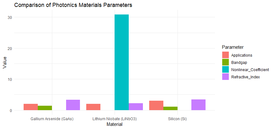
Figure 1: Comparison of photonics materials parameters
The position=dodge parameter arranges the bars side by side for easy comparison. In addition to bar charts, scatter plots are also created using the geom_point method to compare two properties directly(Figure 2). This scatter plot provides a clear visualisation of the relationship between the refractive index and birefringence of different materials, illustrating how these fundamental properties vary across materials. The theme function in ggplot2 is used to customize the appearance of the plots, ensuring that they are both informative and aesthetically pleasing.
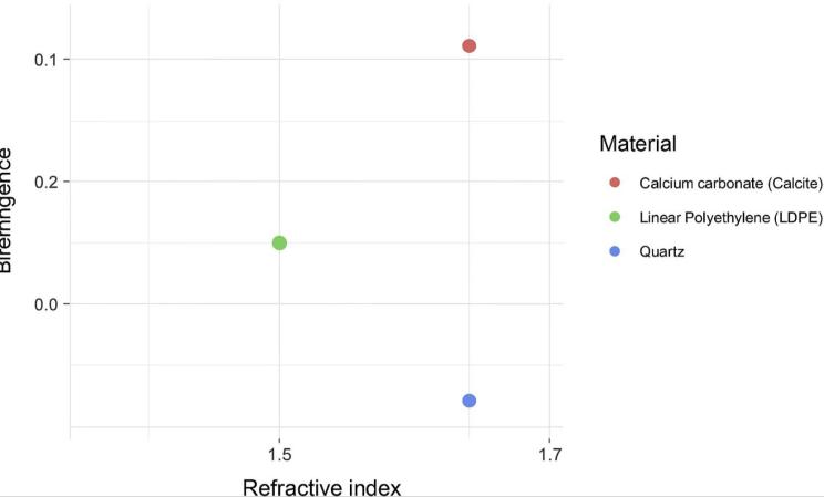
Figure 2: Refractive index vs. birefringence
The final step involves saving the plots using the ggsave function, which allows for high-resolution export in various formats such as PNG, PDF, or SVG. The resulting charts clearly illustrate the comparative advantages of each material, providing valuable insights for selecting the appropriate semiconductor for specific optical communication applications.
4.3. Result
This comparative analysis of semiconductor materials underscores the distinct advantages and trade-offs associated with each material, offering valuable insights into their applications in optical communication and electronic devices. By leveraging R for data visualization, this study provides a clear and effective comparison of key material properties, facilitating an informed selection process. Silicon, gallium arsenide, lithium niobate, and graphene each exhibit unique strengths tailored to different application requirements. The analysis highlights the critical balance between cost, performance, and functionality, emphasizing the need for a strategic approach to material selection. For instance, silicon's low cost and well-established manufacturing processes make it ideal for large-scale applications, whereas gallium arsenide's superior high-frequency performance justifies its higher production cost in specialized fields. Overall, the visual comparison of these materials reinforces the necessity of carefully weighing optical properties against production costs when selecting semiconductors for optical communication technologies.
5. Discussion
The development of photonic chips has brought both important opportunities and challenges. Despite its significant advantages in speed and energy efficiency, complex manufacturing processes, heat dissipation management and material compatibility issues are still key factors limiting its widespread application. For example, although silicon photonics technology is compatible with existing semiconductor manufacturing processes, due to the indirect bandgap characteristics of silicon, other materials often need to be introduced, which increases production complexity and cost uncertainty. In addition, in high-density integrated environments such as data centers, ensuring thermal stability remains a major challenge, and efficient thermal management strategies are urgently needed to prevent performance degradation and improve system reliability.
Beyond their extensive use in traditional applications, photonic chips are being increasingly explored in quantum computing and artificial intelligence. Due to their inherent parallel processing capabilities and resistance to environmental noise, photonic chips hold significant potential for quantum key distribution and quantum gate operations. In the field of artificial intelligence, photonic chips achieve energy-saving neural network computing through optical matrix multiplication, breaking through the power and latency limitations of electronic accelerators. With the continuous advancement of photonic chip technology, their applications in high-performance computing, quantum communications, artificial intelligence and sustainable energy solutions will be further expanded, promoting the future development of information technology.
6. Conclusion
This study provides a comprehensive comparison of the properties of major semiconductor materials—silicon (Si), gallium arsenide (GaAs), lithium niobate (LiNbO₃), and graphene—and their potential applications in optical communications and photonic chip technology. The study highlights the importance of using R software to analyze and visualize the unique properties of these materials, allowing for clear graphical comparisons to assess their suitability for various electronic and optical applications. The results show that while silicon remains a popular choice for large-scale applications due to its cost-effectiveness and compatibility with existing semiconductor technologies, materials such as GaAs, LiNbO₃, and graphene offer significant advantages in specialized applications such as high-frequency communications and optical signal modulation.
While this study provides valuable insights into the properties of the materials and their potential applications, it has certain limitations. The analysis was primarily focused on theoretical material properties, and did not incorporate actual performance data from field applications. Including such data would provide a more comprehensive understanding of how these materials perform under real-world operating conditions, offering a clearer picture of their practical viability and effectiveness. Future research could focus on the practical use of these materials in real-world applications. This would include studying the integration of GaN and InSb in electric vehicle power converters, exploring their long-term performance, and evaluating the scalability of their manufacturing processes. Additionally, further research could delve deeper into the environmental sustainability of these materials, evaluating their lifecycles, energy consumption, and waste management issues.
References
[1]. Amir, H. A. A. A., Fakhri, M. A., & Alwahib, A. A. (2021). Review of GaN optical device characteristics, applications, and optical analysis technology. Materials Today: Proceedings,42, 2815-2821.
[2]. Liu, T. (2021, January). Analysis on the application, development, and future prospects of Gallium Nitride (GaN). In 2020 International Conference on Optoelectronic Materials and Devices(Vol. 11767, pp. 200-205). SPIE.
[3]. Kozlov, R. Y., Kormilitsina, S. S., Molodtsova, E. V., & Zhuravlev, E. O. (2021). Growth of 100 mm indium antimonide single crystals by modified Czochralski technique.Modern Electronic Materials,7(2), 73-78.
[4]. Zhao, W., Zhang, C., Wang, Y., & Li, J. (2019). Lithium-ion battery fast charging: A review. eTransportation, 1, 100011. https://doi.org/10.1016/j.etran.2019.100011
[5]. Durgadevi, M. (2021). Generative Adversarial Network (GAN): A general review on different variants of GAN and applications. In 2021 6th International Conference on Communication and Electronics Systems (ICCES) (pp. 1-8). IEEE.
[6]. Udabe, A., Baraia-Etxaburu, I., & Diez, D. G. (2023). Gallium nitride power devices: A state of the art review. Ieee Access, 11, 48628-48650.
[7]. Patil, G., Pode, G., Diouf, B., & Pode, R. (2024). Sustainable Decarbonization of Road Transport: Policies, Current Status, and Challenges of Electric Vehicles. Sustainability, 16(18), 8058.
[8]. Yücel, M., & Açikgöz, M. (2023). Optical communication infrastructure in new generation mobile networks.Fiber and Integrated Optics, 42(2), 53-92.
[9]. Luo, W., Cao, L., Shi, Y., Wan, L., Zhang, H., Li, S., ... & Liu, A. Q. (2023). Recent progress in quantum photonic chips for quantum communication and internet.Light: Science & Applications, 12(1), 175.
[10]. Adcock, J. C., & Ding, Y. (2022). Quantum prospects for hybrid thin-film lithium niobate on silicon photonics.Frontiers of Optoelectronics,15(1), 7.
Cite this article
Ren,F. (2025). Research on Recent Advances in Semiconductor Materials for Power Electronics. Applied and Computational Engineering,144,150-156.
Data availability
The datasets used and/or analyzed during the current study will be available from the authors upon reasonable request.
Disclaimer/Publisher's Note
The statements, opinions and data contained in all publications are solely those of the individual author(s) and contributor(s) and not of EWA Publishing and/or the editor(s). EWA Publishing and/or the editor(s) disclaim responsibility for any injury to people or property resulting from any ideas, methods, instructions or products referred to in the content.
About volume
Volume title: Proceedings of the 3rd International Conference on Functional Materials and Civil Engineering
© 2024 by the author(s). Licensee EWA Publishing, Oxford, UK. This article is an open access article distributed under the terms and
conditions of the Creative Commons Attribution (CC BY) license. Authors who
publish this series agree to the following terms:
1. Authors retain copyright and grant the series right of first publication with the work simultaneously licensed under a Creative Commons
Attribution License that allows others to share the work with an acknowledgment of the work's authorship and initial publication in this
series.
2. Authors are able to enter into separate, additional contractual arrangements for the non-exclusive distribution of the series's published
version of the work (e.g., post it to an institutional repository or publish it in a book), with an acknowledgment of its initial
publication in this series.
3. Authors are permitted and encouraged to post their work online (e.g., in institutional repositories or on their website) prior to and
during the submission process, as it can lead to productive exchanges, as well as earlier and greater citation of published work (See
Open access policy for details).
References
[1]. Amir, H. A. A. A., Fakhri, M. A., & Alwahib, A. A. (2021). Review of GaN optical device characteristics, applications, and optical analysis technology. Materials Today: Proceedings,42, 2815-2821.
[2]. Liu, T. (2021, January). Analysis on the application, development, and future prospects of Gallium Nitride (GaN). In 2020 International Conference on Optoelectronic Materials and Devices(Vol. 11767, pp. 200-205). SPIE.
[3]. Kozlov, R. Y., Kormilitsina, S. S., Molodtsova, E. V., & Zhuravlev, E. O. (2021). Growth of 100 mm indium antimonide single crystals by modified Czochralski technique.Modern Electronic Materials,7(2), 73-78.
[4]. Zhao, W., Zhang, C., Wang, Y., & Li, J. (2019). Lithium-ion battery fast charging: A review. eTransportation, 1, 100011. https://doi.org/10.1016/j.etran.2019.100011
[5]. Durgadevi, M. (2021). Generative Adversarial Network (GAN): A general review on different variants of GAN and applications. In 2021 6th International Conference on Communication and Electronics Systems (ICCES) (pp. 1-8). IEEE.
[6]. Udabe, A., Baraia-Etxaburu, I., & Diez, D. G. (2023). Gallium nitride power devices: A state of the art review. Ieee Access, 11, 48628-48650.
[7]. Patil, G., Pode, G., Diouf, B., & Pode, R. (2024). Sustainable Decarbonization of Road Transport: Policies, Current Status, and Challenges of Electric Vehicles. Sustainability, 16(18), 8058.
[8]. Yücel, M., & Açikgöz, M. (2023). Optical communication infrastructure in new generation mobile networks.Fiber and Integrated Optics, 42(2), 53-92.
[9]. Luo, W., Cao, L., Shi, Y., Wan, L., Zhang, H., Li, S., ... & Liu, A. Q. (2023). Recent progress in quantum photonic chips for quantum communication and internet.Light: Science & Applications, 12(1), 175.
[10]. Adcock, J. C., & Ding, Y. (2022). Quantum prospects for hybrid thin-film lithium niobate on silicon photonics.Frontiers of Optoelectronics,15(1), 7.