


1. Introduction
With the popularization of portable devices and the Internet of Things (IoT), low power consumption has become a critical objective in circuit design [1-2]. The rapidly growing demand for low power amplifier applications, such as remote sensing and biomedical devices, has pushed amplifier designs to meet stringent specifications, including gain, bandwidth, power consumption, and circuit noise [2-3]. Subthreshold MOSFET transistor amplifiers, which operate at low voltage and low current, can significantly reduce power consumption while maintaining relatively high performance, thereby addressing this demand [1-2]. As semiconductor technology advances, leading to the continuous scaling down of MOSFET dimensions, issues such as leakage current and power consumption in traditional operating modes have become increasingly prominent [4]. In scaling scenarios where power supply and dimensions shrink at the same rate, the subthreshold leakage current and associated static power consumption of transistors increase, resulting in performance degradation [1]. Additionally, at low voltages, the gain and linearity of traditional MOSFET amplifiers decrease. However, in this study, the subthreshold MOSFET amplifiers can effectively solve these issues after three times of optimization simulation design in LT sipice.
The key distinction between subthreshold MOSFET transistor amplifiers and traditional MOSFET amplifiers operating in the saturation region lies in the operating region of the former, which is the subthreshold region [1, 2, 5], where the gate-source voltage is less than the threshold voltage \( {(V_{GS}} \lt {V_{th}}) \) [5]. In this region, the operating current of the transistor is the subthreshold leakage current [1]. For amplifier circuits, a simple configuration can consist of three transistors forming a CMOS inverter-based amplifier [2]. However, such circuits are susceptible to power supply fluctuations, noise, and other factors [6]. In contrast, more complex circuits, such as differential pair circuits with current mirror loads, known as transconductance amplifiers, offer advantages such as higher linearity, gain, and effective suppression of common-mode noise. Operational Transconductance Amplifiers (OTAs), due to their superior performance, are indispensable components in many analog circuits and systems and are widely used in various radio frequency (RF) and intermediate frequency (IF) applications [7-8].
This paper presents a three-stage optimization of an amplifier circuit, ultimately designing a relatively simple CMOS differential operational transconductance amplifier operating in the subthreshold region. It aims to achieve higher gain and lower power consumption. LTspice simulations demonstrate the performance metrics of this differential operational transconductance amplifier, comparing it with the initial design and highlighting its superiority. This paper contributes to the exploration of ultra-low-power amplifier circuit design.
2. Methodology
The final design of the differential operational transconductance amplifier was achieved through continuous optimization of a simple circuit. The MOSFETs in the designed circuit for simulation were fabricated using 180 nm CMOS technology, with a supplied voltage of 1.8 V.
2.1. Amplifier 1
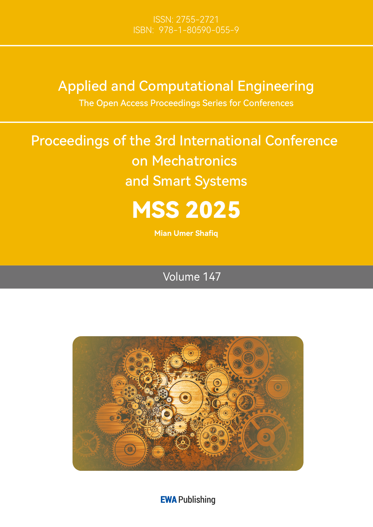
Initially, as shown in Figure 1, three transistors were assembled to form a CMOS inverter-based amplifier. By analyzing the equivalent small-signal circuit of this single-stage amplifier, the voltage gain \( ({A_{V}}) \) of the amplifier can be derived as:
\( {A_{v}}=-({G_{m}}-\frac{1}{{R_{f}}})({R_{o}} ||{ R_{f}}) \) (1)
where \( {G_{m}}={g_{m1}}+{g_{m2}} \) and \( {R_{o}}={r_{o1}} || { r_{o2}} \) . It can be seen that to maximize the voltage gain, the feedback resistor must be very large. However, in general, directly using a very large feedback resistor in integrated circuits is impractical. This issue can be effectively addressed by utilizing a transistor operating in the cutoff region a PMOS transistor was used here, denoted as \( {M_{f}} \) ) as an extremely large resistance in the feedback path [2]. Since the transistor's channel is not conducting in this region, only a minimal leakage current exists, resulting in an equivalent resistance that is extremely high. After the circuit was set up, it was simulated using LTspice, and its performance metrics, such as gain, bandwidth, power consumption and linearity were measured and recorded.
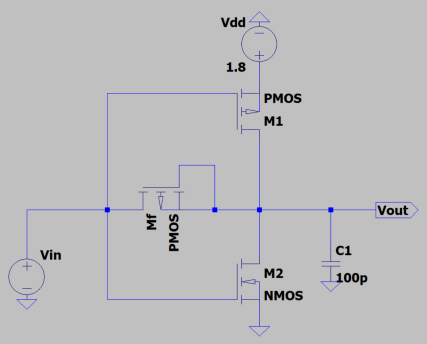
Figure 1: An inverter-based amplifier using a cut-off PMOS for feedback path [7]
2.2. Amplifier 2
Based on it, a transconductance amplifier was constructed, as shown in Figure 2. It consists of an NMOS differential pair circuit ( \( {M_{1}} \) and \( {M_{2}} \) ) and a PMOS current mirror ( \( {M_{3}} \) and \( {M_{4}} \) ). The differential pair circuit could suppress common-mode signals (such as power supply noise and environmental interference) because common-mode signals are identical at both inputs and thus cancel each other out. This characteristic enhances the amplifier's immunity to interference. The current mirror, by replicating the reference current, provides matched currents for the differential pair MOSFETs and the load, thereby improving the circuit's gain and common-mode rejection ratio (CMRR) while maintaining low power consumption. In addition, to ensure the circuit operates stably in the linear region as much as possible, an NMOS ( \( {M_{b}} \) ) was employed as a constant current source to limit the total current of the entire circuit. Although the currents in the two branches of the differential pair are determined by the input differential signal, the total current is always constrained by the tail current source. Consequently, regardless of the input signal swing, the combined current of \( {M_{3}} \) and \( {M_{4}} \) will never exceed the current set by \( {M_{b}} \) . Excessive current would increase power consumption and could potentially exceed the limitations of the fabrication process or thermal dissipation capabilities. By controlling the total current within an appropriate range, a balance between performance and power consumption can be achieved.
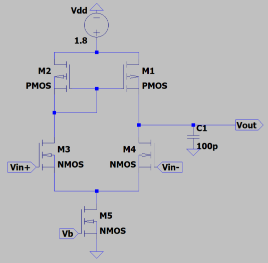
Figure 2: An NMOS differential pair biased with a PMOS current mirror [9]
2.3. Amplifier 3
Subsequently, to further improve the amplifier's gain and bandwidth, an externally biased cascode topology was employed. This topology was represented by two branches, each containing an NMOS ( \( {M_{7}}, {M_{8}} \) ) and a PMOS ( \( {M_{5}}, {M_{6}} \) ), as shown in Figure 3 [8]. This circuit is also known as the wide output range transconductance amplifier. In this cascode design, the input differential pair and the output were implemented through two independent current branches. The output current was generated by mirroring the input current using a cascoded configuration. This design offers higher gain, bandwidth, and output swing. However, it also results in relatively higher power consumption.
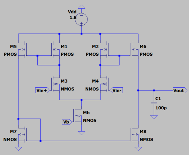
Figure 3: The wide output range transconductance amplifier
2.4. Final Designed Amplifier
As shown in Figure 4, further optimization of the circuit using a two-stage cascode topology was implemented to once again increase the circuit's gain. This design also effectively reduces noise at the input stage [10]. The labels \( {V_{b1}}-{V_{b5}} \) represent the bias voltages to be applied to the corresponding nodes. These voltages are generated by separate bias generation circuits utilizing MOSFETs. The two-stage cascode topology, through its cascaded structure, not only further amplifies the signal but also significantly enhances bandwidth, linearity, and stability, making it suitable for high-performance applications.
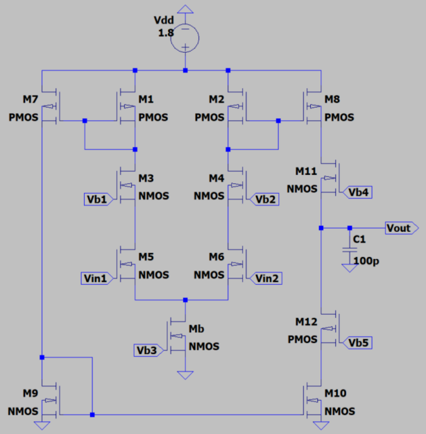
Figure 4: The designed operational transconductance amplifier (OTA) circuit
Each circuit was simulated using LTspice to observe and compare the performance metrics of these amplifier circuits, including gain, bandwidth, power consumption, and linearity.
3. Simulation Results
The simulation results of the above four amplifier circuits are presented in Table 1.
Table 1: Simulation results of the four amplifier circuits
Gain (dB) | Bandwidth (kHz) | Power consumption | Linearity (dBm) | |
Amplifier 1 | 16.5 | 35 | 2.7 μW | 19 |
Amplifier 2 | 29.1 | 87 | 1.9 μW | 15 |
Amplifier 3 | 42.5 | 376 | 1.0 μW | 9 |
Final amplifier | 58.3 | 465 | 1.1 μW | 10 |
It can be seen that the final designed MOSFET amplifier presents superior performance across various aspects, demonstrating good amplification functionality even under the constraint of low power consumption. The amplifier 4 has the highest gain with about 58.3 dB and a wide output range with 465 kHz. The frequency response of the output voltage is shown in the figure 5.
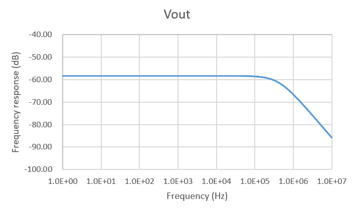
Figure 5: The frequency response of the output voltage
By utilizing NMOS as a constant current source, employing current mirrors, and adopting cascode topology, the performance of the amplifier circuit can be continuously optimized. Ultimately, the proposed circuit consumes only about 1μW of DC power when operating at a supply voltage of 1.8V. However, the bandwidth of this circuit remains relatively narrow (less than 1MHz), making it suitable only for applications involving lower frequency signals. In future work, it is expected that the bandwidth could be increased to at least a few megahertz.
4. Discussion
The results indicate that the designed MOSFET amplifier operating in the subthreshold region can significantly reduce power consumption while maintaining good gain and linearity. The primary reason for this is the circuit's high and nearly constant transconductance. Transconductance \( {g_{m}} \) represents the control capability of the gate-source voltage VGSVGS over the drain current, which can be expressed by Equation (2):
\( {g_{m}}=\frac{∂{I_{D}}}{∂{V_{GS}}}=\frac{{I_{D}}}{n{V_{T}}} \) (2)
where n is the subthreshold slope factor. In the subthreshold region, the ratio of transconductance to drain current ( \( \frac{{g_{m}}}{{I_{D}})} \) is high, enabling the MOSFET to deliver substantial transconductance even at low currents, which supports high gain. Additionally, since the drain current is very small, its dependence on the drain-source voltage \( {V_{DS}} \) is weak, resulting in a higher output impedance \( {r_{o}} \) of the MOSFET, which also contributes to the amplifier's gain. Furthermore, the circuit typically operates in small-signal mode with small input signal amplitudes. Therefore, the transconductance \( {g_{m}} \) is almost constant, ensuring good linearity. Moreover, the small current minimizes the impact of device nonlinearities (such as channel length modulation and body effect) on the circuit, leading to lower distortion.
The circuit's bandwidth is generally related to the transconductance \( {g_{m}} \) and the load capacitance \( {C_{L}} ({f_{3dB}}∝\frac{{g_{m}}}{{C_{L}}}) \) . While reducing capacitance can enhance bandwidth, this may compromise gain and linearity. In this study, current reuse techniques were employed to optimize the balance between bandwidth and other circuit performance metrics. Common implementations of current reuse techniques include differential pair current reuse, cascode structures, and multi-stage amplifier current reuse. The first optimization utilized differential pair current reuse, where multiple differential pairs share a tail current source, thereby reducing the total current and power consumption. The differential structure itself also offers good linearity. The second and third optimizations employed the cascode structure. The cascode structure stacks two transistors, sharing the same bias current, achieving high gain and high bandwidth at low power consumption. The lower transistor (common-source stage) provides transconductance, while the upper transistor (common-gate stage) offers high output impedance. The low input capacitance of the common-gate stage reduces the Miller effect, thereby also increasing bandwidth.
5. Conclusion
In this study, an operational transconductance amplifier (OTA) operating in the subthreshold region was designed after several iterations of circuit optimization. Given the increasing demand for low-power amplifiers, this study aims to explore ways to enhance the performance of the amplifier as much as possible while maintaining low power consumption. Thus, it could be more suitable for applications such as medical devices and portable products.
The simulation results, conducted using LTspice, revealed that the final amplifier circuit achieved a gain of 58.3 dB, a bandwidth of 465 kHz, and a power consumption of only 1.1 μW at a supply voltage of 1.8 V. These results highlight the effectiveness of employing techniques such as NMOS constant current sources, current mirrors, and cascode topologies in optimizing amplifier performance. However, the bandwidth remains relatively narrow, limiting the circuit's applicability to low-frequency signal processing. Future work could focus on further increasing the bandwidth to extend the circuit's usability to higher-frequency applications.
However, there are still some limitations. For instance, the simulation did not investigate the impact of temperature on MOSFETs operating in the subthreshold region. Future work could explore the temperature characteristics of MOSFET devices, specifically examining the effects of temperature on threshold voltage and current.
Looking ahead, further optimization of subthreshold MOSFET amplifiers can be achieved through device structure enhancements (three-dimensional architectures such as FinFETs and nanowires) or novel materials (two-dimensional materials and high-mobility channel materials), which improve the subthreshold transconductance and, consequently, gain and bandwidth. The future of subthreshold MOSFET amplifiers will deeply integrate material innovations, circuit architecture optimization, and system-level energy efficiency management, positioning them as core components in ultra-low-power electronic systems.
References
[1]. Sharroush, S. M., Abdalla, Y. S., Dessouki, A. A., & El-Badawy, E.-S. A. (2009). Subthreshold MOSFET transistor amplifier operation. In 2009 4th International Design and Test Workshop (IDT) (pp. 1-6). Riyadh, Saudi Arabia.
[2]. Schmucker, L., Zarkesh-Ha, P., Emmert, L., Rudolph, W., & Gruzdev, V. (2023). A subthreshold CMOS inverter-based amplifier for low power and low noise applications. In 2023 30th IEEE International Conference on Electronics, Circuits and Systems (ICECS) (pp. 1-4). Istanbul, Turkiye.
[3]. Tai, C.-F., Lai, J.-L., & Chen, R.-J. (2006). Using bulk-driven technology to operate in the subthreshold region for designing a low voltage and low current operational amplifier. In 2006 IEEE International Symposium on Consumer Electronics (pp. 1-5). St. Petersburg, Russia.
[4]. Martin-Martinez, J., Rodriguez, R., Nafria, M., & Aymerich, X. (2009). Time-dependent variability related to BTI effects in MOSFETs: Impact on CMOS differential amplifiers. IEEE Transactions on Device and Materials Reliability, 9(2), 305-310.
[5]. Iida, T., Asai, T., Sano, E., & Amemiya, Y. (2009). Offset cancellation with subthreshold-operated feedback circuit for fully differential amplifiers. In 2009 16th IEEE International Conference on Electronics, Circuits and Systems (ICECS) (pp. 140-143). Yasmine Hammamet, Tunisia.
[6]. Manolov, E. D. (2018). Design of CMOS analog circuits in the subthreshold region of operation. In 2018 IEEE XXVII International Scientific Conference Electronics - ET (pp. 1-4). Sozopol, Bulgaria.
[7]. Rezaei, F., & Azhari, S. J. (2010). A highly linear operational transconductance amplifier (OTA) with high common mode rejection ratio. In 2010 International Conference on Signal Acquisition and Processing (pp. 18-22). Bangalore, India.
[8]. Nayak, A., Bonthala, S., Uppoor, Y., & Bhat, M. S. (2019). Design of high gain operational transconductance amplifiers in 180 nm CMOS technology. In 2019 IEEE International Conference on Distributed Computing, VLSI, Electrical Circuits and Robotics (DISCOVER) (pp. 1-4). Manipal, India.
[9]. Chanapromma, C., & Daoden, K. (2010). A CMOS fully differential operational transconductance amplifier operating in the sub-threshold region and its application. In 2010 2nd International Conference on Signal Processing Systems (pp. V2-73-V2-77). Dalian, China. doi: 10.1109/ICSPS.2010.5555220.
[10]. Chaya, N., Ghosh, A., Srinivas, B., & Jain, A. (2020). An ultra-low power low noise operational transconductance amplifier for biomedical front-end applications. In 2020 International Conference on Inventive Computation Technologies (ICICT) (pp. 1020-1023). Coimbatore, India.
Cite this article
Luo,X. (2025). Design of High Performance MOSFET Amplifier in Subthreshold Region. Applied and Computational Engineering,147,127-133.
Data availability
The datasets used and/or analyzed during the current study will be available from the authors upon reasonable request.
Disclaimer/Publisher's Note
The statements, opinions and data contained in all publications are solely those of the individual author(s) and contributor(s) and not of EWA Publishing and/or the editor(s). EWA Publishing and/or the editor(s) disclaim responsibility for any injury to people or property resulting from any ideas, methods, instructions or products referred to in the content.
About volume
Volume title: Proceedings of the 3rd International Conference on Mechatronics and Smart Systems
© 2024 by the author(s). Licensee EWA Publishing, Oxford, UK. This article is an open access article distributed under the terms and
conditions of the Creative Commons Attribution (CC BY) license. Authors who
publish this series agree to the following terms:
1. Authors retain copyright and grant the series right of first publication with the work simultaneously licensed under a Creative Commons
Attribution License that allows others to share the work with an acknowledgment of the work's authorship and initial publication in this
series.
2. Authors are able to enter into separate, additional contractual arrangements for the non-exclusive distribution of the series's published
version of the work (e.g., post it to an institutional repository or publish it in a book), with an acknowledgment of its initial
publication in this series.
3. Authors are permitted and encouraged to post their work online (e.g., in institutional repositories or on their website) prior to and
during the submission process, as it can lead to productive exchanges, as well as earlier and greater citation of published work (See
Open access policy for details).
References
[1]. Sharroush, S. M., Abdalla, Y. S., Dessouki, A. A., & El-Badawy, E.-S. A. (2009). Subthreshold MOSFET transistor amplifier operation. In 2009 4th International Design and Test Workshop (IDT) (pp. 1-6). Riyadh, Saudi Arabia.
[2]. Schmucker, L., Zarkesh-Ha, P., Emmert, L., Rudolph, W., & Gruzdev, V. (2023). A subthreshold CMOS inverter-based amplifier for low power and low noise applications. In 2023 30th IEEE International Conference on Electronics, Circuits and Systems (ICECS) (pp. 1-4). Istanbul, Turkiye.
[3]. Tai, C.-F., Lai, J.-L., & Chen, R.-J. (2006). Using bulk-driven technology to operate in the subthreshold region for designing a low voltage and low current operational amplifier. In 2006 IEEE International Symposium on Consumer Electronics (pp. 1-5). St. Petersburg, Russia.
[4]. Martin-Martinez, J., Rodriguez, R., Nafria, M., & Aymerich, X. (2009). Time-dependent variability related to BTI effects in MOSFETs: Impact on CMOS differential amplifiers. IEEE Transactions on Device and Materials Reliability, 9(2), 305-310.
[5]. Iida, T., Asai, T., Sano, E., & Amemiya, Y. (2009). Offset cancellation with subthreshold-operated feedback circuit for fully differential amplifiers. In 2009 16th IEEE International Conference on Electronics, Circuits and Systems (ICECS) (pp. 140-143). Yasmine Hammamet, Tunisia.
[6]. Manolov, E. D. (2018). Design of CMOS analog circuits in the subthreshold region of operation. In 2018 IEEE XXVII International Scientific Conference Electronics - ET (pp. 1-4). Sozopol, Bulgaria.
[7]. Rezaei, F., & Azhari, S. J. (2010). A highly linear operational transconductance amplifier (OTA) with high common mode rejection ratio. In 2010 International Conference on Signal Acquisition and Processing (pp. 18-22). Bangalore, India.
[8]. Nayak, A., Bonthala, S., Uppoor, Y., & Bhat, M. S. (2019). Design of high gain operational transconductance amplifiers in 180 nm CMOS technology. In 2019 IEEE International Conference on Distributed Computing, VLSI, Electrical Circuits and Robotics (DISCOVER) (pp. 1-4). Manipal, India.
[9]. Chanapromma, C., & Daoden, K. (2010). A CMOS fully differential operational transconductance amplifier operating in the sub-threshold region and its application. In 2010 2nd International Conference on Signal Processing Systems (pp. V2-73-V2-77). Dalian, China. doi: 10.1109/ICSPS.2010.5555220.
[10]. Chaya, N., Ghosh, A., Srinivas, B., & Jain, A. (2020). An ultra-low power low noise operational transconductance amplifier for biomedical front-end applications. In 2020 International Conference on Inventive Computation Technologies (ICICT) (pp. 1020-1023). Coimbatore, India.