


1. Introduction
With the rapid development of IT industry, artificial intelligence, 5G communications, intelligent driving and other technologies have emerged, and this has also led to more demand for chip performance. Semiconductor materials from the beginning of the silicon, germanium as the representative of the elemental semiconductor, the development of gallium arsenide (GaAs), indium phosphide (InP) as the representative of the compound semiconductor, and then to the current large-scale use of gallium nitride (GaN), silicon carbide (SiC) as the representative of the wide-bandwidth semiconductor materials.
Nowadays, however, it is more and more difficult to downsize the chip due to the short channel effect, parasitic capacitance, heat dissipation problems and other factors. Against this background, diamond material, as an emerging semiconductor material, is gradually attracting the attention of researchers. Diamond has excellent properties such as ultra-high forbidden bandwidth (about 5.5 eV), high carrier mobility and high carrier saturation drift rate, which make it show great potential in high-power, high-frequency and high-temperature electronic devices.
This paper introduces the physical properties of diamond semiconductors, gives an overview of the latest preparation methods and doping methods and analyzes the bottlenecks encountered in industrialization. This paper hopes to provide inspiration for related research workers and promote the further development and application of diamond semiconductor technology.
2. Physical Properties of Diamond
Commonly used as a diamond semiconductor, the crystal structure of octahedral diamond is known to naturally exist as the hardest substance. Diamond has excellent wear resistance. In industrial applications, it can greatly extend the service life of tools. It also has the highest forbidden band width in semiconductor materials, about 5.45ev, can withstand higher voltages without breakdown and reduces thermal noise and leakage current. The high degree of uniformity in the arrangement of diamond atoms also makes diamond far superior to other substances in terms of thermal conductivity. Diamond has an electron mobility of 4500cm²/(V・s), a hole mobility of 3800cm²/(V・s), an excellent carrier mobility, and a low dielectric constant of 5.7, which gives it good electronic properties. As a result, diamond semiconductors show outstanding potential for development among a host of next-generation semiconductors. Table 1 shows a comparison of the parameters of diamond and other wide-band semiconductor materials, and it can be seen that diamond is undoubtedly the most promising wide-band semiconductor material for the future.
Table 1: Comparison of major broadband material parameters [1]
Makings | Diamonds | GaN | Si | GaAs | SiC |
Bandwidth (ev) | 5.45 | 3.45 | 1.12 | 1.43 | 3.2 |
relative permittivity | 5.5 | 8.9 | 11.8 | 12.8 | 9.7 |
Breakdown electric field (MV/cm) | 10 | 3 | 0.3 | 0.4 | 3 |
Electron saturation velocity (x10⁷ cm/s) | 2.7 | 2.5 | 1 | 1 | 2 |
Electron mobility (cm²V-¹s-¹) | 4500 | 900 | 1500 | 6000 | 700 |
Hole mobility (cm²V-¹s-¹) | 3800 | 10 | 600 | 400 | 90 |
Thermal conductivity (Wcm-¹K-¹) | 20 | 1.3~2.1 | 1.5 | 0.5 | 3.7~4.5 |
3. Preparation of Diamond Semiconductors
3.1. Artificial Diamond Synthesis
At present, the mainstream synthesis of artificial diamond is chemical vapor deposition(CVD) method and high pressure and high temperature(HPHT) method.
High Pressure High Temperature (HPHT) is a physical transformation method that catalyzes the precipitation of diamond from a carbon source by means of a high temperature and high pressure, metal catalyst. HPHT method can prepare artificial diamond efficiently and in large quantities, but due to its products of different sizes and more internal defects, it is not suitable for the cutting and preparation of semiconductor materials, so to put into the production of semiconductor diamond materials need to further improve the preparation process and catalyst medium, so as to make the products morphology more stable and less impurity defects.
Chemical vapor deposition (CVD) is a chemical deposition method that deposits a large area of diamond film on a substrate or relies on diamond single crystal seeds to further grow into large single crystals [2]. The most maturely developed method with the highest synthesis efficiency is the microwave plasma chemical vapor deposition (MPCVD), which is based on the principle that a mixture of gases reacts under the action of microwaves to form diamond structural units and deposit them into a film. The artificial diamond synthesized has good purity as well as low impurity defects. However, the edge effect associated with growing seed crystals limits the size of diamond crystals produced by the MPCVD method, resulting in high production costs and challenges for large-scale industrialization.
Currently, the growth of larger-sized single crystals can be realized by heterogeneous substrate epitaxy. However, the lattice constant mismatch and thermal mismatch between substrate and diamond make the dislocation density of the grown diamond usually as high as \( 106~108 cm-2 \) [3]. Solutions to these issues are still under research. Jixiang Jing's team proposed the edge-exposed exfoliation method [4]. 3m tape was used to peel the diamond film grown by MPCVD on silicon substrate, and a 2-inch diamond film was successfully obtained. After comprehensive characterization, the Raman peaks, obtained crystal structure, optical, electrical and thermal properties were comparable to those of the standard single-crystal diamond, with a uniform surface resistance and a good photo-detection performance. In addition, his team can build a reliable device with high peeling performance by calculating the peeling angle and thickness, which provides the feasibility for the edge peeling method to be put into industrialization.
3.2. Doping of Artificial Diamonds
In order to realize the fabrication of semiconductor devices, the doping technique of diamond with non-metallic elements plays a crucial role in changing the electrical properties of diamond. The realization of p-type and n-type conductivity is a fundamental requirement for the preparation, thus becoming the focus of researchers' attention [5].
3.2.1. P-type Doping
Boron doped p-type diamond semiconductor is currently the most mature technology development research direction, primarily due to boron's small atomic radius and high solubility in diamond, which facilitates its replacement of carbon atoms to form vacancies.. There are also many methods for its preparation. For example, boron can be added to synthesized with catalysts under high temperature and high pressure conditions. It also can be used to grow boron-containing diamond single crystals by the method of vapor deposition. Additionally, it can be infiltration at high temperature and high pressure for ordinary artificial diamond or ion implantation [6]. At present, the main problem comes from the defects brought about by diamond growth [7]. Diamond single crystals vegetated by using domestic MPCVD equipment have a variety of defects, such as line dislocations, stacking dislocations, vacancies, twins and so on , and their densities are greater than 104cm-2. These defects may reduces the carrier mobility of diamond semiconductors and limits their application in electronic devices.
3.2.2. N-type Doping
Compared to p-type diamond semiconductors, the development of n-type diamond semiconductors is in a relatively stagnant stage, which is currently one of the biggest technical barriers to the preparation of diamond semiconductor electronic devices.
As one of the common impurities in diamond, nitrogen-donor atoms can significantly affect the optical properties of diamond. Vacancies introduced by nitrogen atoms in diamond crystals form defect centers, which cause diamond to exhibit different colors [8]. These color centers significantly affect the optical properties of diamond semiconductors and improve their luminescence efficiency, which provides for the preparation of semiconductor devices of optical class.
Elemental phosphorus is also one of the choices for n-type doping of diamond, and its doping into diamond is prone to the formation of lattice expansion and distortion, resulting in unstable crystal electrical properties. However, Guo Rui'ang et al. found that it is possible to try to prepare n-type phosphorus doped diamond by high-pressure thermal diffusion method [9]. SIMS detection indicates that phosphorus impurities exhibit the highest surface concentration, with a maximum doping depth of approximately 700 nm. Variable temperature Hall effect tests reveal that electron concentration varies with temperature, an activation energy of 102 meV, a compensation ratio of 0.34, and a low resistivity of 2 Ω·cm at room temperature. It can be seen that the high-pressure thermal diffusion method plays a considerable role in promoting phosphorus doping.
In addition to the above doping of single elements with catalysts, the research and application of "codoping", in which multiple doping elements act together, is also very extensive. Based on the fact that boron can more easily enter into the carbon atom structure, adjusting the ratio of boron-sulfur, boron-nitrogen, and other codoping combinations can increase the doping efficiency of other elements in diamond.
3.3. Devices
The unique properties of diamond semiconductors enable them to be involved in the preparation of many new types of semiconductors.
3.3.1. Power Semiconductor Devices
In terms of power type semiconductor devices, diamond material research has focused on the development of diodes and MOS tubes. Taking diodes as an example, single-crystal diamond pin tubes were prepared by heterogeneous epitaxy, which exhibited good rectification characteristics [10]. Additionally, Schottky diode has a low forward voltage drop, short recovery time, and possesses the ability of fast switching in response to high-frequency signals. Qiliang Wang, et al. designed a Schottky diode structure that substitutes the N-type semiconductor with a field-plate structure, addressing the immaturity of N-type diamond semiconductor doping technology, as illustrated in Fig. 1 [11].. The field plate technique can alleviate the electric field concentration effect at the edges of the Schottky electrodes, enhance the breakdown voltage and reduce the leakage current. However, there is no intrinsic dielectric layer in the diamond, and the high density of interfacial state defects and the fixed charge of the dielectric layer can lead to device reliability problems.
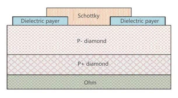
Figure 1: Schematic diagram of Schottky diode structure [11]
In the MOS tube, silicon field-effect tube is widely used in electronic devices. If the diamond material can be used to replace the silicon-based material, its electronic properties will be greatly improved. Taking the popular hydrogen-terminated diamond MOS tube as an example, its principle is to change the surface properties of diamond through hydrogen-terminated modification, so that it shows P-type conductivity at room temperature. According to Shaw-Hua Zhu, et al., the introduction of hydrogen termination can be realized through a remote plasma CVD chamber, followed by isolation, ALD deposition of gate oxides and other steps to complete the preparation of hydrogen-terminated diamond [12].
3.3.2. Sensors and Light Emitting Devices
In terms of sensors and light-emitting devices, the ultra-wide forbidden band of diamond enables it to detect electromagnetic waves with photon energies greater than 5.5ev. Figure 2 shows the structure of an Au-electrode silicon-based diamond detector, which has a low operating dark current, a high light-to-dark current ratio, and a high sensitivity with good photoelectric conversion capability [13].
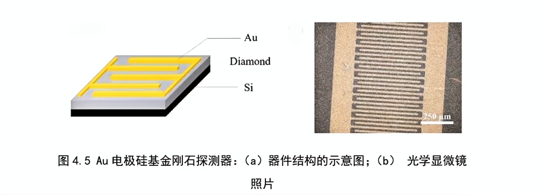
Figure 2: Schematic structure of Au-electrode Si-based diamond detector/optical microscope photo [13]
The research of light-emitting devices prepared based on doped color centers is not yet in the initial stage, and no mature industrialized products have appeared yet. However, theoretically speaking, due to the existence of ultra-high forbidden band, diamond semiconductor can theoretically emit a maximum of about 225nm of light, which can greatly broaden the light-emitting device light-emitting range.
4. Challenges and Prospects
In summary, although diamond semiconductor materials have many advantages, their distance from real industrialization is still facing heavy obstacles.
First of all, the current diamond growth rate is slow and it is difficult to prepare large-size single-crystal diamond materials to meet production. In addition, there is a lack of mature stripping technology, which makes the production cost very high and difficult to put into commercial production. Secondly, the N-doped diamond semiconductor materials currently prepared have low carrier concentration and mobility and high defect density. It is necessary to improve the doping technology to increase the concentration of N-doped ions and doping quality. In addition, in the large-scale production process, semiconductor device design improvement and other aspects also need further research. It can be seen that diamond semiconductors are still a long way from industrialization; there are still many problems that need to be solved.
For future research directions, the improvement of heterogeneous epitaxy, the development of new substrate materials or the existing substrate surface treatment, growth parameter optimization, etc. can help to prepare larger size diamond single crystals; optimization of the CVD process, improve the growth rate of single crystals is conducive to reducing the cost of production, increase production efficiency; looking for a new doping technology, increase the doping concentration can improve the electrical characteristics of N-type semiconductors; explore excessive metal elements and their compounds as new doping elements can also expand the application scope of diamond semiconductors.
5. Conclusion
This paper discusses in detail the physical properties, preparation methods and doping techniques of diamond, and analyzes its current applications in power electronics, optoelectronics and other fields. The research results of major laboratories are sufficient to prove that diamond semiconductor devices have far superior performance than other existing semiconductor devices.Despite challenges in the production process hindering industrialization, improvements in heterogeneous epitaxy enable the preparation of larger diamond single crystals. Enhanced doping technologies, such as ion implantation, will further boost the electrical characteristics of diamond semiconductors. Research on doped color centers will also expedite the deployment of diamond semiconductor devices. Moreover, ongoing optimization of semiconductor device structures will position diamond semiconductors to excel in areas such as power devices, detectors, optical light-emitting devices, and sensors.
However, while this paper explores the potential of diamond semiconductors, it does not deeply analyze their economics and feasibility in practical applications. Looking ahead, diamond semiconductors are expected to lead the semiconductor industry in the future, promote the innovation of electronic devices, and change people's lifestyles. Through continuous research and technological breakthroughs, diamond semiconductors will surely be commercialized in a wider range of fields and show great market potential.
References
[1]. Xuhui Gao. The State-of-the-Art of Diamond Material for Semiconductors, Scientific Consult, 2024, 831(9), 240-243.
[2]. Zhang Wangxi. Research Progress in Synthesis of Diamond Prepared with Chemical Vapour Deposition (CVD), Journal of Ceramics, 2021, 42(4), 538-546
[3]. Mou Caoyuan, Li Genzhuang, Xie Wenliang, Wang Qiliang, Lv Xianyi, Li Liumang, Zou Guangtian. Research Progress in Preparation of Large Size Single Crystal Diamond by Microwave Plasma Chemical Vapor Deposition, ELECTRONICS & PACKAGING, 2023, 23(1), 010104-1-010104-9.
[4]. Jixiang Jing, Fuqiang Sun et al. Scalable production of ultraflat and ultraflexible diamond membrane, Nature, 2024, 636: 627-633.
[5]. ZHANG Xuan, CUI Boyao, MA Yongjian, TANG Wenbo, WEI Zhipeng, ZHANG Baoshun. p-Type and n-Type Doping of Single Crystal Diamond NIU Keyan1, JOURNAL OF SYNTHETIC CRYSTALS, 2022, 51(5): 842-851.
[6]. Na Zhang. Study on micro-quality and semiconductor performance of boron-doped diamond single crystals, 2010.
[7]. Jingsheng Wang. Study on synthesis and Properties of Boron-doped Single Crystals and Polycrystalline Diamond, 2021.
[8]. Wu Tanyang, Xu Sankui, Li Yantao, et al. Research of Doping Diamond with Non-metallic Elements by High Temperature and High Pressure, Guangdong Chemical Industry, 2024, 51(8): 38-40.
[9]. Ruiang Guo, Shuaiqi Li, Jiawei Zhang, Yi Tian, Weiguo Dong and Duanwei He. Phosphorus-doped n-type diamond with high ionization efficiency through high-pressure thermal diffusion, SCIENCE CHINA Materials, 2025, 1-7.
[10]. Genqiang Chen, Xixiang Zhao, Zhongcheng Yu, Zheng Li, Qiang Wei, Fang Lin. Hongxing Wang,Research Progress of Heteroepitaxial Single-Crystal Diamond and Related Electronic Devices, JOURNAL OF SYNTHETIC CRYSTALS, 2023, 52(6):932-944.
[11]. Qiliang Wang, Yiming Zhang, Genjang Li, Li Liumang Li, Shaoheng Cheng, Xianyi Lu, Hongdong Li, Guangtian Zou. Research Progress and Challenges of Diamond Semiconductor and Power Schottky Barrier Diodes, Vacuum Electronics, 2024, 18-28.
[12]. Shaw-Hua Zhu. Investigation of CVD Diamond Preparation and Diamond Metal-Oxide-Semiconductor Field-Effect Transistors, 2022.
[13]. Zengzhong Wang. Study of Hetero-epitaxial Silicon-based Diamond Grown by MPCVD and the MSM Structure Diamond-based Solar Blind UV Detectors, 2024.
Cite this article
Sun,Y. (2025). Overview of Diamond Semiconductor Development and Research Directions. Applied and Computational Engineering,147,121-126.
Data availability
The datasets used and/or analyzed during the current study will be available from the authors upon reasonable request.
Disclaimer/Publisher's Note
The statements, opinions and data contained in all publications are solely those of the individual author(s) and contributor(s) and not of EWA Publishing and/or the editor(s). EWA Publishing and/or the editor(s) disclaim responsibility for any injury to people or property resulting from any ideas, methods, instructions or products referred to in the content.
About volume
Volume title: Proceedings of the 3rd International Conference on Mechatronics and Smart Systems
© 2024 by the author(s). Licensee EWA Publishing, Oxford, UK. This article is an open access article distributed under the terms and
conditions of the Creative Commons Attribution (CC BY) license. Authors who
publish this series agree to the following terms:
1. Authors retain copyright and grant the series right of first publication with the work simultaneously licensed under a Creative Commons
Attribution License that allows others to share the work with an acknowledgment of the work's authorship and initial publication in this
series.
2. Authors are able to enter into separate, additional contractual arrangements for the non-exclusive distribution of the series's published
version of the work (e.g., post it to an institutional repository or publish it in a book), with an acknowledgment of its initial
publication in this series.
3. Authors are permitted and encouraged to post their work online (e.g., in institutional repositories or on their website) prior to and
during the submission process, as it can lead to productive exchanges, as well as earlier and greater citation of published work (See
Open access policy for details).
References
[1]. Xuhui Gao. The State-of-the-Art of Diamond Material for Semiconductors, Scientific Consult, 2024, 831(9), 240-243.
[2]. Zhang Wangxi. Research Progress in Synthesis of Diamond Prepared with Chemical Vapour Deposition (CVD), Journal of Ceramics, 2021, 42(4), 538-546
[3]. Mou Caoyuan, Li Genzhuang, Xie Wenliang, Wang Qiliang, Lv Xianyi, Li Liumang, Zou Guangtian. Research Progress in Preparation of Large Size Single Crystal Diamond by Microwave Plasma Chemical Vapor Deposition, ELECTRONICS & PACKAGING, 2023, 23(1), 010104-1-010104-9.
[4]. Jixiang Jing, Fuqiang Sun et al. Scalable production of ultraflat and ultraflexible diamond membrane, Nature, 2024, 636: 627-633.
[5]. ZHANG Xuan, CUI Boyao, MA Yongjian, TANG Wenbo, WEI Zhipeng, ZHANG Baoshun. p-Type and n-Type Doping of Single Crystal Diamond NIU Keyan1, JOURNAL OF SYNTHETIC CRYSTALS, 2022, 51(5): 842-851.
[6]. Na Zhang. Study on micro-quality and semiconductor performance of boron-doped diamond single crystals, 2010.
[7]. Jingsheng Wang. Study on synthesis and Properties of Boron-doped Single Crystals and Polycrystalline Diamond, 2021.
[8]. Wu Tanyang, Xu Sankui, Li Yantao, et al. Research of Doping Diamond with Non-metallic Elements by High Temperature and High Pressure, Guangdong Chemical Industry, 2024, 51(8): 38-40.
[9]. Ruiang Guo, Shuaiqi Li, Jiawei Zhang, Yi Tian, Weiguo Dong and Duanwei He. Phosphorus-doped n-type diamond with high ionization efficiency through high-pressure thermal diffusion, SCIENCE CHINA Materials, 2025, 1-7.
[10]. Genqiang Chen, Xixiang Zhao, Zhongcheng Yu, Zheng Li, Qiang Wei, Fang Lin. Hongxing Wang,Research Progress of Heteroepitaxial Single-Crystal Diamond and Related Electronic Devices, JOURNAL OF SYNTHETIC CRYSTALS, 2023, 52(6):932-944.
[11]. Qiliang Wang, Yiming Zhang, Genjang Li, Li Liumang Li, Shaoheng Cheng, Xianyi Lu, Hongdong Li, Guangtian Zou. Research Progress and Challenges of Diamond Semiconductor and Power Schottky Barrier Diodes, Vacuum Electronics, 2024, 18-28.
[12]. Shaw-Hua Zhu. Investigation of CVD Diamond Preparation and Diamond Metal-Oxide-Semiconductor Field-Effect Transistors, 2022.
[13]. Zengzhong Wang. Study of Hetero-epitaxial Silicon-based Diamond Grown by MPCVD and the MSM Structure Diamond-based Solar Blind UV Detectors, 2024.