


1. Introduction
With the rapid development of microelectronics technology, semiconductor detection technology plays a crucial role in the fields of photoelectric conversion, military communication and scientific exploration. Among them, the silicon-based PIN guard ring detector has become a type of detector with great development potential due to its excellent performance and low cost[1-5].
The research of silicon-based PIN protection ring detectors began in the 1970s and was first proposed by researchers at Bell Laboratories in the United States. Its core structure consists of a P-type layer, an intrinsic layer (I layer), and an N-type layer, which, combined with the guard ring design, effectively solves the problems of edge breakdown and dark current of traditional PN junction detectors under strong electric fields, and significantly improves the stability and detection efficiency of the device [6-8].
In recent years, with the advances in materials science and semiconductor processes, the performance of silicon-based PIN guard ring detectors has been significantly improved, and their sensitivity and response speeds have been dramatically increased. For example, according to Smith et al. in 2020, an improvement in the sensitivity and response speed of the detector was achieved by optimizing the PIN structure (Smith, 2020). In addition, Liu et al. successfully prepared a low-temperature high-performance silicon-based PIN guard ring detector by combining silicon nanowire technology in 2021, and its performance is especially outstanding under low-temperature conditions (Liu et al., 2021). Meanwhile, Zhang et al. in 2022 showed that the noise of the detector was further reduced and its signal-to-noise ratio and sensitivity were improved by adopting a novel anti-reflective film technology (Zhang et al., 2022). However, there is still room for improvement of PIN guard ring detectors in terms of resistance to fringe breakdown and reduction of dark current under strong electric field. To address these issues, this paper focuses on the optimization of the guard ring structure with a view to significantly reducing the dark current, optimizing the electric field distribution as well as isolating the effects of strong electric fields at the edges.
2. Device structure and materials
Because of the symmetry and repeatability of the overall structure of the sensor, the edge part of the sensor was selected to be schematic, as shown in Fig. 1. The detector is mainly composed of three parts: a PIN diode, a guard ring and a SiO2 surface passivation layer.
Under reverse bias, the I-region is completely depleted and a uniform strong electric field is formed. Incident photons penetrate the surface passivation layer and generate electron-hole pairs in the I-region by intrinsic absorption. Driven by the electric field, the photogenerated carriers migrate toward the P⁺ and N⁺ electrodes at a drift rate, respectively, and are finally collected at the electrodes to form a photocurrent [9].
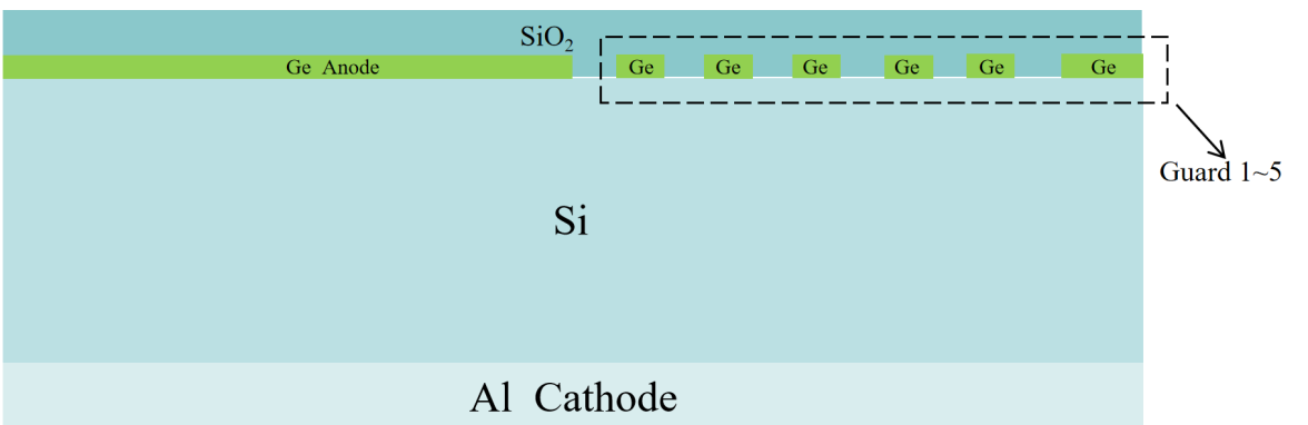
Figure 1: PIN protection ring detector structure
3. Device simulation
In order to study the role of guard rings in electric field shaping and breakdown suppression, simulations were performed using TCAD Silvaco software. In the same way as the symmetric structure of the sensor, the edge part of the sensor is selected for the construction and study of the simulation model[10-11]. The details are as follows:
3.1. Definition of structure width
The device is constructed with a multi-stage gradient guard rings system in the lateral dimension, with the anode region having a width of 3000 μm, followed by four guard rings with a width of 50 μm (GR1-GR4) in sequence, and the inter-ring spacing adopting a gradient decreasing design of 50-50-50-50-50-100 μm, and finally a 100 μm-width ground ring as the terminal structure. The longitudinal stacking structure is in order from surface to substrate: 0.2 μm thick SiO₂ passivation layer, 0.1 μm thick P+ type germanium functional layer (doping concentration of 1×1020cm-³), and 500 μm thick N-type silicon substrate (resistivity of 10 10 kΩ·cm). The germanium layer forms the anode and guard rings region through a patterning process, and the backside of the silicon substrate achieves ohmic contact through a full-area aluminum electrode.
3.2. Meshes
The device simulation in this study adopts a non-uniform meshing technique, which realizes the balance between computational accuracy and efficiency through the gradient control of spatial resolution. In the lateral (x-direction) dimension, the meshing strategy is dynamically adjusted based on the electric field distribution characteristics: the right edge of the anode region (2950-3000 μm range) is set to be divided with the highest precision and the mesh spacing is 1.67 μm (i.e., gap1_wid/30) in order to accurately characterize the carrier injection behavior at the metal-semiconductor contact interface; the guard rings gap region (gap1-gap5) is encrypted with progressive meshes, and the spacing is gradually refined from the initial 50 μm to 2.5 μm (gap1_wid/20) to effectively capture the electric field gradient changes at the edge of the guard rings. The longitudinal (y-direction) meshes are designed to optimize the interface between the surface functional layer and the substrate: the surface P+Ge layer (0-0.1 μm) is divided at a spacing of 0.03 μm to ensure high-precision simulation of the carrier transport process; the oxide layer (-0.2-0 μm) is divided at an equal spacing (Δy=0.2 μm), and the main body of the silicon substrate is divided at a spacing of Δy=0.2 μm. region (0.1-500 μm) is divided by equal spacing (Δy=0.2 μm), while the meshes in the main body of the silicon substrate (0.1-500 μm) are extended to 50 μm, which are automatically encrypted at the boundary of the depletion region by adaptive algorithm. The convergence validation of this meshes scheme shows that under the condition of maintaining the total number of nodes lower than 1.2×10⁵, the calculation error of the electric field strength in the critical region is controlled within 3%, which significantly improves the reliability of the breakdown voltage prediction.
3.3. Interface conditions
Optical interfaces: the first interface is the germanium layer surface (y=-poly_thk, i.e., Ge/Al contact surface), and the second interface is the semiconductor surface (y=0, i.e., Ge/SiO₂ interface). The reflectivity is all set to 0, and there is no reflection loss of photogenerated carriers at the interface.
Electrical contact interface: the cathode contact adopts the ideal contact model, full backside ohmic contact, and the material is metallic aluminum; the anode area is located at the right edge at x (2950-3000 μm), and the material is aluminum, which forms a Schottky contact with germanium.
Material interface properties: the Ge/Si heterogeneous interface is modeled using the SRH composite model, activated by model consrh.
The germanium layer carrier lifetime τ_n=τ_p=0.1 ms is significantly lower than that of the silicon substrate τ_n=τ_p=10 ms.
3.4. Solution methods
Nonlinear equation system solution method: Based on the Newton-Raphson iterative algorithm (Newton-Raphson method), a self-consistent solution framework is constructed, and the nonlinear coupling of Poisson equation and carrier continuity equation is handled by the dynamic updating of Jacobian matrix (Jacobian matrix). In the specific implementation, a maximum of 40 iterations (itlimit=40) are carried out in each voltage step, and convergence is judged when the relative deviation of the node potentials in two consecutive iterations is less than 1e-5. For the problem of sudden change of electric field caused by the structure of guard rings, the algorithm automatically activates the damping factor adjustment mechanism (damping factor=0.1-1.0), which effectively suppresses the numerical oscillation under high bias voltage.
Physical model coupling mechanism: The simulation process integrates multiple physical effects such as SRH complex (consrh), Oechsche complex (auger), Fermi statistics (fermi) and concentration-dependent mobility (commob). The carrier transport model is solved by solving the drift-diffusion equation in conjunction with the quantum mechanical correction term (bgn term describes the bandgap shrinkage effect induced by high doping), and the discretization process adopts the Scharfetter-Gummel format to ensure the numerical stability. For the carrier dynamics at the guard rings/substrate interface, the algorithm realizes the accurate capture of the transient response through adaptive time-step control (not explicitly defined, default Δt=1e-12 s).
Staged voltage scanning strategy: a progressive bias loading scheme (0 V → 50 V → 200 V → 400 V) is adopted, with voltage steps of 1 V and 2 V. The strategy improves computational robustness through a two-step convergence guarantee mechanism: firstly, the quasi-thermal equilibrium initial conditions are established in the low bias region (<50 V), and subsequently, the avalanche breakdown model is activated in the high bias region (triggered by a collisional ionization integration threshold). The simulation data output contains the complete field distribution and energy band information of the three eigenstate points (50 V, 200 V, 400 V), which provides a multi-scale observation window for breakdown characterization.
4. Device performance analysis
4.1. I-V curve
As shown in Fig. 2, this I-V curve demonstrates the Cathode Current-Anode Voltage characteristics of the PIN guard rings diode in reverse bias under no-light conditions. In reverse bias, the width of the depletion region increases, the diffusion of carriers is suppressed, and the reverse current is very close to zero, mainly determined by the drift motion of the minority carriers; in forward bias, the potential barrier of the PN junction decreases, the diffusion motion of carriers is enhanced, and the sharp drop in the breakdown region (0.8-3.5 V) corresponds to avalanche breakdown, and the current increases rapidly With further increase in voltage, the current tends to saturation.
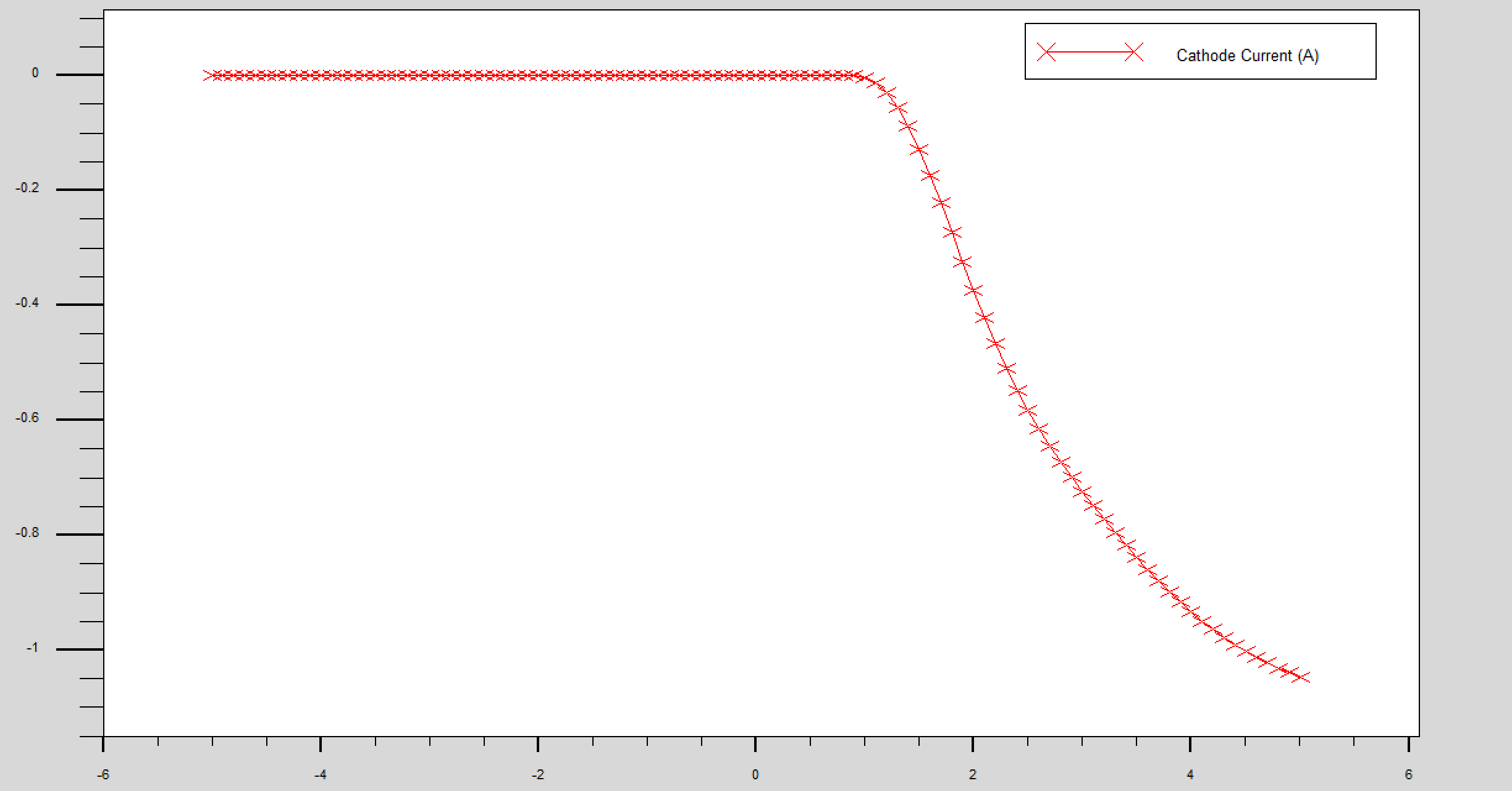
Figure 2: Cathode current-anode voltage diagram in non-illumination condition
4.2. Potential energy distribution
The overall potential distribution of the device is illustrated in Fig. 3, and Fig. 4 shows the tangent plot at y = 0.2 μm in Figure 3, covering the range from the anode region to the guard rings system (0-3800 μm). In the transverse direction, the potential gradient increases significantly in the anode region (at x ≈ 3000 μm), which corresponds to the strong electric field region at the edge of the PN junction depletion region. The potential rises from the anode contact point (x=3000 μm) with an overall nonlinear increasing trend. It is noteworthy that the potential rise rate slows down significantly at the guard ring gap (e.g., x=3100-3150 μm), indicating that the guard rings reduce the electric field concentration effect by extending the depletion region width.
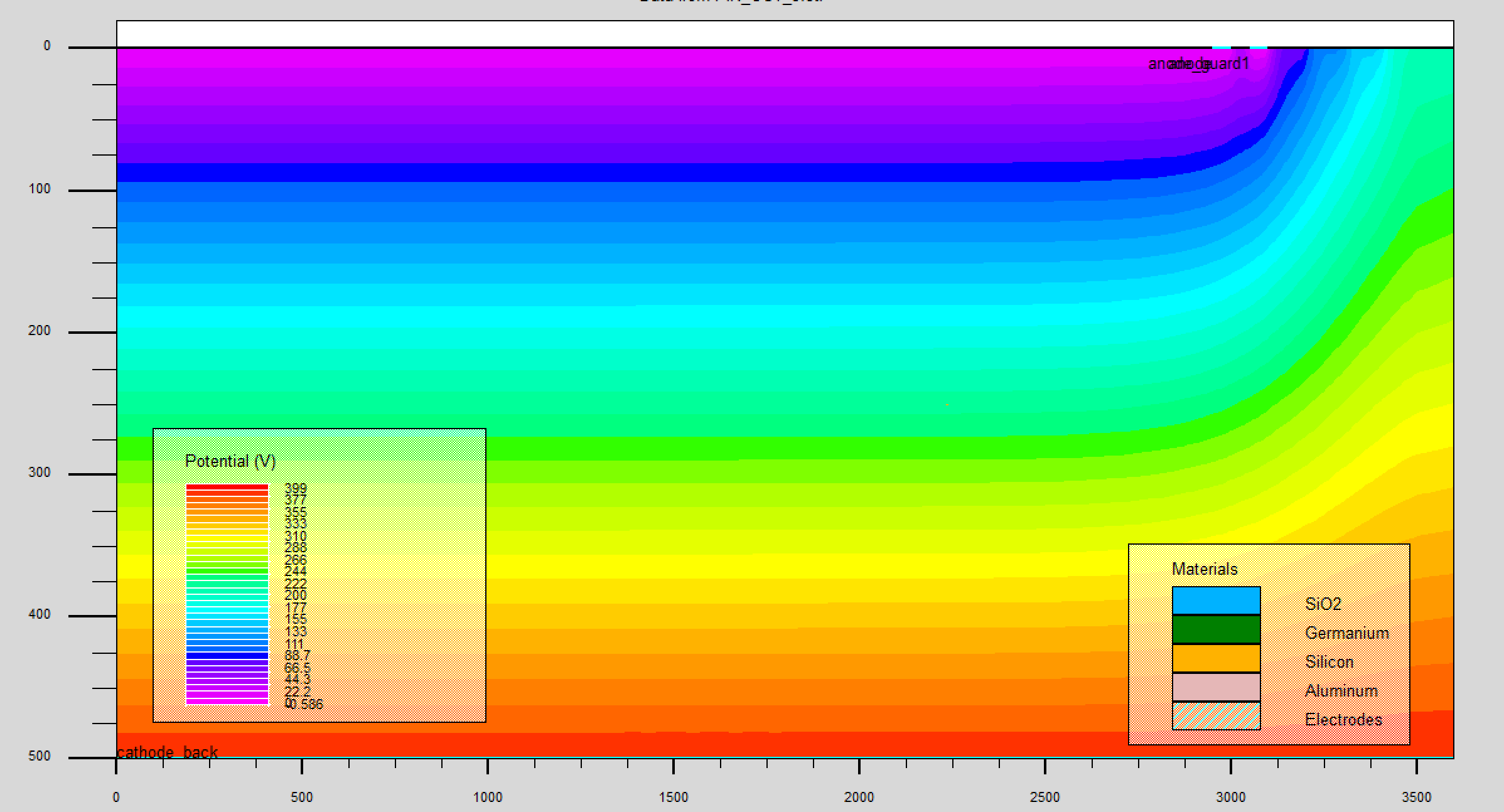
Figure 3: Potential distribution of PIN detector
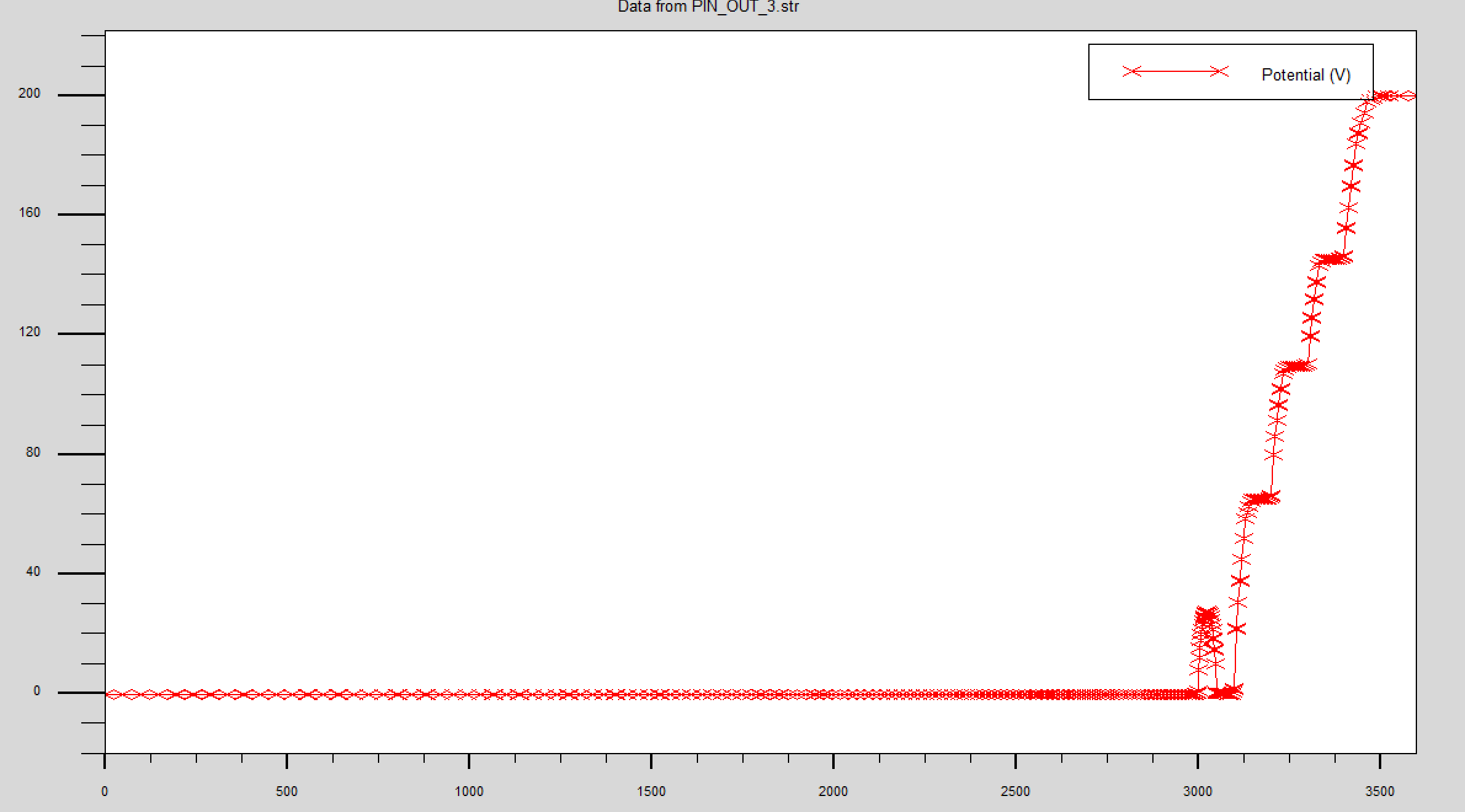
Figure 4: Potential tangential diagram at y=0.2μm
4.3. Electric field distribution
Fig. 5 shows the electric field distribution of the whole detector, overall the electric field distribution is relatively uniform, the electric field strength is low in most areas, the electric field strength fluctuates significantly at the right edge, and the strong electric field is mainly concentrated near the electrode. Fig. 6 focuses on the tangent plot of the electric field at y = 0.2 μm, including the electric field distribution in the anode-protection ring transition zone (x = 3000-3800 μm), and the maximum electric field strength reaches 6 × 10⁴ V/cm, which occurs at the right edge of the anode zone (x ≈ 3100 μm). The E-field intensity in the gap between the guard rings showed a stepwise decrease, and the four levels of guard rings suppressed the peak E-field to 1.2 × 10⁴ and 9 × 10³ and V/cm, respectively, which verified the effectiveness of the gradient spacing design. The electric field intensity drops to near 2 × 10³ V/cm before the grounded ring (x ≈ 3600 μm), indicating that the guard rings structure successfully avoids the risk of edge breakdown.
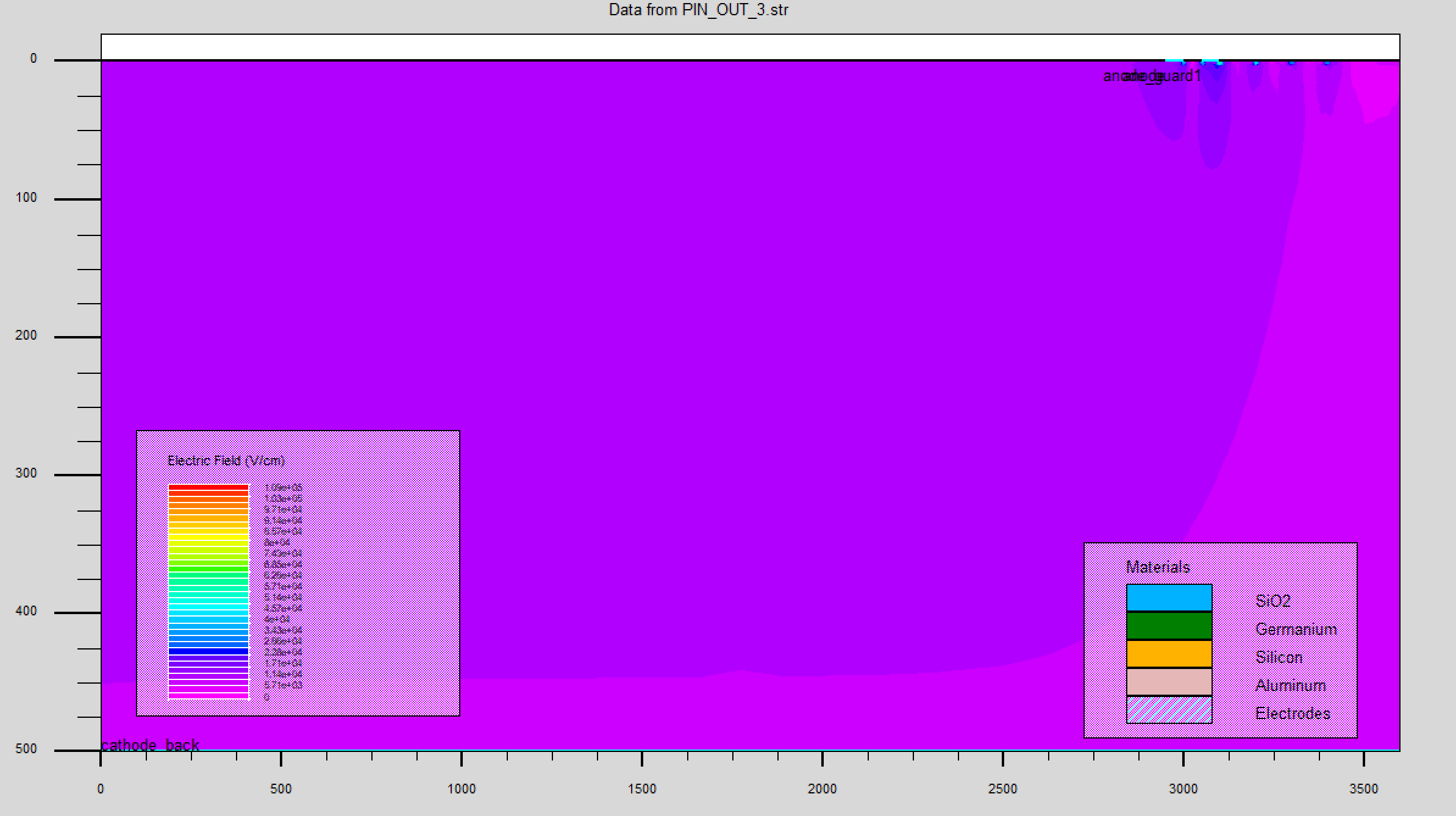
Figure 5: Electric field distribution of PIN detector
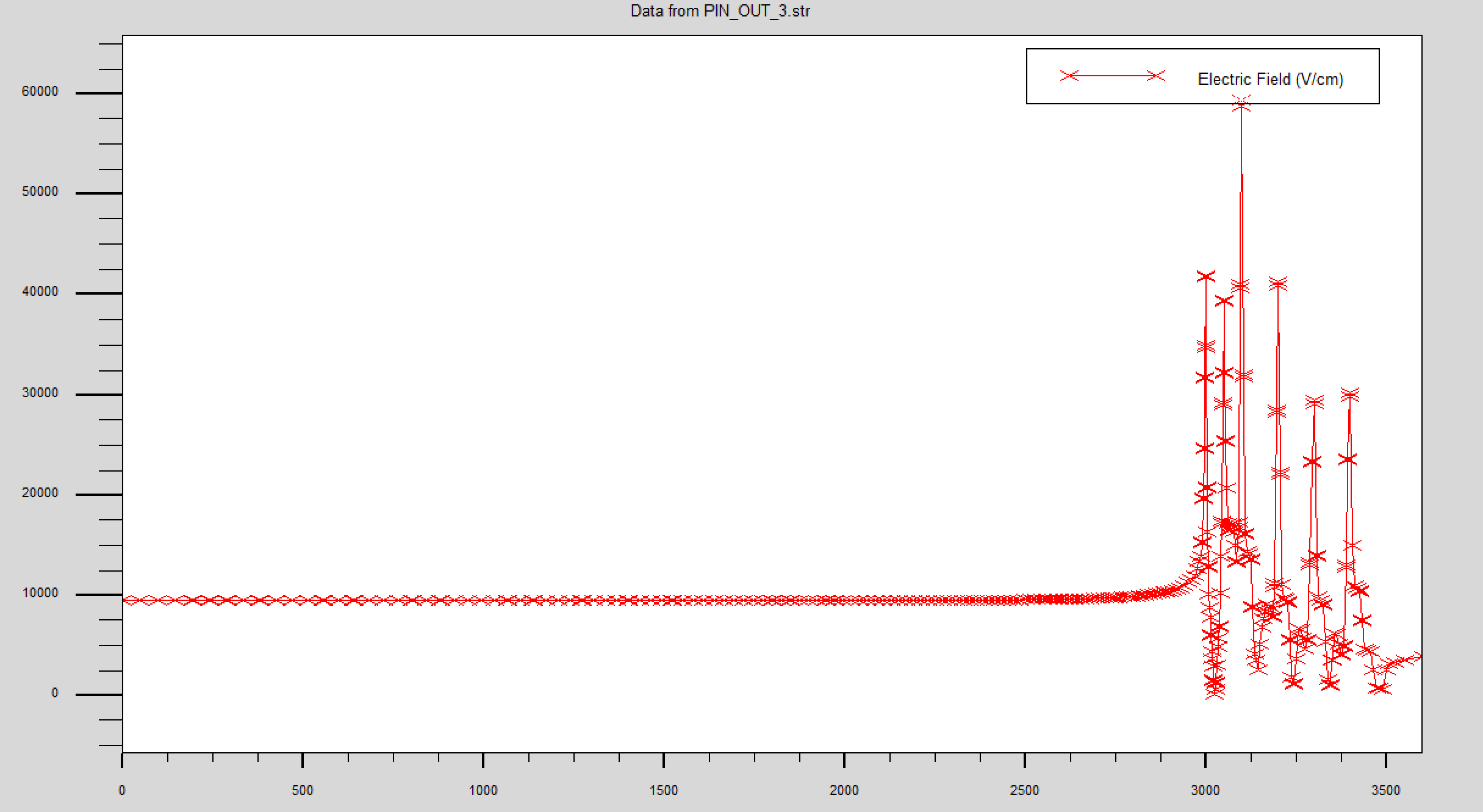
Figure 6: Tangential diagram of electric field at y=0.2μm
5. Conclusion
This study focuses on the performance optimization of silicon-based PIN guard ring detectors. TCAD Silvaco software was used to simulate the silicon-based PIN guard ring detectors, focusing on the role of the guard rings in electric field shaping and breakdown suppression. The lateral and vertical structures of the device were optimized by constructing a multilevel gradient guard rings system. A non-uniform meshing technique is adopted in the simulation to ensure high-precision modeling of critical regions, while the nonlinear coupling of Poisson's equation and carrier continuity equation is solved by the Newton-Raphson iterative algorithm.
The I-V curves demonstrate the current-voltage characteristics of the device under reverse bias and forward bias. In reverse bias, the current is very close to zero, which is mainly determined by the drift motion of the minority carriers; in forward bias, the current increases rapidly, and the sharp decrease in the breakdown region corresponds to the avalanche breakdown effect; the potential starts to rise from the anode contact point, with an overall nonlinear rising trend. The rising rate of potential at the gap of the guard rings slows down significantly, indicating that the guard rings reduce the electric field concentration effect by expanding the width of the depletion region; the electric field concentrates near the electrodes, and the electric field strength of the gap of the guard rings shows a stepwise decrease, which verifies the validity of the gradient spacing design. The maximum E-field intensity occurs at the right edge of the anode region, and the guard rings structure successfully avoids the risk of edge breakdown.
Multi-physics model coupling simulation: integrating multiple physical effects such as SRH complex, Oechs compound, Fermi statistics and concentration-dependent mobility to accurately capture the carrier dynamics process; high-precision meshes: adopting non-uniform mesh delineation technology ensures high-precision simulation of the critical region and improves the computational efficiency at the same time; gradient guard rings design: through the design of the multi-stage gradient guard rings system, it significantly reduces the edge The design of the gradient protection ring system significantly reduces the concentration of electric field at the edge and effectively suppresses the breakdown effect.
This study shows that the PIN guard rings structure significantly improves the breakdown resistance of the detector and optimizes the shaping of the edge electric field. Future research will further explore the application of new materials and structural design of guard rings to further improve the breakdown voltage, sensitivity and signal-to-noise ratio of the devices.
References
[1]. Ferrero, Marco, et al. An Introduction to Ultra-Fast Silicon Detectors. CRC press, 2021.
[2]. Jursinic, Paul. "A PIN photodiode ionizing radiation detector with small angular dependence and low buildup." Radiation Measurements 166 (2023): 106963.
[3]. Cai, Qing, et al. "Progress on AlGaN-based solar-blind ultraviolet photodetectors and focal plane arrays." Light: Science & Applications 10.1 (2021): 94.
[4]. Zhu, Zhiyuan, et al. "Bonding Processing and 3D Integration of High-Performance Silicon PIN Detector for ΔE-E telescope." Processes 11.2 (2023): 627.
[5]. Holmes, Jason, et al. "Performance of 5-μm PIN diamond diodes as thermal neutron detectors." Nuclear Instruments and Methods in Physics Research Section A: Accelerators, Spectrometers, Detectors and Associated Equipment 961 (2020): 163601.
[6]. Othman, Mohd Azlishah, et al. "Performance analysis of InGaAs/InP avalanche photodiode by using different guard ring structures." AIP Conference Proceedings. Vol. 1586. No. 1. American Institute of Physics, 2014.
[7]. Zhang, Sinuo, et al. "Breakdown performance of guard ring designs for pixel detectors in 150 nm CMOS technology." Nuclear Instruments and Methods in Physics Research Section A: Accelerators, Spectrometers, Detectors and Associated Equipment 1063 (2024): 169287.
[8]. Oomme, Roshni, and Merin K. Georg. "Performance analysis of guard ring based photodiode." Materials Today: Proceedings 43 (2021): 3701-3705.
[9]. Tabbett, Justin, and Karen L. Aplin. "Modelling the response of a CsI (Tl)-PiN photodiode Microscintillator detector." Nuclear Instruments and Methods in Physics Research Section A: Accelerators, Spectrometers, Detectors and Associated Equipment 1061 (2024): 169105.
[10]. Croci, T., et al. "Advances in the TCAD modelling of non-irradiated and irradiated Low-Gain Avalanche Diode sensors." Journal of Instrumentation 19.01 (2024): C01022.
[11]. Croci, Tommaso, et al. "Measurements and TCAD simulations of guard-ring structures of thin silicon sensors before and after irradiation." Nuclear Instruments and Methods in Physics Research Section A: Accelerators, Spectrometers, Detectors and Associated Equipment 1069 (2024): 169801.
Cite this article
Yu,C. (2025). Optimization and Design of Silicon PIN Detector Guard Ring Structure. Applied and Computational Engineering,162,105-111.
Data availability
The datasets used and/or analyzed during the current study will be available from the authors upon reasonable request.
Disclaimer/Publisher's Note
The statements, opinions and data contained in all publications are solely those of the individual author(s) and contributor(s) and not of EWA Publishing and/or the editor(s). EWA Publishing and/or the editor(s) disclaim responsibility for any injury to people or property resulting from any ideas, methods, instructions or products referred to in the content.
About volume
Volume title: Proceedings of CONF-FMCE 2025 Symposium: Semantic Communication for Media Compression and Transmission
© 2024 by the author(s). Licensee EWA Publishing, Oxford, UK. This article is an open access article distributed under the terms and
conditions of the Creative Commons Attribution (CC BY) license. Authors who
publish this series agree to the following terms:
1. Authors retain copyright and grant the series right of first publication with the work simultaneously licensed under a Creative Commons
Attribution License that allows others to share the work with an acknowledgment of the work's authorship and initial publication in this
series.
2. Authors are able to enter into separate, additional contractual arrangements for the non-exclusive distribution of the series's published
version of the work (e.g., post it to an institutional repository or publish it in a book), with an acknowledgment of its initial
publication in this series.
3. Authors are permitted and encouraged to post their work online (e.g., in institutional repositories or on their website) prior to and
during the submission process, as it can lead to productive exchanges, as well as earlier and greater citation of published work (See
Open access policy for details).
References
[1]. Ferrero, Marco, et al. An Introduction to Ultra-Fast Silicon Detectors. CRC press, 2021.
[2]. Jursinic, Paul. "A PIN photodiode ionizing radiation detector with small angular dependence and low buildup." Radiation Measurements 166 (2023): 106963.
[3]. Cai, Qing, et al. "Progress on AlGaN-based solar-blind ultraviolet photodetectors and focal plane arrays." Light: Science & Applications 10.1 (2021): 94.
[4]. Zhu, Zhiyuan, et al. "Bonding Processing and 3D Integration of High-Performance Silicon PIN Detector for ΔE-E telescope." Processes 11.2 (2023): 627.
[5]. Holmes, Jason, et al. "Performance of 5-μm PIN diamond diodes as thermal neutron detectors." Nuclear Instruments and Methods in Physics Research Section A: Accelerators, Spectrometers, Detectors and Associated Equipment 961 (2020): 163601.
[6]. Othman, Mohd Azlishah, et al. "Performance analysis of InGaAs/InP avalanche photodiode by using different guard ring structures." AIP Conference Proceedings. Vol. 1586. No. 1. American Institute of Physics, 2014.
[7]. Zhang, Sinuo, et al. "Breakdown performance of guard ring designs for pixel detectors in 150 nm CMOS technology." Nuclear Instruments and Methods in Physics Research Section A: Accelerators, Spectrometers, Detectors and Associated Equipment 1063 (2024): 169287.
[8]. Oomme, Roshni, and Merin K. Georg. "Performance analysis of guard ring based photodiode." Materials Today: Proceedings 43 (2021): 3701-3705.
[9]. Tabbett, Justin, and Karen L. Aplin. "Modelling the response of a CsI (Tl)-PiN photodiode Microscintillator detector." Nuclear Instruments and Methods in Physics Research Section A: Accelerators, Spectrometers, Detectors and Associated Equipment 1061 (2024): 169105.
[10]. Croci, T., et al. "Advances in the TCAD modelling of non-irradiated and irradiated Low-Gain Avalanche Diode sensors." Journal of Instrumentation 19.01 (2024): C01022.
[11]. Croci, Tommaso, et al. "Measurements and TCAD simulations of guard-ring structures of thin silicon sensors before and after irradiation." Nuclear Instruments and Methods in Physics Research Section A: Accelerators, Spectrometers, Detectors and Associated Equipment 1069 (2024): 169801.