


1. Introduction
An integrated circuit (IC) is an electronic circuit that integrates many microelectronic elements, including transistors, diodes, capacitors, resistors, inductors, etc. using a specific process. Compared with traditional electronic components, ICs have the advantages of high integration and smaller size.
As early as around 1952, Geoff Dummer put forward the idea of concentrating independent electronic components on semiconductor chips, and proposed a specific circuit design scheme [1]. In 1958, Jack Kilby successfully integrated multiple germanium devices on a single wafer [2]. This is the first IC in the world, for which he won the Nobel Prize in physics. From the invention of ICs to the proposition of Moore's Law in 1965 [3], people's design level of ICs is getting higher and higher. After that, the research and development of chips has developed rapidly, and better results have been achieved gradually. The size of IC technology has also entered the nanometer level.
As the integration and complexity of chips become higher, the reliability problem of devices becomes more prominent. Even on a chip with tens of thousands of devices or more, the logic output of a few devices is chaotic or delayed, which will greatly affect the function of the chip. Therefore, the reliability problem has become a major bottleneck in the development of very large integration integration (VLSI) [4].
This paper mainly discusses the reliability of complementary metal oxide semiconductor (CMOS) circuits. Due to the advantages of low power consumption, high integration and high working speed, CMOS circuits have been widely used in ICs. However, after the CMOS circuit technology enters the deep sub-micron stage, the impact of various reliability issues on ICs is more prominent. If the designed device does not have high reliability in the normal use stage, it will cause irregular failure due to the change of external environmental factors such as temperature, humidity, working voltage, etc., thus causing the circuit logic to change to the normal working state and causing the logic error at the circuit output.
At present, the reliability problems that have great influence on CMOS devices include negative-bias temperature instability (NBTI) [5], electromigration (EM) [6], time-dependent gate oxide breakdown (TDDB) [7] and hot carrier injection (HCI) [8]. This paper first briefly introduces these four kinds of reliability problems, and then analyzes the causes of the reliability problems. Finally. This paper summarizes the existing solutions for different reliability problems.
2. CMOS reliability issues
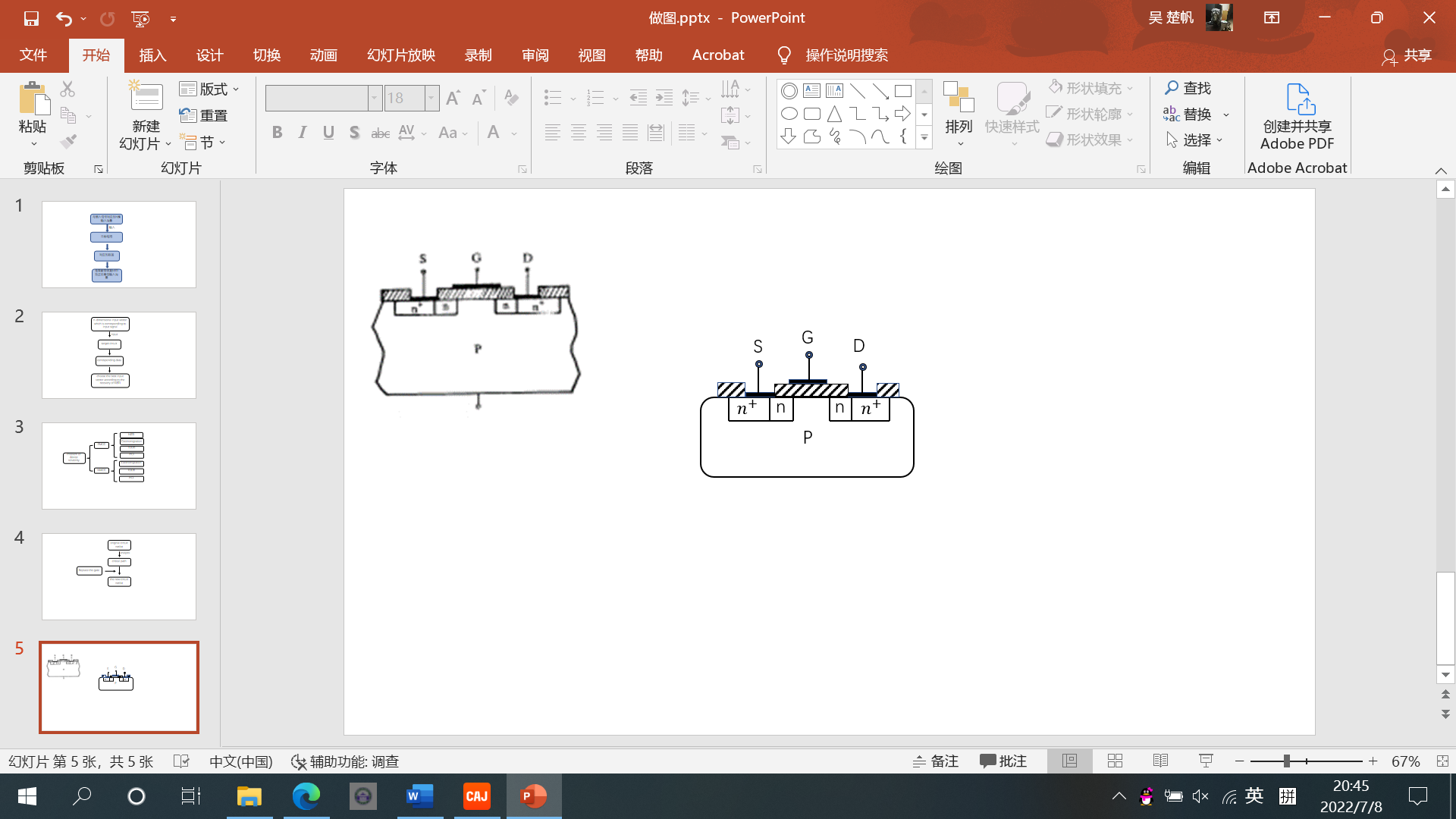
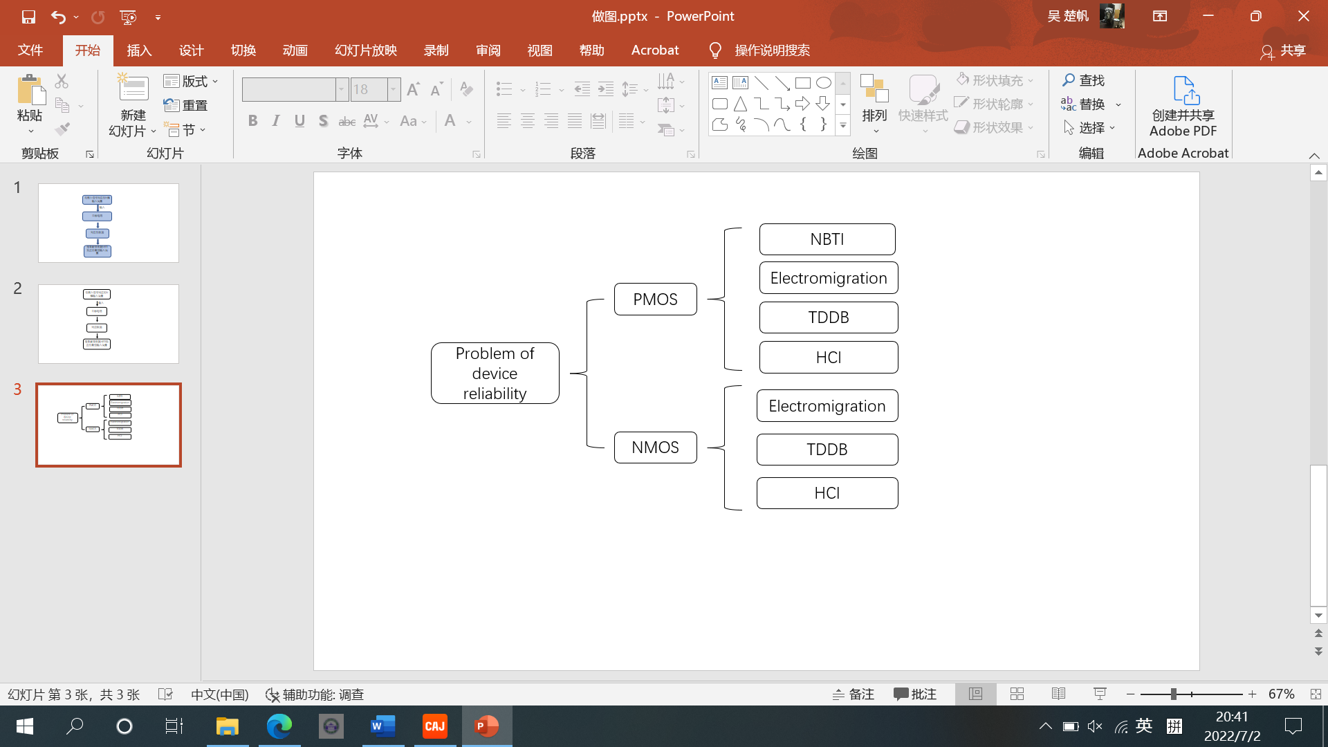 CMOS devices can be divided into N-Metal-Oxide-Semiconductor (NMOS) and positive channel metal oxide semiconductor (PMOS) devices according to the different materials used for the substrate, source and drain. NMOS uses a P-type silicon substrate and PMOS uses an N-type silicon substrate. As shown in fig. 1, both CMOS devices have reliability problems, but for NMOS devices, the NBTI effect is very weak, so it will not affect the data of the devices.
Fig. 1 Reliability Issues in CMOS Circuits
2.1. NBTI effect
NBTI refers to the device degradation phenomenon of metal–oxide–semiconductor field-effect transistor (MOSFET) under high temperature and negative gate bias, which is mainly manifested by the increase of absolute value of threshold voltage and the decrease of mobility, leakage current and transconductance of PMOS transistors. The effect of this effect on the NMOS transistor is negligible.
The generation of NBTI effect is due to the electrochemical reaction between H2 and H2O introduced in the process of semiconductor manufacturing and used at the interface of Si-SiO2, which results in the generation of trap charge and interface state charge in the oxide layer, thus changing the parameters of the device.
The early research on NBTI effect mainly focused on the establishment of NBTI analysis model and its influence on various electrical parameters of transistors [9]. Bhardwaj et al. proposed a reaction-diffusion model to deal with NBTI [10]. Based on the reaction diffusion model, Wang et al. proposed the shift of threshold voltage in PMOS transistors under static and dynamic NBTI effects, and derived their mathematical model [11].
2.2. HCI effect
A transverse electric field exists in the MOSFET device during operation. Under the action of transverse electric field, carriers in the channel are accelerated, and some accelerated carriers obtain high energy and become hot carriers.
Under the action of HCI, the threshold voltage of the NMOS transistor increases and the drain current decreases, resulting in an increase in the charge and discharge time of the NMOS transistor. However, the absolute value of the threshold voltage of the PMOS transistor decreases and the drain current increases, resulting in a decrease in the PMOS charge-discharge time. Therefore, in the CMOS logic circuit, under the action of HCI, the time for the circuit node level to flip up and down is asymmetric, resulting in signal advance when rising from low level to high level and signal delay when falling from high level to low level.
With the in-depth study of HCI effect, some scholars have continuously proposed new HCI mechanisms, such as secondary hot electron injection, substrate hot electron injection and so on [12] [13]. In practical MOSFET devices, there are many HCI mechanisms.
2.3. EM effect
EM refers to the phenomenon that metal ions in metal conductor materials migrate under the action of a large number of electronic movements.
At the grain boundary in the metal structure, the order of the lattice structure is broken and the kinetic energy exchange between ions is more frequent. The metal atoms at the grain boundaries are much less bound than in a uniform lattice. When a large number of electrons move and the electron wind reaches a certain intensity, the metal atoms gradually move away from the grain boundaries towards the direction of electron movement.
When EM occurs in CMOS ICs, the metal material deviates from its original position, causing local metal lines to narrow or voids to form. When the metal wire carries large current, the increased resistance makes the thermal effect of current more obvious, and the increase of metal wire temperature further intensifies the occurrence of EM. As the EM effect intensifies, the metal lines eventually break, causing unrecoverable circuit failures. When EM occurs between two adjacent metals, the outward diffusion of metal substances may cause a short circuit between the two metals, resulting in the failure of the circuit.
2.4. TDDB effect
TDDB refers to the breakdown phenomenon that occurs when the dielectric layer is in a state of stress lower than the intrinsic breakdown voltage for a long time. Because this phenomenon mostly occurs in the gate oxide layer of MOSFET, it is also called gate oxide breakdown. When the gate oxide layer breaks down, a gate current is generated. When the gate current is small and is equivalent to the gate oxide barrier penetration current, the electrical characteristics of the MOSFET remain basically unchanged, and breakdown at this time is called soft breakdown. When the gate current is large, the thermal effect caused by the large current causes irreversible breakdown of the gate oxide layer, which is called hard breakdown.
3. CMOS circuit reliability solutions
3.1. Resolution of NBTI Effect
The gate replacement method is based on the self-recovery mechanism of NBTI effect. By inserting a transmission gate and a transistor into the protected gate in the circuit sleep (static) mode, the purpose of relieving the circuit aging is achieved. The flow is shown in Figure 2. However, due to the introduction of additional transistors, this approach will bring more area overhead.
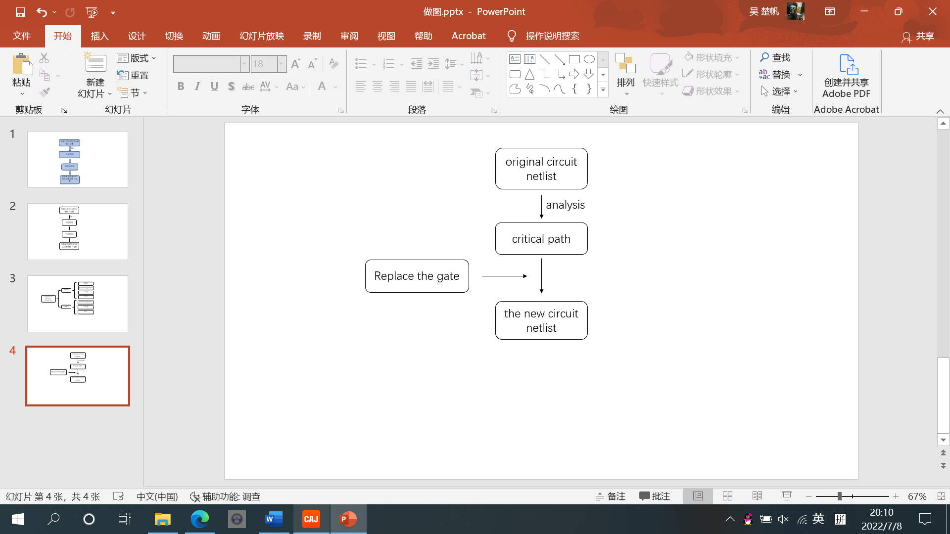 The specific method is to replace the door opening of the door which is easy to age, and add a sleep signal for it. When the circuit works normally, Sleep=0, which does not affect the normal work of the circuit. when the circuit stands by, Sleep=1, which is used to relieve the aging of the circuit.
Fig. 2 Flowchart of door replacement
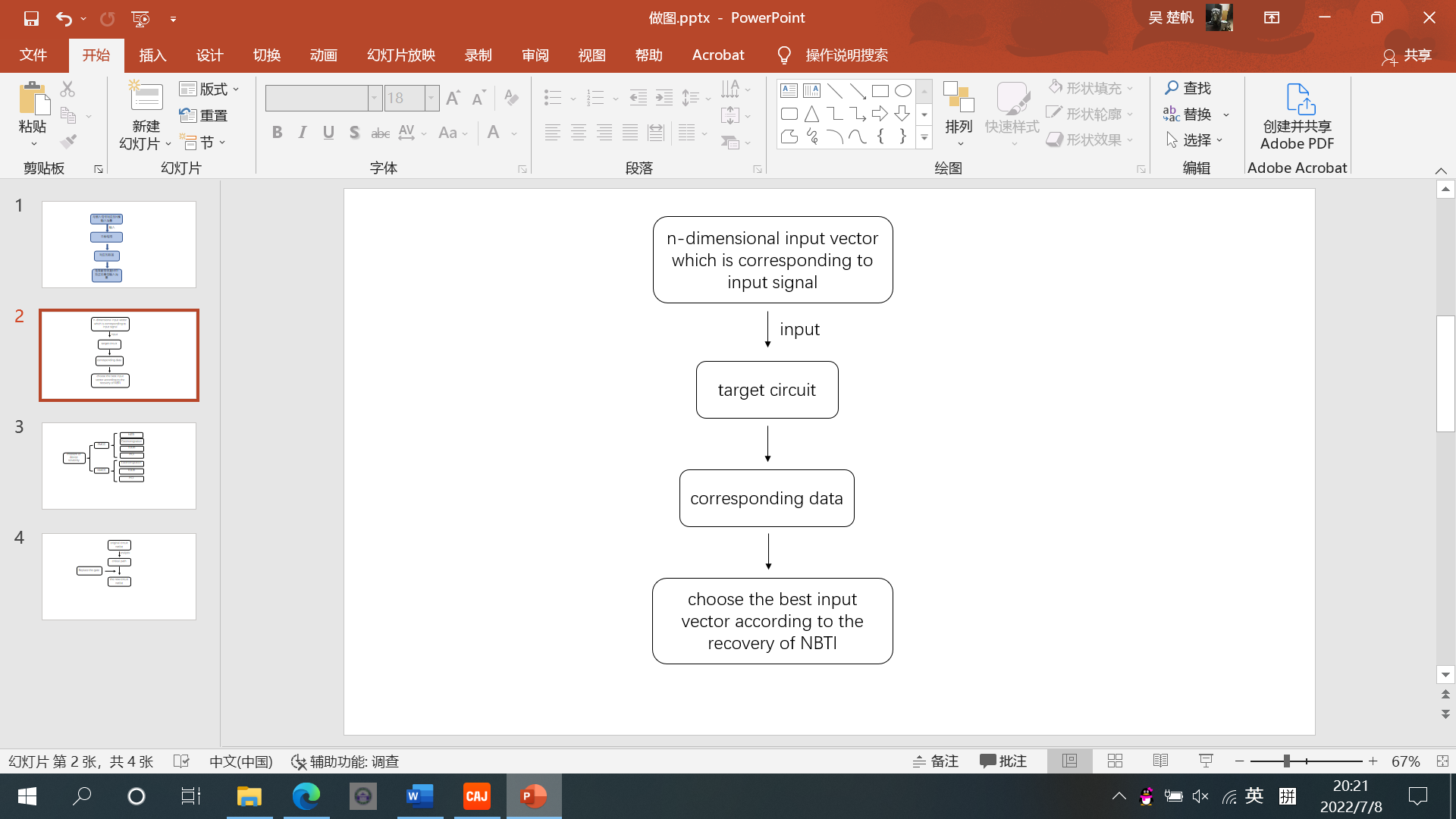 The input vector control method is to input a control vector at the input of the circuit when the circuit is on standby, so that the inputs of the aging sensitive gates in the circuit are all 1, and the circuit is in the NBTI recovery stage at this time, so as to achieve the purpose of relieving aging, as shown in Figure 3. The optimal input vector is pre-selected in the design stage of the circuit and applied to the circuit when it enters the standby mode.
Fig. 3 Flow chart of input vector control method
3.2. Methods to Reduce Hot Carrier Effect
 The hot carrier effect can be reduced by using the lightly doped drain (LDD) structure. As shown in fig. 4, a lightly doped region is formed at each of the source and drain regions connected to the channel. Due to the higher resistivity of the lightly doped region type, the applied drain-source voltage is no longer only dropped on the channel but a part is shared by the lightly doped region, which is equivalent to lengthening the channel. But the LDD structure does not substantially change the geometry of the device.
Fig. 4 Schematic Diagram of LDD Structure of NMOS
However, because the structure uses low doping, the resistance value of the drain terminal will increase, which will reduce leakage current.
In addition, the hot carrier effect can be reduced by improving the quality of the gate oxide layer. The oxidation temperature is appropriately increased. If there is sufficient chemical reaction between oxygen and silicon at the Si-SiO2 interface, the interface state formed by silicon dangling bonds will be greatly reduced. On the other hand, higher oxidation temperature can further activate silicon and oxygen, which is beneficial to silicon-oxygen bonding, thus reducing non-bridging ions in the network structure, improving the density of the network structure and reducing the number of defects. The decrease of interface state and defects in gate oxide will weaken the degeneration of parameters such as transconductance caused by hot carriers.
Nitriding the gate oxide layer can also reduce the number of defects in the oxide layer. Moreover, the nitrogen accumulated at the Si-SiO2 interface can reduce the interface stress and achieve the purpose of reducing the interface state density. Since the binding energy of the N-Si bond is higher than that of the Si-H bond, it is more difficult to break the N-Si bond when hot electrons are injected into the oxide layer.
3.3. Factors affecting EM
Different shapes and structures of interconnection leads can change the distribution of current density. For example, the uneven distribution of current density at the corner of the lead leads to a larger current density gradient at 90 angles than at 45 and 30 angles, which results in an increase in vacancy current increment and a more significant EM phenomenon.
Temperature affects the EM process by affecting the diffusion of atoms in the interconnect leads. The diffusion coefficient D of atoms in the interconnect leads is exponentially related to temperature. When the temperature increases, the diffusion speed of atoms increases. If there is a temperature gradient on the interconnection leads, there will be differences in atomic diffusion coefficients of some structures on the interconnection leads, resulting in atomic migration.
In addition, the doped impurities can also affect the EM phenomenon. For example, Cu has good EM resistance. Adding appropriate amount of Cu in Al can effectively improve its EM resistance [14].
3.4. Factors Causing TDDB
Substrate performance is significantly affected when contaminated with metal. In addition, if Al, Fe and Ca are present on the Si surface during the oxidation process, the performance of SiO2 will also be significantly reduced. Raw materials (heavy metals precipitated in Si) or process (fixtures used in sputtering, implantation process; chemical reagents) can introduce metal contamination.
When the silicon single crystal is grown by the CZ method, it contains oxygen atoms. These oxygen atoms may cause bulk defects, thus reducing the integrity of the gate oxygen and ultimately deteriorating the quality of the substrate which is prone to TDDB.
4. Conclusion
With the continuous development and maturity of IC manufacturing technology, the research on the reliability of CMOS devices has become particularly important. Although there are many reliability problems in CMOS devices, such as NBTI, EM, TDDB, HCI and so on, for different problems, we can take measures such as changing circuit structure, selecting appropriate input vectors, improving material quality, improving production line environment and so on to alleviate them. This is of great help to the technological development of ICs and the reduction of the development cost of ICs.
References
[1]. Green, M. . "Dummer's Vision of Solid Circuits at the UK Royal Radar Establishment." Annals of the History of Computing, IEEE 35.1(2013):56-66.
[2]. ECKSTEIN PETER. Jack Kilby (1923-2005)[J]. IEEE annals of the history of computing,2007,29(1):90-95.
[3]. Moore.G.E.,Electronics,1965;38(8):114-117.
[4]. G. Groeseneken, R. Degraeve, et al. Challenges in reliability assessment of advanced CMOS technologies[C]. Proceedings of Physical and Failure Analysis of Integrated Circuits, India, 2007, 1-9
[5]. Stathis, J. H. , and S. Zafar . "The negative bias temperature instability in MOS devices: A review." Microelectronics Reliability 46.2/4(2006):270-286.
[6]. Allan, A. "International Technology Roadmap for Semiconductors (ITRS)." Journal of Applied Physics 86.17(2015):045406.
[7]. Schlund, B. , et al. "A new physics-based model for time-dependent-dielectric-breakdown." IEEE 1995 International Integrated Reliability Workshop. Final Report IEEE, 1995.
[8]. Chenming, et al. "Hot-electron-induced MOSFET degradation—Model, monitor, and improvement." Electron Devices IEEE Transactions on (1985).
[9]. Srinivasan, J. , et al. "The Impact of Technology Scaling on Lifetime Reliability." Dependable Systems and Networks, 2004 International Conference on IEEE, 2004.
[10]. Bhardwaj, S. , et al. "Predictive Modeling of the NBTI Effect for Reliable Design." Custom Integrated Circuits Conference, 2006. CICC '06. IEEE IEEE, 2006.
[11]. Wang, W. , et al. "The Impact of NBTI on the Performance of Combinational and Sequential Circuits." IEEE Design Automation Conference IEEE, 2007.
[12]. Takeda E, Suzuki N. An empirical model for device degradation due to hot-carrier injection[J]. Electron Device Letters, IEEE, 1983, 4(4): 111-113.
[13]. Hu C, Tam S C, Hsu F C, et al. Hot-electron-induced MOSFET degradation—Model, monitor, and improvement[J]. Electron Devices, IEEE Transactions on, 1985, 32(2): 375-385.
[14]. Liu, X. Y , C. L. Liu , and L. J. Borucki . "A new investigation of copper\"s role in enhancing Al–Cu interconnect electromigration resistance from an atomistic view." 47.11(1999):3227-3231.
Cite this article
Wu,C. (2023). Research on reliability of complementary metal oxide semiconductor integrated circuit. Applied and Computational Engineering,7,8-13.
Data availability
The datasets used and/or analyzed during the current study will be available from the authors upon reasonable request.
Disclaimer/Publisher's Note
The statements, opinions and data contained in all publications are solely those of the individual author(s) and contributor(s) and not of EWA Publishing and/or the editor(s). EWA Publishing and/or the editor(s) disclaim responsibility for any injury to people or property resulting from any ideas, methods, instructions or products referred to in the content.
About volume
Volume title: Proceedings of the 3rd International Conference on Materials Chemistry and Environmental Engineering (CONF-MCEE 2023), Part II
© 2024 by the author(s). Licensee EWA Publishing, Oxford, UK. This article is an open access article distributed under the terms and
conditions of the Creative Commons Attribution (CC BY) license. Authors who
publish this series agree to the following terms:
1. Authors retain copyright and grant the series right of first publication with the work simultaneously licensed under a Creative Commons
Attribution License that allows others to share the work with an acknowledgment of the work's authorship and initial publication in this
series.
2. Authors are able to enter into separate, additional contractual arrangements for the non-exclusive distribution of the series's published
version of the work (e.g., post it to an institutional repository or publish it in a book), with an acknowledgment of its initial
publication in this series.
3. Authors are permitted and encouraged to post their work online (e.g., in institutional repositories or on their website) prior to and
during the submission process, as it can lead to productive exchanges, as well as earlier and greater citation of published work (See
Open access policy for details).
References
[1]. Green, M. . "Dummer's Vision of Solid Circuits at the UK Royal Radar Establishment." Annals of the History of Computing, IEEE 35.1(2013):56-66.
[2]. ECKSTEIN PETER. Jack Kilby (1923-2005)[J]. IEEE annals of the history of computing,2007,29(1):90-95.
[3]. Moore.G.E.,Electronics,1965;38(8):114-117.
[4]. G. Groeseneken, R. Degraeve, et al. Challenges in reliability assessment of advanced CMOS technologies[C]. Proceedings of Physical and Failure Analysis of Integrated Circuits, India, 2007, 1-9
[5]. Stathis, J. H. , and S. Zafar . "The negative bias temperature instability in MOS devices: A review." Microelectronics Reliability 46.2/4(2006):270-286.
[6]. Allan, A. "International Technology Roadmap for Semiconductors (ITRS)." Journal of Applied Physics 86.17(2015):045406.
[7]. Schlund, B. , et al. "A new physics-based model for time-dependent-dielectric-breakdown." IEEE 1995 International Integrated Reliability Workshop. Final Report IEEE, 1995.
[8]. Chenming, et al. "Hot-electron-induced MOSFET degradation—Model, monitor, and improvement." Electron Devices IEEE Transactions on (1985).
[9]. Srinivasan, J. , et al. "The Impact of Technology Scaling on Lifetime Reliability." Dependable Systems and Networks, 2004 International Conference on IEEE, 2004.
[10]. Bhardwaj, S. , et al. "Predictive Modeling of the NBTI Effect for Reliable Design." Custom Integrated Circuits Conference, 2006. CICC '06. IEEE IEEE, 2006.
[11]. Wang, W. , et al. "The Impact of NBTI on the Performance of Combinational and Sequential Circuits." IEEE Design Automation Conference IEEE, 2007.
[12]. Takeda E, Suzuki N. An empirical model for device degradation due to hot-carrier injection[J]. Electron Device Letters, IEEE, 1983, 4(4): 111-113.
[13]. Hu C, Tam S C, Hsu F C, et al. Hot-electron-induced MOSFET degradation—Model, monitor, and improvement[J]. Electron Devices, IEEE Transactions on, 1985, 32(2): 375-385.
[14]. Liu, X. Y , C. L. Liu , and L. J. Borucki . "A new investigation of copper\"s role in enhancing Al–Cu interconnect electromigration resistance from an atomistic view." 47.11(1999):3227-3231.