


1. Introduction
Due to rising energy demand and depleting fossil fuel inventories, people require alternate energy sources. Photovoltaic (PV) technology is considered a cheaper and safer power source.
Single-junction crystalline silicon (c-Si) is the most common and dominant solar technology in the photovoltaic market. However, it has some obvious weaknesses, such as: low energy conversion efficiency (less than 26% for single-crystal, non-concentrator solar cells in 2017;[1]), high construction cost per unit for c-Si solar cells, sophisticated manufacturing techniques, and—most importantly—the theoretical efficiency limit, which is the Shockley-Queisser (S-Q) limit (at around 33%[2]). Finding a material with different band gaps to form a tandem architecture with the traditional c-Si solar cell is the easiest way to improve overall efficiency without abandoning silicon-based technology. In this scenario, a suitable material is the key.
The researchers have conducted many trials in pursuit of a material that is not only inexpensive but also capable of enhancing efficiency while maintaining excellent stability. In 2018, Cariou et al. established a dual junction design by integrating GaAs and GalnP (both as top sub-cells) with c-Si [3]. Essig et al. constructed a triple junction tandem solar cell with an efficiency exceeding 35% by combining a dual-junction GaAs/GalnP solar cell with a regular c-Si solar cell [4]. However, using expensive scarce elements is the largest impediment to mass-producing tandem cells. Therefore, the emergence of chalcogenide perovskite, primarily BaZrS3, gives tandem cells hope for the future.
Due to the limited research on BaZrS3, its thin film was considered incompatible with tandem solar cells since its bulk crystal formation likely required a high temperature. Nevertheless, this conclusion may not be accurate. Therefore, we will examine the applications of BaZrS3 in tandem solar cells and subsequently address the misconceptions around its crystallization. Finally, the crucial step-thin film growth will be explained in order to create a blueprint for its potential commercialization.
2. Categories of Tandem Structures
We must first identify the similarities and differences between a number of typical tandem device configurations in order to comprehend the criteria for appropriate material for the sub-cell.
Tandem structures can generally be divided into Type-A and Type-B categories. These two sorts of structures' functions serve as the basis for this categorization. Large-scale production is best suited for Type-A structures, whereas R&D purposes are best served by Type-B structures.
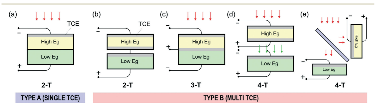
Figure 1. Brief schematic diagram of different configurations of tandem solar cells. a) Monolithically stacked with two terminals, (b) Mechanically stacked with two terminals, (c) Monolithically stacked with three terminals, (d) Mechanically stacked with four terminals, and (e) Spectrum-split with four terminals.
With a single interface layer placed between two absorption layers of material and a transparent conductive electrodes (TCE) layer on top, Type-A tandem devices (Figure 1.a) have a monolithic construction that often results in a two-terminal (2-T) solar cell device. However, it is very difficult to do research and develop on this setup since it is an entire bulk. And it can offer significant advantages in terms of commercialization and perfect scalability, since it requires only a minimal number of manufacturing procedures and materials.
By producing individual devices separately and mechanically stacking them together into 2-T, 3-T, and 4-T structures (Figure 1.b-e), the Type-B structure maximizes processing tolerance and simplifies the characterization process of the corresponding devices. With the sacrifice of its scalability, the abovementioned characteristics make the Type-B device an excellent candidate for research and feasibility testing [5].
2.1. Requirements of Tandem Cells Optimization
This section focuses on tandem architectures and bandgaps in the selection of top sub-cells. Each tandem structure computation selects a single junction c-Si with a bandgap Eg1=1.1eV as the bottom sub-cell, whereas the bandgap of the top sub-cell Eg2 is independent. The efficiency of the top and bottom sub-cells is set to be the S-Q limit of each cell in order to forecast the theoretical trends related to Eg2. In this scenario, it is assumed that the top cell's absorption is the only optical loss that occurred during the process of incident light traveling through the top cell and reaching the bottom cell. As a result, Figure 2 displays the J-V curves and overall efficiency of the tandem devices [6].
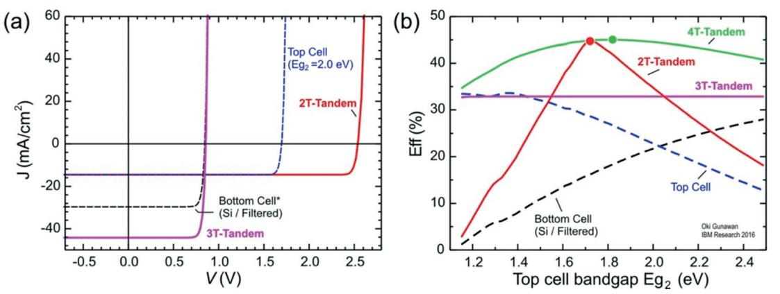
Figure 2. Performance comparison. (a) J–V curves of several tandem arrangements under AM1.5G 1 sun light condition for a top sub-cell with Eg2 = 2.0 eV (b) Efficiency curves of several tandem arrangements.
Choosing the material for the top sub-cell must consider a number of factors. First, a 2-T tandem construction has the capacity to scale perfectly while also achieving the best efficiency. The top sub-cell must be compatible with the layer beneath in order to fully benefit from these advantages. Second, the best theoretical bandgap for the top sub-cell is between 1.72eV and 1.82eV since the greatest efficiency of the 2-T and 4-T structures corresponds to the Eg2=1.72eV (2-T) and Eg2=1.82eV (4-T) values, respectively. Third, the 3-T structure is not the best arrangement for tandem solar cells because its maximum efficiency is lower than the rest and cannot be changed.
3. Theoretical Prediction of Suitable Materials for Top Sub-cell
As indicated, the top sub-cell of a tandem structure with a c-Si bottom sub-cell must have certain properties. First, its bandgap must be tunable and between 1.72eV and 1.8eV. Second, it must be compatible with interfacial layers and c-Si bottom sub-cells.
Halide perovskites are a popular choice for the top sub-cell. This type of perovskite's film deposition technique only needs 80°C to 150°C. [7]. Large-grained, extremely crystalline halide perovskite films can be formed on silicon sub-cells utilizing simple solution-based techniques. Furthermore, a low deposition temperature made it virtually impossible to harm the layers below.
The stability issue of halide perovskite materials, however, poses a significant problem. In particular, degeneration can occur at the interfaces between halide perovskite bulk and other layers. The internal structure as well as external factors such as an electric field, moisture, heat, and sunshine are the two main causes of this issue [8]. Due to the way solar cells operate, all these external factors cannot be balanced. A new photovoltaic technology must surpass or at least satisfy the stability criteria imposed by Si module makers, which is less than 10% degradation within 30 years [9], in order to be commercialized. However, even with the help of MgFx interfacial protection layers, the halide perovskite-Si tandem cell can only reach the power conversion efficiency of 95.4% after 1000hr torture test, and this is the highest stability reported [10]. This result is not good enough to support the halide perovskite on its way to commercialization.
Chalcogenide perovskites can solve the stability issue without sacrificing conversion rate. They have already demonstrated a significant potential in efficiency and other chemical or physical requirements for photovoltaic application at the early stages of research. Since very little experimental or computational information regarding telluride perovskites has been provided, the ABX3 chalcogenide perovskites with S or Se stands for X will be the focus of this study. According to calculations of structural parameters and predictions from density function theory (DFT) there is less chalcogenide perovskite than expected [11]. Chalcogenide perovskites are hence basically equivalent to sulfide perovskites. The only two examples that have the potential to be used in photovoltaics are BaZrS3 and BaHfS3.
When it comes to the promising candidate BaZrS3, the bandgap of BaZrS3 is 1.75eV [13] and 1.82eV [14]. The variation between these values may be attributed to the various proportions of Hf impurities, which are frequently present in Zr compounds. From the perspective of characterization, there is another explanation. For BaZrS3 alloys, a tiny amount of Ti or Se doping will lower the bandgap by around 0.3eV and 0.18 eV, respectively. BaZrS3 is hence appropriate for tandem photovoltaic applications. The 2.17eV bandgap BaHfS3 chalcogenide perovskite is another intriguing material. Doping alloys can be used to adjust this bandgap. However, according to DFT prediction, BaZrS3 is less stable than BaZrS3, which indicates that it has a lower defect tolerance than BaZrS3. As a result, it is inadequate compared to BaZrS3.
4. Property of an Ideal Candidate -- Chalcogenide Perovskite BaZrS3
As we previously mentioned, BaZrS3 is a promising perovskite material for photovoltaic applications. We will now go over some additional benefits that BaZrS3 has and how they might affect the promotion of tandem solar cells and photovoltaic materials in the future.
4.1. Abundance and Toxicity
The availability of the constituent elements of modern photovoltaic materials is the first issue. And the toxicity of this compound and its probable byproducts is another one. According to the abundance of individual elements in the earth's crust (Figure 3), BaZrS3, which consists of the elements Ba, Zr, and S, ranks 14th, 18th, and 16th, respectively. Thus, the abundance of the elements in BaZrS3 perovskite ensures that its production won't be constrained by the scarcity of its primary constituents, which forms the basis for its fruitful manufacture.
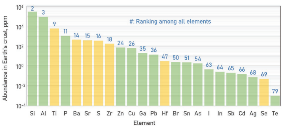
Figure 3. Abundance of elements presented in PV application, with the constituting elements of chalcogenide perovskite emphasized in yellow.
BaZrS3 perovskite is free of heavy metals, which is a good place to start when discussing toxicity. While Ba is poisonous in just a few soluble forms, such as BaCl2, its insoluble molecule, BaSO4, is harmless as well as all other stable compounds. As for sulfur, it is harmless despite taking on specific forms like H2S. Additionally, Zr is constantly present in living organisms. Overall, in terms of elemental abundance and toxicity, BaZrS3 can provide significant advantages over other PV materials.
4.2. Stability
A thermogravimetric study has demonstrated the excellent stability of chalcogenide perovskites, including SrZrS3, BaZrS3, Ba2ZrS4, and Ba3Zr2S7. According to Figure 4.a, the masses of these chalcogenide perovskites remain constant below 600°C, and then dramatically increase from 600°C to 900°C. The XRD and UV-Vis diagrams for BaZrS3 were likewise reported to be undisturbed by long-term atmospheric storage as well as water rinsing.
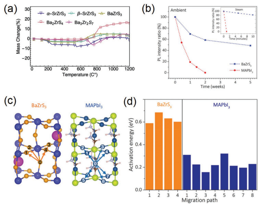
Figure 4. a) Thermogravimetric analysis curves for chalcogenide perovskites. b) Decay curves for photoluminescence intensity from unprotected BaZrS3 comparing to MAPbI3 in ambient environment & steam environment (top right). c) Crystal structures of BaZrS3 and MAPbI3 that demonstrate the anion vacancy migration paths, and d) their activation energies along these paths.
BaZrS3 and MAPbI3 (a typical halide perovskite) were compared in terms of photoluminescence (PL) intensity by Gupta et al. [13]. When exposed to air and water vapor, the PL intensity of MAPbI3 quickly degraded, while BaZrS3 required 5 weeks to reach the same percent of deterioration ratio (Figure 4.b). In the steam test, MAPbI3's photoluminescence entirely stopped after one minute, but the PL intensity of BaZrS3 only decreased by 20% after ten minutes. To be more precise, BaZrS3 has a larger activation energy along all migratory paths than MAPbI3 does (Figure 4.c&d). At room temperature, this difference in activation energy can significantly slow down the vacancy migration rate in BaZrS3. Additionally, because vacancies form and migrate as a result of photo-induced deterioration, the slower rate of vacancy migration in BaZrS3 can significantly alleviate the stability issue with halide perovskites. Since oxidation begins on the surface and spreads into the bulk of perovskites, a reduced diffusion rate of vacancies can typically also slow down the process.
The analysis that follows offers quantitative proof that BaZrS3 is stable. The typical investigation of the BaZrS3 perovskite surfaces is still lacking, though. For the advancement of PV solar cells based on alternative chalcogenide perovskites, as well as the improvement of current halide perovskites, it would be helpful to understand how the surfaces change before and after exposure to air, water vapor, and heat.
4.3. Optoelectronic Properties
In this section, we will talk about the optical absorption and photoluminescence of BaZrS3 and then discuss the nature of its bandgaps like charge transport.
4.3.1. Optical Absorption and Photoluminescence
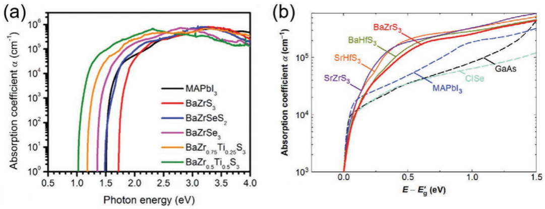
Figure 5. a,b) Absorbance coefficients of several chalcogenide perovskites (calculated and experimentally confirmed independently) with respect to MAPbI3, CuInSe2, and GaAs (measured).
A crucial component of photovoltaic devices is optical absorption. It influences the minimum thickness of the optical absorber layer that is necessary, which in turn regulates the amount of material used. Additionally, a thinner absorption layer can offer charge carriers lower resistance and shorter routes. As a result, higher efficiency and less material usage are associated with improved absorption coefficients. As for BaZrS3, it has an excellent calculated light absorption coefficient (α) which quickly arrived at 105 cm-1 with the photon energy above 2.0eV (Figure 5.a). By comparison with traditional PV materials like MAPbI3, GaAs, and CuInSe2, the absorption coefficient of BaZrS3 has exceeded that of the traditional PV materials by at least one order of magnitude (Figure 5.b). Some experimental data has confirmed the calculation result that α exceeds 2x105 cm-1 at the photon energy of 0.5eV above the bandgap [14]. Therefore, the necessary thickness of the absorber layer is around 500nm for an BaZrS3 high efficiency solar cell, which is less than the thickness of commercialized chalcogenide thin film solar cells.
Effective light emission at open circuit, which is the opposite of light absorption, is a crucial early sign of high PV potential that may be evaluated before the technical difficulties of device integration are faced. Low quasi-Fermi level splitting losses linked to nonradiative recombination are indicated by a high exterior luminescence efficiency (ηext), which in turn suggests a potential for a high open-circuit voltage. However, specific research about the light emission of BaZrS3 is still missing. There is only a related study conducted on SrZrS3 [16]. For SrZrS3 (Eg = 2.13 eV), ηext was 0.05% for one-sun equivalent illumination, which corresponds to 532 nm light and the specified bandgap. Comparing with other inorganic PV materials, SrZrS3 powders already have higher ηext values than top-performing Cu2ZnSn(S,Se)4 solar cells and evaporated CsPbI3 absorber layers [17]. In the same investigation, BaZrS3's photoluminescence intensity was 1/20th that of SrZrS3, but the samples weren't tuned for optoelectronic performance.
These findings give considerable impetus to developing chalcogenide perovskites for photovoltage and photoluminescence applications. In addition, the calculation and experimental data indicate several peculiar characteristics that need further examination.
4.3.2. Bandgap Type and Size. Regarding the size and type of BaZrS3's bandgap, the outcomes of recent investigations are very contradictory. However, they are all in agreement that there is a direct bandgap for BaZrS3. Furthermore, the results from the DFT calculation support this consensus. Consequently, this direct bandgap offers BaZrS3 with an exceptional capacity for light absorption close to the bandgap. In addition, the stated location of the PL peak is quite constant at room temperature [13,14]. Therefore, we may deduce that the bandgap of BaZrS3 is around 1.8eV. And theoretical predictions and practical results both verify that band size discrepancies will not impact the absorption coefficient of BaZrS3.
4.3.3. Charge Carrier Mobility. Few tests on BaZrS3 thin film samples have been undertaken, which is the primary cause of the paucity of knowledge regarding charge transport. Nevertheless, the masses of the holes and electrons are determined by computer predictions. The direction-averaged effective masses for holes and electrons are 0.5m0 and 0.3m0 [12], respectively, whereas the effective masses of electrons and holes in MAPbI3 are 0.2m0 and 0.3m0 [18].
Wei et al. observed that the electron mobility values of the BaZrS3 thin films (n-type) generated by sulfurization of oxide precursors are up to 13.7 cm2 V-1 s-1 [14]. Zeng et al. determined that the hole mobility of an identically generated p-type BaZrS3 thin film was 9.4 cm2 V-1 s-1 [15], whereas other straight bandgap inorganic PV materials, such as CsPbI3 and CZTS, have total mobilities (hole mobility plus electron mobility) between 30 and 40 cm2 V-1 s-1. Due to the varying effects of sample type, quality, measurement technique, and associated uncertainties, further measurements are required for a precise forecast [19].
4.3.4. Defect Chemistry and Doping. Defect chemistry is important for determining if a certain type of material is acceptable for PV usage. As for the creation of deep defects in BaZrS3, theoretical calculation findings are highly encouraging. Moreover, BaZrS3 has a low propensity to develop profound flaws. Under all feasible circumstances, two probable deep defects in BaZrS3, namely ZrS and SZr, need relatively high energy (over 2eV) to develop [12]. Therefore, it would be hard for these two flaws to accumulate in BaZrS3. In comparison, Cu2ZnSnS4 has two possible deep defects, VS and SnZn, both of which have a formation energy < 1eV [20]. In addition, Meng et al. [21] discovered that the S atoms spontaneously reorganize themselves into tiny clusters with S-S bonds, preventing BaZrS3 from deep flaws.
Doping type, doping density, and controllability represent a further crucial part of defect chemistry. Meng et al.'s defect computation identifies a number of probable shallow defects, including Bai, ZrBa, VS, and BaS (donors) and BaZr and VZr (acceptors) [22]. And they found that S-poor growth circumstances are likely to result in degenerate n-type doping by VS, whereas S-rich growth conditions may produce weak p-type material due to the equilibrium of VS and Si.
5. Synthesis and Thin Film Growth of BaZrS3
Even though BaZrS3 chalcogenide perovskite has some similarities with halide perovskites, the synthesis paths are totally different. Here we will first discuss the synthesis of BaZrS3 crystal and then move onto the thin film growth.
5.1. Solid-state BaZrS3 synthesis
As for the synthesis of the BaZrS3 perovskite used in solar cells, several authors reported there is a significant kinetic barrier which blocks the phase formation. For example, under the condition of 900°C, stoichiometrically mixed BaS and ZrS2 do not react. Because a BaZrS3 layer was formed at the interface of the BaS and ZrS2, which blocks the diffusion process of the reacting elements. Therefore, a relative high temperature is required to overcome this diffusion limit.
However, when involving a specific amount of excess molten sulfur (S) phase, everything will be different. Wang et al. successfully synthesized BaZrS3 through solid-sate route at around 500–600°C by applying excess S (α represents the quantity of S excess) [22]. Increasing the value of α, the main products simply follow a pattern: BaS + ZrS2 → BaS2 + ZrS2 → BaZrS3 (+ BaS3) → BaS3 + ZrS3. Therefore it provides a plateau for the fast-formation of BaZrS3.
\( 0.9BaS+0.1{BaCl_{2}}+{ZrS_{2}}+αS→{BaZrS_{3}} (+{S_{2}} {Cl_{2}}) (0.5 \lt α \lt 1.5) \) (1)
This result can be a clear proof that BaZrS3 can be synthesized under an acceptable temperature in PV application. In general, it leads to several important findings: first, a simply formation process of BaZrS3 could be limited by severe kinetic limitations; second, by providing appropriate partial pressure of S, we can synthesis BaZrS3 thin films.
5.2. Thin Film Growth
Before examining the technique of the thin film growth of chalcogenide perovskites, it is necessary to cover the usual approach used for halide perovskites, as it may give some advice and explain why alternative methodologies are required for chalcogenide perovskite BaZrS3.
Direct solution-based deposition is the most common technique for the growth of halide perovskites thin films. For example, for MAPbI3 thin film, we typically prepare a mixed solution with metal halide PbI2, organic cations MA+, and a few additives. Then by applying them onto the surface, the perovskite coating can crystallize after the evaporation of the solvent through gentle heating (250 °C). Due to the fact that halide perovskites are sensitive to air and water vapor, the entire process is conducted in a glove box that is free from outside interference [23].
For the formation of a thin film of BaZrS3, the physical vapor deposition (PVD) technique is the proper option. It could also bring us a purer chalcogenide perovskite thin film than other techniques. As material sources, pure metal elements or their binary sulfides are mixed in advance. Then apply them onto the surface through PVD process. Since pure Sr and Ba elements, as well as their sulfides, are sensitive to air, it is necessary to avoid air exposure. In addition, only after the formation of the ternary phase does the film become totally stable to air and moisture. As discussed in solid-state BaZrS3 synthesis, we hypothesize that introducing a BaS3 intermediate phase that can accelerate the diffusion process. Other types of Ba-rich compositions may also be effective for supplying extra binary phases. In addition, the use of additives to aid the diffusion process may cause low-melting phases, thus affecting the formation of BaZrS3 crystals. However, these techniques have not been used on chalcogenide perovskites thin film growth. And how to get rid of the excess sulfur could also be a problem.
6. Conclusion
Chalcogenide perovskites are a novel material class that eliminates the drawbacks of halide perovskites and other chalcogenide materials. And by thoroughly analyzing the various architectures of tandem solar cells, we can conclude that the optimal open circuit voltage for 2-T and 4-T tandem solar cells that employ c-Si as the bottom sub-cell is between 1.72 and 1.8eV. Within the chalcogenide perovskites, BaZrS3 appears to be the most promising material to fulfill this need.
As for the qualities of BaZrS3, it is composed of naturally occurring components and is non-toxic. In addition, its absorption coefficients surpass those of the majority of halide perovskites and chalcogenides. Existing research focuses mostly on the excellent optoelectronic capabilities of BaZrS3; nevertheless, nearly little is known about the composition of its bandgap. According to theoretical papers, we can only conjecture that BaZrS3 is defect-tolerant at this time.
In contrast to halide perovskites, chalcogenide perovskites, especially BaZrS3, require a higher synthesis temperature for thin film synthesis due to their increased stability. Physical vapor deposition is the most effective technique for growing BaZrS3 thin films. Study of current research disproves that BaZrS3 can only be synthesized at a high temperature, which is incompatible with the conductive substrates typically utilized by tandem solar cells. By examining the production of bulk crystalline BaZrS3, we discovered that there are two factors that inhibit the development of grains. First is the restricted diffusion velocity along the interface of BaS and ZrS2, and second is the use of oxide precursors that make oxygen-sulfur exchange more difficult. Therefore, oxide precursors should be avoided wherever feasible, and the phase formation method of BaS3 can give a quicker kinetic velocity. In addition, an appropriate additive is advised to improve crystallization.
References
[1]. Yoshikawa K, Kawasaki H, Yoshida W, Irie T, Konishi K, Nakano K, Uto T, Adachi D, Kanematsu M, Uzu H, Yamamoto K. Silicon heterojunction solar cell with interdigitated back contacts for a photoconversion efficiency over 26%. Nature energy. 2017 Mar 20;2(5):1-8.
[2]. Shockley W, Queisser HJ. Detailed balance limit of efficiency of p‐n junction solar cells. Journal of applied physics. 1961 Mar;32(3):510-9.
[3]. Cariou R, Benick J, Feldmann F, Höhn O, Hauser H, Beutel P, Razek N, Wimplinger M, Bläsi B, Lackner D, Hermle M. III–V-on-silicon solar cells reaching 33% photoconversion efficiency in two-terminal configuration. Nature Energy. 2018 Apr;3(4):326-33.
[4]. Essig S, Allebé C, Remo T, Geisz JF, Steiner MA, Horowitz K, Barraud L, Ward JS, Schnabel M, Descoeudres A, Young DL. Raising the one-sun conversion efficiency of III–V/Si solar cells to 32.8% for two junctions and 35.9% for three junctions. Nature Energy. 2017 Aug 25;2(9):1-9.
[5]. Minami T. Transparent conducting oxide semiconductors for transparent electrodes. Semiconductor science and technology. 2005 Mar 15;20(4):S35.
[6]. De Vos A. Detailed balance limit of the efficiency of tandem solar cells. Journal of Physics D: Applied Physics. 1980 May 14;13(5):839.
[7]. Dubey A, Adhikari N, Mabrouk S, Wu F, Chen K, Yang S, Qiao Q. A strategic review on processing routes towards highly efficient perovskite solar cells. Journal of Materials Chemistry A. 2018;6(6):2406-31.
[8]. Xie H, Lira-Cantu M. Multi-component engineering to enable long-term operational stability of perovskite solar cells. Journal of Physics: Energy. 2020 Apr 24;2(2):024008.
[9]. M. Fischer, M. Woodhouse, S. Herritsch, J. Trube, International Technology Roadmap for Photovoltaic (ITRPV), VDMA E. V. Photovoltaic Equipment, Frankfurt, Germany 2020.
[10]. Liu J, De Bastiani M, Aydin E, Harrison GT, Gao Y, Pradhan RR, Eswaran MK, Mandal M, Yan W, Seitkhan A, Babics M. Efficient and stable perovskite-silicon tandem solar cells through contact displacement by MgF x. Science. 2022 Jun 23:eabn8910.
[11]. Jain A, Ong SP, Hautier G, Chen W, Richards WD, Dacek S, Cholia S, Gunter D, Skinner D, Ceder G, Persson KA. Commentary: The Materials Project: A materials genome approach to accelerating materials innovation. APL materials. 2013 Jul 18;1(1):011002.
[12]. Meng W, Saparov B, Hong F, Wang J, Mitzi DB, Yan Y. Alloying and defect control within chalcogenide perovskites for optimized photovoltaic application. Chemistry of Materials. 2016 Feb 9;28(3):821-9.
[13]. Gupta T, Ghoshal D, Yoshimura A, Basu S, Chow PK, Lakhnot AS, Pandey J, Warrender JM, Efstathiadis H, Soni A, Osei‐Agyemang E. An Environmentally Stable and Lead‐Free Chalcogenide Perovskite. Advanced Functional Materials. 2020 Jun;30(23):2001387.
[14]. Wei X, Hui H, Zhao C, Deng C, Han M, Yu Z, Sheng A, Roy P, Chen A, Lin J, Watson DF. Realization of BaZrS3 chalcogenide perovskite thin films for optoelectronics. Nano Energy. 2020 Feb 1;68:104317.
[15]. Zeng H. Green, stable and earth abundant ionic PV absorbers based on chalcogenide perovskite. State Univ. of New York (SUNY), Univ. at Buffalo, Buffalo, NY (United States); 2018 May 16.
[16]. Ross RT. Some thermodynamics of photochemical systems. The Journal of Chemical Physics. 1967 Jun 15;46(12):4590-3.
[17]. Cabas‐Vidani A, Haass SG, Andres C, Caballero R, Figi R, Schreiner C, Márquez JA, Hages C, Unold T, Bleiner D, Tiwari AN. High‐Efficiency (LixCu1− x) 2ZnSn (S, Se) 4 Kesterite Solar Cells with Lithium Alloying. Advanced Energy Materials. 2018 Dec;8(34):1801191.
[18]. Giorgi G, Fujisawa JI, Segawa H, Yamashita K. Small photocarrier effective masses featuring ambipolar transport in methylammonium lead iodide perovskite: a density functional analysis. The journal of physical chemistry letters. 2013 Dec 19;4(24):4213-6.
[19]. Herz LM. Charge-carrier mobilities in metal halide perovskites: fundamental mechanisms and limits. ACS Energy Letters. 2017 Jul 14;2(7):1539-48.
[20]. Chen S, Walsh A, Gong XG, Wei SH. Classification of lattice defects in the kesterite Cu2ZnSnS4 and Cu2ZnSnSe4 earth‐abundant solar cell absorbers. Advanced materials. 2013 Mar 20;25(11):1522-39.
[21]. Wu X, Gao W, Chai J, Ming C, Chen M, Zeng H, Zhang P, Zhang S, Sun YY. Defect tolerance in chalcogenide perovskite photovoltaic material BaZrS3. Science China Materials. 2021 Dec;64(12):2976-86.
[22]. Jackson AJ, Tiana D, Walsh A. A universal chemical potential for sulfur vapours. Chemical science. 2016;7(2):1082-92.
[23]. Manser JS, Saidaminov MI, Christians JA, Bakr OM, Kamat PV. Making and breaking of lead halide perovskites. Accounts of chemical research. 2016 Feb 16;49(2):330-8.
Cite this article
Qin,S. (2023). A promising chalcogenide perovskite-BaZrS3-for application on tandem solar cells. Applied and Computational Engineering,7,14-23.
Data availability
The datasets used and/or analyzed during the current study will be available from the authors upon reasonable request.
Disclaimer/Publisher's Note
The statements, opinions and data contained in all publications are solely those of the individual author(s) and contributor(s) and not of EWA Publishing and/or the editor(s). EWA Publishing and/or the editor(s) disclaim responsibility for any injury to people or property resulting from any ideas, methods, instructions or products referred to in the content.
About volume
Volume title: Proceedings of the 3rd International Conference on Materials Chemistry and Environmental Engineering (CONF-MCEE 2023), Part II
© 2024 by the author(s). Licensee EWA Publishing, Oxford, UK. This article is an open access article distributed under the terms and
conditions of the Creative Commons Attribution (CC BY) license. Authors who
publish this series agree to the following terms:
1. Authors retain copyright and grant the series right of first publication with the work simultaneously licensed under a Creative Commons
Attribution License that allows others to share the work with an acknowledgment of the work's authorship and initial publication in this
series.
2. Authors are able to enter into separate, additional contractual arrangements for the non-exclusive distribution of the series's published
version of the work (e.g., post it to an institutional repository or publish it in a book), with an acknowledgment of its initial
publication in this series.
3. Authors are permitted and encouraged to post their work online (e.g., in institutional repositories or on their website) prior to and
during the submission process, as it can lead to productive exchanges, as well as earlier and greater citation of published work (See
Open access policy for details).
References
[1]. Yoshikawa K, Kawasaki H, Yoshida W, Irie T, Konishi K, Nakano K, Uto T, Adachi D, Kanematsu M, Uzu H, Yamamoto K. Silicon heterojunction solar cell with interdigitated back contacts for a photoconversion efficiency over 26%. Nature energy. 2017 Mar 20;2(5):1-8.
[2]. Shockley W, Queisser HJ. Detailed balance limit of efficiency of p‐n junction solar cells. Journal of applied physics. 1961 Mar;32(3):510-9.
[3]. Cariou R, Benick J, Feldmann F, Höhn O, Hauser H, Beutel P, Razek N, Wimplinger M, Bläsi B, Lackner D, Hermle M. III–V-on-silicon solar cells reaching 33% photoconversion efficiency in two-terminal configuration. Nature Energy. 2018 Apr;3(4):326-33.
[4]. Essig S, Allebé C, Remo T, Geisz JF, Steiner MA, Horowitz K, Barraud L, Ward JS, Schnabel M, Descoeudres A, Young DL. Raising the one-sun conversion efficiency of III–V/Si solar cells to 32.8% for two junctions and 35.9% for three junctions. Nature Energy. 2017 Aug 25;2(9):1-9.
[5]. Minami T. Transparent conducting oxide semiconductors for transparent electrodes. Semiconductor science and technology. 2005 Mar 15;20(4):S35.
[6]. De Vos A. Detailed balance limit of the efficiency of tandem solar cells. Journal of Physics D: Applied Physics. 1980 May 14;13(5):839.
[7]. Dubey A, Adhikari N, Mabrouk S, Wu F, Chen K, Yang S, Qiao Q. A strategic review on processing routes towards highly efficient perovskite solar cells. Journal of Materials Chemistry A. 2018;6(6):2406-31.
[8]. Xie H, Lira-Cantu M. Multi-component engineering to enable long-term operational stability of perovskite solar cells. Journal of Physics: Energy. 2020 Apr 24;2(2):024008.
[9]. M. Fischer, M. Woodhouse, S. Herritsch, J. Trube, International Technology Roadmap for Photovoltaic (ITRPV), VDMA E. V. Photovoltaic Equipment, Frankfurt, Germany 2020.
[10]. Liu J, De Bastiani M, Aydin E, Harrison GT, Gao Y, Pradhan RR, Eswaran MK, Mandal M, Yan W, Seitkhan A, Babics M. Efficient and stable perovskite-silicon tandem solar cells through contact displacement by MgF x. Science. 2022 Jun 23:eabn8910.
[11]. Jain A, Ong SP, Hautier G, Chen W, Richards WD, Dacek S, Cholia S, Gunter D, Skinner D, Ceder G, Persson KA. Commentary: The Materials Project: A materials genome approach to accelerating materials innovation. APL materials. 2013 Jul 18;1(1):011002.
[12]. Meng W, Saparov B, Hong F, Wang J, Mitzi DB, Yan Y. Alloying and defect control within chalcogenide perovskites for optimized photovoltaic application. Chemistry of Materials. 2016 Feb 9;28(3):821-9.
[13]. Gupta T, Ghoshal D, Yoshimura A, Basu S, Chow PK, Lakhnot AS, Pandey J, Warrender JM, Efstathiadis H, Soni A, Osei‐Agyemang E. An Environmentally Stable and Lead‐Free Chalcogenide Perovskite. Advanced Functional Materials. 2020 Jun;30(23):2001387.
[14]. Wei X, Hui H, Zhao C, Deng C, Han M, Yu Z, Sheng A, Roy P, Chen A, Lin J, Watson DF. Realization of BaZrS3 chalcogenide perovskite thin films for optoelectronics. Nano Energy. 2020 Feb 1;68:104317.
[15]. Zeng H. Green, stable and earth abundant ionic PV absorbers based on chalcogenide perovskite. State Univ. of New York (SUNY), Univ. at Buffalo, Buffalo, NY (United States); 2018 May 16.
[16]. Ross RT. Some thermodynamics of photochemical systems. The Journal of Chemical Physics. 1967 Jun 15;46(12):4590-3.
[17]. Cabas‐Vidani A, Haass SG, Andres C, Caballero R, Figi R, Schreiner C, Márquez JA, Hages C, Unold T, Bleiner D, Tiwari AN. High‐Efficiency (LixCu1− x) 2ZnSn (S, Se) 4 Kesterite Solar Cells with Lithium Alloying. Advanced Energy Materials. 2018 Dec;8(34):1801191.
[18]. Giorgi G, Fujisawa JI, Segawa H, Yamashita K. Small photocarrier effective masses featuring ambipolar transport in methylammonium lead iodide perovskite: a density functional analysis. The journal of physical chemistry letters. 2013 Dec 19;4(24):4213-6.
[19]. Herz LM. Charge-carrier mobilities in metal halide perovskites: fundamental mechanisms and limits. ACS Energy Letters. 2017 Jul 14;2(7):1539-48.
[20]. Chen S, Walsh A, Gong XG, Wei SH. Classification of lattice defects in the kesterite Cu2ZnSnS4 and Cu2ZnSnSe4 earth‐abundant solar cell absorbers. Advanced materials. 2013 Mar 20;25(11):1522-39.
[21]. Wu X, Gao W, Chai J, Ming C, Chen M, Zeng H, Zhang P, Zhang S, Sun YY. Defect tolerance in chalcogenide perovskite photovoltaic material BaZrS3. Science China Materials. 2021 Dec;64(12):2976-86.
[22]. Jackson AJ, Tiana D, Walsh A. A universal chemical potential for sulfur vapours. Chemical science. 2016;7(2):1082-92.
[23]. Manser JS, Saidaminov MI, Christians JA, Bakr OM, Kamat PV. Making and breaking of lead halide perovskites. Accounts of chemical research. 2016 Feb 16;49(2):330-8.