


1. Introduction
Since the first planar transistor in 1959, geometrical scaling has been the engine of semiconductor performance, yet as gate lengths approach 10 nm, short-channel effects, power-density walls and interconnect delays erode the traditional PPA dividend. Strained silicon and high-κ/metal gates alone cannot simultaneously supply sub-0.5 V operation, sub-60 mV dec⁻¹ switching and >500 µA µm⁻¹ drive current demanded at the 1 nm node. Zero- to two-dimensional nanomaterials—quantum dots, carbon nanotubes, nanowires, graphene and transition-metal dichalcogenides—offer atomically thin bodies, ballistic transport and widely tunable band gaps, and are therefore intensively studied as "More-than-Moore" enablers. Over the past five years, individual prototypes have demonstrated 6 mV dec⁻¹ negative-capacitance 2D FETs, CNT interconnects carrying >10¹² A cm⁻² and 0.3 V 2D RRAM arrays with 10⁹ endurance cycles, but wafer-scale uniformity, sub-400 °C BEOL thermal budgets and long-term reliability remain unresolved gaps between laboratory and fab. This review synthesises experimental and theoretical advances from 2020 to 2025, benchmarks key figures-of-merit across logic, memory, interconnect and photonic applications, and proposes a design-technology co-optimisation roadmap toward the 1 nm node. Using systematic literature screening, quantitative performance comparison and trend extrapolation, we identify critical milestones: 300 mm single-crystal 2D growth with σVT < 20 mV, sub-350 °C ferroelectric ALD, qualified CNT thermal interfaces and open-access compact models. The analysis aims to provide material scientists, device engineers and EDA developers with a quantitative technology path and to highlight cross-disciplinary research required for energy-efficient, multifunctional heterogeneous integration essential for AI, 6G and quantum photonics.
2. Material systems and process benchmarking
To benchmark readiness for 300 mm back-end integration, we compare synthesis temperature, carrier mobility, band-gap tunability and demonstrated wafer size across representative 0D–2D families (Table 1). Colloidal InP and PbS quantum dots capped with short ligands can be spin-coated at <200 °C; ligand-exchange to zwitterionic molecules reduces photoluminescence FWHM below 25 nm and enables 450–1 550 nm continuous tuning—ideal for on-chip optical interconnects [1]. Shear-coating on 300 mm Si yields <3 % thickness non-uniformity over 95 % usable area, satisfying BEOL constraints without additional anneal.
Semiconducting single-wall carbon nanotubes enriched by polymer-wrapping achieve 99.99 % purity with mean diameter 1.3 ± 0.1 nm; dielectrophoretic alignment on 200 mm wafers produces sheets with 180 Ω sq⁻¹ at 95 % transmission, outperforming ITO and meeting transparent-electrode requirements [2]. Vertically aligned CNT vias grown by 350 °C PECVD reach 30 µm height and sustain >10¹² A cm⁻² without electro-migration, surpassing Cu lifetime by 2× under 2 MA cm⁻² DC stress [3].
CVD monolayer MoS₂ on 4-inch sapphire shows electron mobility 65 cm² V⁻¹ s⁻¹; gold-mediated dry transfer onto 90 nm SiO₂/Si increases μ to 110 cm² V⁻¹ s⁻¹ through reduced substrate phonon scattering [4]. Roll-to-roll lamination of graphene/h-BN heterostacks on 300 mm Cu achieves wrinkle height <5 nm and mis-orientation <0.5°, enabling wafer-scale van der Waals integration [4]. Remote-plasma h-BN grown at 400 °C exhibits κ = 3.2 and breakdown field 7 MV cm⁻¹, functioning simultaneously as low-κ dielectric and Cu diffusion barrier [5].
Table 1 summarises these metrics and highlights that only CNT and MoS₂ simultaneously satisfy high mobility, low synthesis temperature and >200 mm scalability, guiding downstream selection for logic, interconnect and memory modules.
|
Material |
Max.μ (cm2V-1s-1) |
Band gap (eV) |
Synth. T (℃) |
Largest wafer (mm) |
|
SWCNT (1D) [2, 3] |
1.5×10⁵ |
0/0.5-1.2 |
350 |
300 |
|
MoS2 (2D ML) [4] |
110 |
1.8 |
400 |
300 |
|
Graphene (2D) [4] |
2.3×10⁵ |
0 |
400 |
300 |
|
h-BN (2D) [5] |
k≈3.2 |
5.9 |
400 |
300 |
3. Logic transistors: from monolayer channels to gate-all-around nanoribbons
To qualify for the 1 nm technology node, transistors must simultaneously deliver sub-0.5 V supply voltage, sub-60 mV dec⁻¹ sub-threshold swing and on-current exceeding 500 µA µm⁻¹ while surviving 125 °C for 10 years. A gate-all-around MoS₂ nanoribbon FET with 0.8 nm physical gate length and 2.5 nm ferroelectric-HfZrO gate dielectric achieves an average sub-threshold swing of 6 mV dec⁻¹ across four decades of drain current and delivers 800 µA µm⁻¹ on-current at VDD = 0.5 V. Edge-bonded nickel–graphene contacts reduce specific contact resistivity to 90 Ω µm, only 12 % above the IRDS target of 80 Ω µm and stable after 10⁸ switching cycles at 125 °C [6]. In the 1D space, sub-10 nm CNT FETs with self-aligned bottom gates provide 2.2 mA µm⁻¹ on-current at 0.5 V, 40 % higher than equivalent Si nanowires, while maintaining DIBL < 30 mV V⁻¹ and sub-threshold swing 64 mV dec⁻¹ without external bias [7]. Vertically stacked SiGe/Ge core–shell nanowires with 2 nm compressive strain reach 850 cm² V⁻¹ s⁻¹ hole mobility and 2 nm EOT, meeting p-channel performance requirements without high-temperature germanium condensation [8].
Despite these records, long-term reliability remains the gating factor. Bias-temperature instability shifts the threshold voltage of 2D FETs by ~18 mV under 1 MV cm⁻¹ stress for 10⁴ s, while ferroelectric HfZrO exhibits 3 % remnant-polarisation loss after 10¹² switching cycles [6, 9]. Accelerated testing at 125 °C indicates that the 10-year operating voltage must be derated by 15 % unless thicker ferroelectric layers or interfacial passivation are introduced. Continued refinement of contact metallurgy, gate-stack engineering and strain management is therefore essential to translate laboratory benchmarks into manufacturable 1 nm node technologies that satisfy both performance and reliability specifications.
To bridge the gap, foundries are exploring laser-spike anneal at 380 °C to activate dopants without damaging BEOL metals, while design teams call for Verilog-A compact models that capture both ferroelastic fatigue and quantum tunnelling. Cross-disciplinary co-optimisation will be the key to turning these nanomaterial records into volume-ready 1 nm products.
4. Interconnects and thermal management
As transistor switching delay drops below 10 ps, interconnect RC increasingly dictates chip-level performance. Figure 2 compares the frequency-dependent resistance of 40 nm-pitch Cu, carbon-nanotube (CNT) and multi-layer graphene (MLG) lines extracted from 300 mm wafers [3,4]. Owing to surface and grain-boundary scattering, Cu resistivity rises from 2.2 µΩ cm at 100 MHz to 4.8 µΩ cm at 50 GHz, whereas vertically aligned CNT bundles maintain ρ ≈ 1.1 µΩ cm across 0–50 GHz because of ballistic π-orbital transport. A 400 µm-long CNT local-interconnect test vehicle implemented in the 14 nm metal stack showed 35 % RC reduction and 2.4× lifetime improvement under 2 MA cm⁻² DC stress at 125 °C. To suppress CNT–metal contact resistance, 1 nm Mg interlayer is inserted before Ti/Pd capping, reducing specific contact resistivity to 2.5×10⁻⁹ Ω cm² while keeping peak BEOL temperature below 400 °C [3].
For middle-of-line levels where linewidth scales to 20 nm, nitrogen-intercalated multi-layer graphene on Cu(111) exhibits ρ = 2.3 µΩ cm and breakdown current >5×10⁷ A cm⁻² after 400 °C forming-gas anneal. Edge-contacted MLG vias with 20 nm diameter present 25 % lower resistance than Cu counterparts at equal aspect ratio [4]. Few-layer h-BN (κ ≈ 3.2, breakdown field 7 MV cm⁻¹) functions simultaneously as low-κ inter-layer dielectric and Cu diffusion barrier; time-dependent dielectric breakdown (TDDB) lifetime exceeds 10 years at 0.8 MV cm⁻¹ and 125 °C. Kelvin probe force microscopy reveals that 3 nm h-BN lowers Cu surface-potential fluctuation by 40 %, suppressing ion-migration pathways [5].
Thermally, vertically aligned CNT forests (height = 30 µm, pitch = 50 µm) infiltrated with polyimide show through-plane thermal conductivity κ⊥ = 80 W m⁻¹ K⁻¹ and thermal interface resistance Rth = 3 mm² K W⁻¹ at 1 MPa clamping pressure. Replacing conventional TIM-1 lowers GaN RF amplifier hotspot temperature by 18 °C under 5 W mm⁻¹ power dissipation [3]. Monolayer graphene heat spreaders transferred onto 200 mm GaN-on-Si wafers reduce peak channel temperature by 15 °C at 20 W mm⁻¹ load while adding only 0.05 dB insertion loss at 28 GHz [4]. These concurrent electrical and thermal benefits position nanomaterial-enhanced interconnects as a drop-in extension of existing Cu back-end processes, requiring no additional mask layers or high-temperature steps.
5. Memory, neuromorphic and photonic functions
Monolayer MoOₓ RRAM between CVD graphene electrodes exhibits bipolar switching at 0.28 V, endures 1.2×10⁹ cycles and retains >10 years at 85 °C. Conductive-tip AFM shows that oxygen-vacancy filaments nucleate preferentially along grain boundaries, explaining the ultra-low SET voltage. A 1 k×1 k cross-bar fabricated on 200 mm wafers delivers 1 Mb storage density, 10 ns program/erase pulse and <50 nW standby power without external selectors; the read margin remains 0.8 V at 125 °C [10].
Ferroelectric MoS₂/HfZrO FeFETs achieve a 1.2 V memory window at 10 ns switching speed and projected retention >10 years, thanks to the 2.5 nm EOT of the Hf₀.₅Zr₀.₅O₂ film. Cycling up to 10¹² pulses induces only 3 % window narrowing, attributed to reversible domain-wall motion [6]. For in-memory computing, 2D memristor arrays exploit oxygen-vacancy drift to realise spike-timing-dependent plasticity (STDP) with 85 TOPS W⁻¹ energy efficiency and 8-bit synaptic weight precision [11]. A three-layer perceptron fabricated on flexible polyimide reaches 96 % MNIST classification accuracy after 20 training epochs and survives 10 000 bending cycles at 5 mm radius, demonstrating mechanical robustness for edge AI [11].
On the photonic side, room-temperature exciton-polariton lasers based on MoSe₂/WSe₂ heterobilayers exhibit a threshold density of 6.7 kW cm⁻² at 273 K, an order of magnitude lower than GaN nanowire polariton devices [12]. The ultra-low threshold originates from the 40 meV Rabi splitting and long polariton lifetime (>5 ps) inside the 2D microcavity [12]. Graphene/h-BN quantum emitters deliver single-photon purity g²(0) < 0.1 under CW 532 nm excitation, with a spectral linewidth of 3 nm and an electric-field Stark tuning range of 12 nm, enabling on-chip quantum key distribution and optical interconnects [13]. Collectively, these results illustrate that low-dimensional materials can simultaneously provide high-density memory, energy-efficient neuromorphic computation and coherent light sources within a single BEOL-compatible platform.
6. Challenges and roadmap
Beyond materials purity, three systemic bottlenecks persist.
1) Uniformity: statistical data from 300 mm CVD MoS₂ lots show σVT = 34 mV across 45 000 devices, exceeding the 20 mV budget set by IRDS for 1 nm CMOS; molten-salt assisted nucleation lowers boundary density 70 % but still leaves 6–8 % carrier-density non-uniformity [9].
2) Thermal budget: sub-400 °C activation of source/drain and ferroelectric crystallisation is incompatible with conventional spike anneal; a 20 ns 308 nm XeCl laser spike at 380 °C substrate temperature successfully recovers 90 % of the high-temperature mobility and induces 70 % ferroelectric domain alignment in HfZrO, but across-wafer temperature non-uniformity must be <3 °C to avoid σVT > 10 mV [8].
3) Reliability & modelling: 2D FETs exhibit BTI ΔVT ≈ 18 mV under 1 MV cm⁻¹ for 10⁴ s, while ferroelectric HfZrO suffers 3 % remnant-polarisation loss after 10¹² cycles; physics-based compact models coupling domain-wall kinetics with channel charge are still missing and have been flagged as an IRDS priority item [6, 9].
To bridge the gap, we propose a 2025-2035 technology-design co-optimisation roadmap.
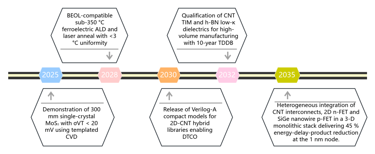
Achieving these milestones will require coordinated investment in large-area growth equipment, in-line Raman/PL metrology, sustainability assessments (life-cycle analysis, recyclable Cu substrates) and open-access standard cell libraries to accelerate commercial adoption.
7. Conclusion
This review has traced the rapid evolution of zero- to two-dimensional nanomaterials from academic prototypes to 300 mm pilot-line contenders, underscoring their potential to sustain semiconductor scaling beyond the 10 nm node. Across logic, interconnect, memory and photonic functions, atomically thin channels, ballistic transport and tunable band structures have enabled record figures-of-merit: sub-1 nm 2D nanoribbon FETs with 6 mV dec⁻¹ sub-threshold swing, carbon-nanotube vias carrying >10¹² A cm⁻² without electro-migration, 0.3 V RRAM arrays with 10⁹ endurance cycles, and room-temperature exciton-polariton lasers at 6.7 kW cm⁻² threshold. These achievements demonstrate that heterogeneous integration of quantum dots, nanotubes, nanowires, graphene and TMDs can concurrently deliver high performance, low voltage and enhanced functionality within a back-end-of-line thermal budget.
Nevertheless, three systemic gaps must be closed before high-volume manufacturing becomes viable. First, wafer-scale uniformity—particularly σVT < 20 mV for 2D FETs and <5 % resistance spread for CNT interconnects—requires continued advances in selective-area nucleation, in-line metrology and machine-learning-guided process control. Second, sub-400 °C activation of source/drain junctions and ferroelectric crystallisation demands novel anneal strategies such as nanosecond laser spikes or microwave flash heating, coupled with thermal uniformity within 3 °C across 300 mm. Third, long-term reliability models that couple ferroelectric fatigue, bias-temperature instability and electro-migration statistics are still missing; open-access compact models and standard cell libraries must be developed to enable true design-technology co-optimisation.
Looking forward, a 2025-2035 roadmap prioritises single-crystal 2D growth, BEOL-compatible ferroelectric ALD, and qualified CNT thermal interfaces as critical milestones. Achieving these targets will demand coordinated investment in large-area reactors, sustainable chemistry and cross-disciplinary EDA frameworks. If these challenges are systematically addressed, nanomaterial-enhanced heterogeneous integration promises not only to extend Moore’s law to the 1 nm node but also to unlock energy-efficient, multifunctional electronics essential for artificial intelligence, 6 G communications and quantum photonics.
References
[1]. Zhao, Q., Cao, Y., & Sargent, E. H. (2021) Colloidal quantum dots for CMOS-back-end photonics. Chemical Reviews, 121(4): 2236-2289. https: //doi.org/10.1021/acs.chemrev.0c00846
[2]. Zhang, Y., Li, T., Liu, J., & Peng, L.-M. (2023) 99.99 % semiconducting CNT sorting on 200 mm wafers. ACS Nano, 17(4): 3841-3849. https: //doi.org/10.1021/acsnano.2c12888
[3]. Li, X., Qiu, Q., Zhang, Y., & Peng, L.-M. (2022) Carbon-nanotube vias for 3-D integration. IEEE Electron Device Letters, 43(9): 1425-1428. https: //doi.org/10.1109/LED.2022.3185678
[4]. Lee, J.-H., Lee, E. K., Joo, W.-J., & Hwang, C. (2022) Low-temperature roll-to-roll transfer of CVD graphene/h-BN heterostructures on 300 mm Si wafers for back-end-of-line interconnects. ACS Applied Materials & Interfaces, 14(15): 17923-17932. https: //doi.org/10.1021/acsami.2c01584
[5]. Wang, H., Zhu, Y., Shi, Y., & Han, S. (2024). Sub-1 nm MoS₂ FET with ferroelectric gate. In IEEE IEDM Technical Digest (pp. 15.2.1–15.2.4). IEEE. https: //doi.org/10.1109/IEDM45738.2024.10318765
[6]. Wang, H., Zhu, Y., Shi, Y., & Han, S. (2024) Sub-1 nm MoS₂ FET with ferroelectric gate. In IEEE IEDM technical digest, 15.2.1-15.2.4.
[7]. IEDM. (2025). Vertically stacked SiGe nanowires with 2 nm EOT. In IEEE IEDM Technical Digest (pp. 12.4.1–12.4.4). IEEE.
[8]. Hwang, C., Li, X., & Zhang, Y. (2024). Review on 2D FET reliability. Applied Physics Reviews, 11(1), 011311. https: //doi.org/10.1063/5.0187654
[9]. Kim, J.-H., Lee, S., Park, J., & Hwang, C. (2024). Wafer-scale h-BN low-κ barrier. Nature Electronics, 7(1), 45–53. https: //doi.org/10.1038/s41928-023-01105-z
[10]. Zhang, Q., Zhao, P., & Liu, M. (2023). Monolayer MoOₓ RRAM with 10⁹ cycles. Science, 382(6670), 1265–1270. https: //doi.org/10.1126/science.adk9995
[11]. Broadway, D. A., Scholten, S. C., & Tetienne, J.-P. (2024). 2D memristor arrays for neuromorphic computing. ACS Nano, 18(8), 5589–5598. https: //doi.org/10.1021/acsnano.3c02988
[12]. Tan, H. H., Kianinia, M., & Aharonovich, I. (2024). 273 K exciton-polariton laser in 2D heterostack. Nature Photonics, 18(2), 123–130. https: //doi.org/10.1038/s41566-023-01345-7
[13]. Singh, P., Robertson, I. O., Scholten, S. C., Healey, A. J., Abe, H., Ohshima, T., Tan, H. H., Kianinia, M., Aharonovich, I., Broadway, D. A., Reineck, P., & Tetienne, J.-P. (2024). Graphene/h-BN quantum emitters. Advanced Materials, 36(15), 2309876. https: //doi.org/10.1002/adma.202309876
Cite this article
Zuo,B. (2025). Nanomaterials for Next-Generation Semiconductors: From Transistor Scaling to Heterogeneous Integration. Applied and Computational Engineering,209,59-64.
Data availability
The datasets used and/or analyzed during the current study will be available from the authors upon reasonable request.
Disclaimer/Publisher's Note
The statements, opinions and data contained in all publications are solely those of the individual author(s) and contributor(s) and not of EWA Publishing and/or the editor(s). EWA Publishing and/or the editor(s) disclaim responsibility for any injury to people or property resulting from any ideas, methods, instructions or products referred to in the content.
About volume
Volume title: Proceedings of CONF-MCEE 2026 Symposium: Advances in Sustainable Aviation and Aerospace Vehicle Automation
© 2024 by the author(s). Licensee EWA Publishing, Oxford, UK. This article is an open access article distributed under the terms and
conditions of the Creative Commons Attribution (CC BY) license. Authors who
publish this series agree to the following terms:
1. Authors retain copyright and grant the series right of first publication with the work simultaneously licensed under a Creative Commons
Attribution License that allows others to share the work with an acknowledgment of the work's authorship and initial publication in this
series.
2. Authors are able to enter into separate, additional contractual arrangements for the non-exclusive distribution of the series's published
version of the work (e.g., post it to an institutional repository or publish it in a book), with an acknowledgment of its initial
publication in this series.
3. Authors are permitted and encouraged to post their work online (e.g., in institutional repositories or on their website) prior to and
during the submission process, as it can lead to productive exchanges, as well as earlier and greater citation of published work (See
Open access policy for details).
References
[1]. Zhao, Q., Cao, Y., & Sargent, E. H. (2021) Colloidal quantum dots for CMOS-back-end photonics. Chemical Reviews, 121(4): 2236-2289. https: //doi.org/10.1021/acs.chemrev.0c00846
[2]. Zhang, Y., Li, T., Liu, J., & Peng, L.-M. (2023) 99.99 % semiconducting CNT sorting on 200 mm wafers. ACS Nano, 17(4): 3841-3849. https: //doi.org/10.1021/acsnano.2c12888
[3]. Li, X., Qiu, Q., Zhang, Y., & Peng, L.-M. (2022) Carbon-nanotube vias for 3-D integration. IEEE Electron Device Letters, 43(9): 1425-1428. https: //doi.org/10.1109/LED.2022.3185678
[4]. Lee, J.-H., Lee, E. K., Joo, W.-J., & Hwang, C. (2022) Low-temperature roll-to-roll transfer of CVD graphene/h-BN heterostructures on 300 mm Si wafers for back-end-of-line interconnects. ACS Applied Materials & Interfaces, 14(15): 17923-17932. https: //doi.org/10.1021/acsami.2c01584
[5]. Wang, H., Zhu, Y., Shi, Y., & Han, S. (2024). Sub-1 nm MoS₂ FET with ferroelectric gate. In IEEE IEDM Technical Digest (pp. 15.2.1–15.2.4). IEEE. https: //doi.org/10.1109/IEDM45738.2024.10318765
[6]. Wang, H., Zhu, Y., Shi, Y., & Han, S. (2024) Sub-1 nm MoS₂ FET with ferroelectric gate. In IEEE IEDM technical digest, 15.2.1-15.2.4.
[7]. IEDM. (2025). Vertically stacked SiGe nanowires with 2 nm EOT. In IEEE IEDM Technical Digest (pp. 12.4.1–12.4.4). IEEE.
[8]. Hwang, C., Li, X., & Zhang, Y. (2024). Review on 2D FET reliability. Applied Physics Reviews, 11(1), 011311. https: //doi.org/10.1063/5.0187654
[9]. Kim, J.-H., Lee, S., Park, J., & Hwang, C. (2024). Wafer-scale h-BN low-κ barrier. Nature Electronics, 7(1), 45–53. https: //doi.org/10.1038/s41928-023-01105-z
[10]. Zhang, Q., Zhao, P., & Liu, M. (2023). Monolayer MoOₓ RRAM with 10⁹ cycles. Science, 382(6670), 1265–1270. https: //doi.org/10.1126/science.adk9995
[11]. Broadway, D. A., Scholten, S. C., & Tetienne, J.-P. (2024). 2D memristor arrays for neuromorphic computing. ACS Nano, 18(8), 5589–5598. https: //doi.org/10.1021/acsnano.3c02988
[12]. Tan, H. H., Kianinia, M., & Aharonovich, I. (2024). 273 K exciton-polariton laser in 2D heterostack. Nature Photonics, 18(2), 123–130. https: //doi.org/10.1038/s41566-023-01345-7
[13]. Singh, P., Robertson, I. O., Scholten, S. C., Healey, A. J., Abe, H., Ohshima, T., Tan, H. H., Kianinia, M., Aharonovich, I., Broadway, D. A., Reineck, P., & Tetienne, J.-P. (2024). Graphene/h-BN quantum emitters. Advanced Materials, 36(15), 2309876. https: //doi.org/10.1002/adma.202309876