


1. Introduction
A digital clock is a timing device that displays the "hour", "minute", and "second" on the human visual organ. Its timing cycle is 24 hours, and its full-scale display is 23:59:59 seconds. A basic digital clock circuit mainly consists of a second signal generator, an "hour, minute, second," counter, a decoder, and a display. Due to the use of pure digital hardware design and production, compared with traditional mechanical watches, it has the characteristics of accurate travel time, intuitive display, and no mechanical transmission device. The digital clock in this design uses digital circuits to display and adjust "time", "minute", and "second". By using various integrated digital chips to build circuits to achieve corresponding functions. Specifically, counters, decoders, and NAND, XOR gate integrated chips are used. This circuit has the function of timing. After analysing the entire module and drawing the overall circuit diagram, simulate each module and record the results observed during the simulation. Experiments show that the designed circuit can basically meet the design requirements.
2. General overview of main design scheme
The digital electronic clock is composed of several digital integrated circuits, including six parts: timing circuit, counter, numerical comparator, alarm clock, decoder and display. The standard second signal generator is composed of an oscillator and a frequency divider, that is, it generates a pulse signal of 1 Hz, the signal input system, the counters of different scales generate counts, the decoder and display, the time calibration circuit can calibrate the time and minute, the alarm clock circuit and the hour alarm circuit can give the time prompt at the set time and hour time, and the digital electronic clock consists of the following parts: second pulse generator, correction circuit 60 base second, minute counter and 24 base time counter as well as the decoding display part of second, minute and hour [1]. The overall design block diagram is shown below in Figure 1.
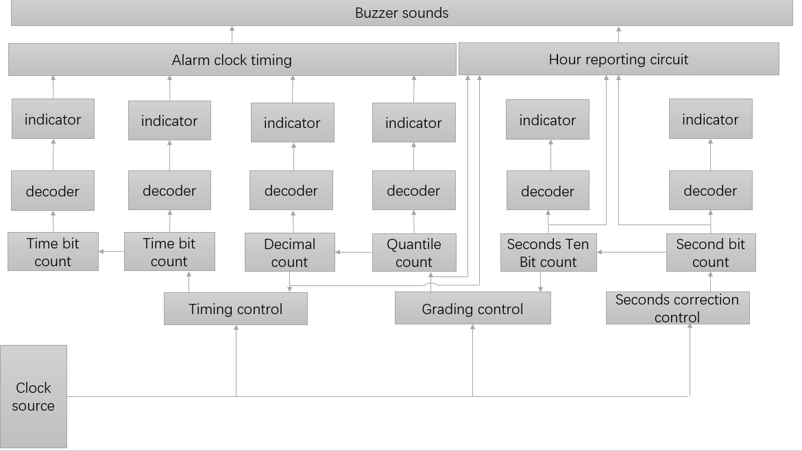
Figure 1. Basic principle logic block diagram.
It can be seen from the above figure that the signal generated by the oscillator passes through the frequency divider as a second pulse, and the second pulse is sent to the counter. The counting result passes through "hour", "minute" and "second", and the decoder displays the time. The oscillator and frequency divider constitute the standard second pulse signal generator, and the timing system is composed of counters, decoders and display circuits of different scales. The second signal is sent to the counter for counting, and the accumulated results are displayed in "hour", "minute" and "second". The "hour" display consists of a decimal counter, a decoder and a display; The display of "minute" and "second" is composed of 60 decimal counters, decoder and display respectively; The timing circuit realizes the calibration of time and minute [2].
3. Main body of digital alarm clock
3.1. Power supply part
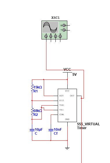
Second generation circuit - oscillator is the core of the timer. The stability and frequency accuracy of the oscillator determine the accuracy of the timer. Generally speaking, the higher the frequency of the oscillator, the higher the timing accuracy, but the greater the power consumption. To form a digital clock, you should first select a pulse source that can automatically generate a stable standard time pulse signal. The pulse signal generated by the pulse source has a higher frequency, namely "second pulse signal" (frequency is 1HZ). Send the standard second signal to the "second counter". The "second counter" uses a 60-base counter, and sends a "minute pulse" signal every 60 seconds, which will be used as the clock pulse of the "minute counter". The "minute counter" also uses the 60-base counter. Every 60 minutes accumulated, a "time pulse" signal is sent, and the signal will be sent to the "time counter". The "hour counter" adopts a 24-base timer, which can accumulate 24 hours a day. At this time, it is necessary to design 60 and 24 base counters respectively. The output signals of each counter are sent to the digital display through the decoder, so that the "hour", "minute" and "second" can be displayed digitally.
The circuit that generates the second signal has many forms. Now the 555 timer is used to form the second signal generator, as shown in the figure below. R1, R2 and C are external timing elements. Connect the high-level trigger THR of 555 timers with the low-level trigger TRI, connect the connection of R2 and C, connect the discharge terminal DIS to the connection of R1 and R2, and connect the CON terminal with a 10nf filter capacitor to improve the stability of the circuit, or not [3]. As can be seen in Figure 2.
| Figure 2. Power supply part. |
3.2. Minute and second circuit parts
The counter is used in the counting circuit, and the counter can be divided into synchronous and asynchronous. Here, the counting circuit uses a 24-base counter. The Minute and second circuit parts can be seen in Figure 3.
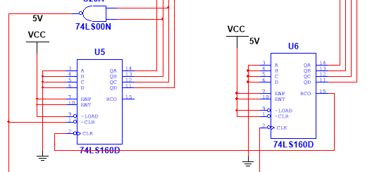
Figure 3. Minute and second circuit parts.
The 74160 counter not only has the function of binary addition counting, but also has additional functions such as preset number, hold, and asynchronous zero setting. In the figure, LD is the preset numerical control terminal, A-D is the data input terminal, CLK is the carry output terminal, CLR is the asynchronous zero setting terminal, and ENP and ENT are the working state control terminals [4].
With the "second" signal, the counters of "second", "minute" and "hour" can be selected according to the system of 60 seconds as 1 minute, 60 minutes as 1 hour, and 24 hours as 1 day. In the "second" counter, only 60 "second" signals can output a "minute" carry signal because it is in 60 decimals. If a decimal number is used to represent a number that requires two decimal digits (one digit and ten digits), then the "second" should be decimal, and the "second" should be hexadecimal, which is in line with people's habit of counting. The "second" counter is usually composed of the integrated chip of two decimal counters, and then the feedback reset method is used to make the "second" ten bits turn into hexadecimal, so as to make the single bits and ten bits combine to realize the 60 decimals.
The number of bits is decimal. The synchronous cascade mode is adopted between the one-bit and ten-bit counters. The carry output signal of the one-bit counter is connected to the ten-bit counter CLK to complete the carry control of the one-bit to ten-bit counter. Select the 10-bit counter QC and QB as the feedback end, and output the control CLR through the NAND gate, which is connected to the hexadecimal count form [5]. When the counter status is 60, it will instantly and asynchronously reset 00000000 and output a carry.
3.3. 24-hour circuit part
The 24-base time counter is also connected by two 74ls160 chips. Its low bit is also a decimal counter, and the signal terminal is the carry signal of the sub-unit. The high-order pulse signal is the carry signal of the low-order time unit [6]. When the high count is 0001 and the low count is 0010, the two 74ls160 counts of the time unit are cleared to 00 by CLR zeroing terminal control when the real-time counter counts to 24, thus forming a 24-base time counter.
3.4. Decoding circuit part
74LS48 is an integrated circuit chip, which is a commonly used seven-segment decoder. It can convert binary digits into corresponding digits on seven-segment LED digital displays, so it is often used in applications such as digital displays and counters.74LS48 has four input ports A, B, C, D, these input ports through the binary code to control the output of seven LED display. 74LS48 can recognize numbers 0-9, as well as some letters and symbols [7].
In addition to the four input ports A, B, C, and D, 74LS48 has two Enable ports, namely LE (Latch Enable) and LT (Lamp Test). LE port is used to control the working mode of 74LS48. When LE=0, 74LS48 is in the latched state, and when LE=1, 74LS48 is in the normal decoding state. The LT port is used to test whether each segment of the seven-segment LED digital display is working properly.
In the output port, 74LS48 has 7 segment select ports, corresponding to the seven segments of LED digital display a, b, c, d, e, f, g segment. In addition, the 74LS48 also has a DP (decimal point) port, which is used to control the switching of the decimal point [8]. The 74ls48 decoding output style is shown in Figure 4.
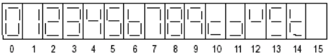
Figure 4. 74ls48 decoding output style.
The function of the decoding circuit is to translate the output code of the "second", "minute" and "hour" counters into corresponding numbers. The decoder used to drive the LED seven-segment digital tube is usually 74LS48. If each output of the "second", "minute" and "hour" counters is connected to the input of the corresponding seven-segment decoder respectively, and then connected to the corresponding digital tube pin after 74ls48 coding, different numbers can be displayed shown in Figure 5.
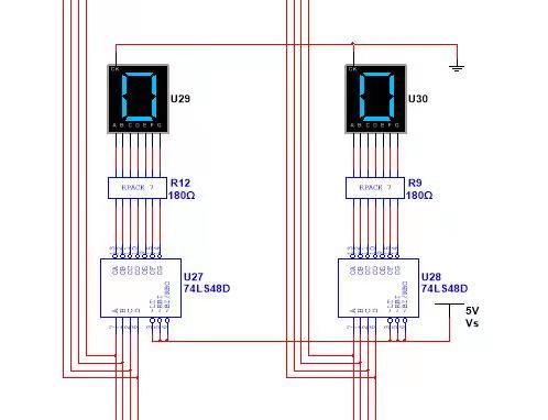
Figure 5. Decoding circuit part.
3.5. Timing circuit part
In this design, the digital clock is calibrated by a single-pole double-throw switch. One end of the switch is 555 signal sources, and the other end is connected to the low signal end of the sub-unit and the time unit respectively [9]. The signal is connected to 555 through a single-pole double-throw switch, and the generated pulse is used to calibrate the time and sub-unit respectively [10].
4. Additional features
4.1. Hour reporting design
The time reporting circuit is the circuit that generates the time reporting signal at the time of the hour. The minute and the second of the hour are both zero, and the binary code is the zero-zero circuit. It mainly uses the four-input or not gate to connect to the tens and tens of the minute circuit and the tens and tens of the second circuit respectively. The output terminal 0000 passes through the or not gate and outputs the high level, and the output result after the tens and tens pass through the or not gate is output through the AND gate. The principle of the second hour detection circuit is the same. When the two outputs the result, the high level is output through the and gate, which triggers the buzzer to work. This is the principle of the hour alarm circuit shown in Figure 6.
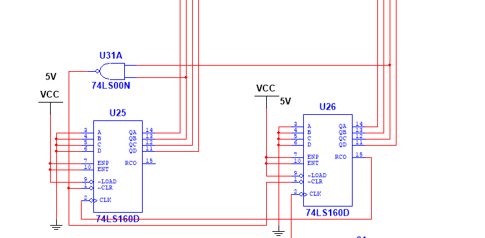
Figure 6. Hour reporting design.
4.2. Alarm clock design
After the 8-bit value input part is powered on, the high level (5V) is the corresponding logic input 1; Low level (grounded, 0V) corresponds to logic input 0. The status conversion between logic 0 and logic 1 is realized by the dial switch. It is worth noting that the 4585 digital comparator works normally under the following conditions: the input AGTB, ALTB is connected to the logic low level, and AEQB is connected to the logic high level. The Figure 7 below shows an 8-bit numerical comparator formed by two 4585 numerical comparators in series.
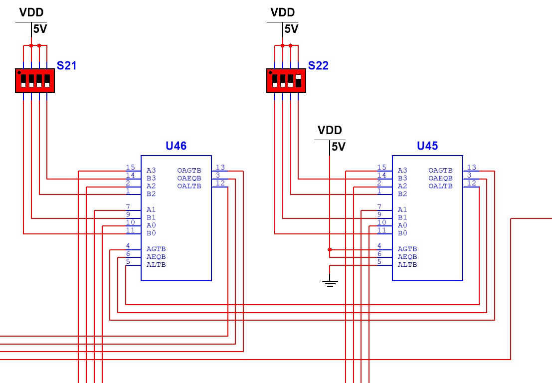
Figure 7. Alarm clock design.
For these two 8 digits, if the upper 4 digits are the same, their size is determined by the comparison results of the lower 4 digits. Therefore, the comparison result of the lower 4 bits should be used as the condition of the higher 4 bits (the higher 4 bits are compared again), that is, the input terminals of the lower 4 bits comparator, OAGTB, OAEQB, and OALTB, should be connected with the AGTB, AEQB, and ALTB terminals of the higher 4 bits comparator respectively. Through expansion, the output in U2 is the high 4-bit input, and the output in U1 is the low 4-bit input. If the output terminal in U2 is a>b, the output OAGTB is high level, the rest is low level, and the red light is on; If a=b, the output OAEQB is high level, the rest is low level, and the red light is on. If a<b, the output OALTB is high, and the rest is low.
5. Conclusion
The design of the electronic alarm clock in this paper is composed of the second pulse circuit module, the counting circuit module, the decoding and display circuit module, and the timing circuit module, with the addition of the clock and alarm clock functions. Through the design, manufacture and simulation of the digital electronic clock, we can improve our proficiency in using the multimedia software and understanding of the digital circuit, which is an opportunity to combine knowledge and practice, it will be of great help for us to learn advanced circuits and practical design in the future.
References
[1]. W. J. Xu and T. Wu, “Design of Temperature Detection Alarm Circuit Based on Multisim,” Applied Mechanics and Materials, vol. 457–458, pp. 1627–1630, Oct. 2013.
[2]. X. Feng, “A Design of LED Digital Tube Intelligent Alarm Clock Based on MCU,” Proceedings of the 2017 International Conference on Information Technology and Intelligent Manufacturing (ITIM 2017), 2017.
[3]. J. Huang, “Design of Electronic Clock based on STM32,” IOP Conference Series: Materials Science and Engineering, vol. 242, p. 012126, Sep. 2017.
[4]. H. Li and J. Yang, “Design of fire alarm system of intelligent camera based on fuzzy recognition algorithm,” Journal of Intelligent & Fuzzy Systems, pp. 1–13, Feb. 2021.
[5]. J. Albert and M. Rooman, “Design Principles of a Genetic Alarm Clock,” PLoS ONE, vol. 7, no. 11, p. e47256, Nov. 2012.
[6]. E. Zhang, “Installation and maintenance for fire alarm systems,” Elderly Care, vol. 6, no. 6, pp. 41–41, Nov. 2019.
[7]. Ghosh, D., et al. “A Novel Design of Seven Segment Decoder Using Cyclic Combinational Technique.” Journal of Low Power Electronics, vol. 9, no. 4, Dec. 2013, pp. 421–26.
[8]. Yang, Yi Hui, and Feng Yuan. “Attendance Machine for Teaching.” Applied Mechanics and Materials, vol. 536-537, Apr. 2014, pp. 1746–50.
[9]. M. Zhong, “Solar Tracking System Using Pic16f84a, Stepper Motor and 555 Timer.” International Journal of Latest Trends in Engineering and Technology, vol. 9, no. 2, 2017.
[10]. Sadeghi, Ayoub, et al. “An Efficient Counter-Based Wallace-Tree Multiplier with a Hybrid Full Adder Core for Image Blending.” Frontiers of Information Technology & Electronic Engineering, vol. 23, no. 6, June 2022, pp. 950–65.
Cite this article
Cheng,L. (2023). Digital and analysis of alarm clock design based on Multisim. Applied and Computational Engineering,9,288-294.
Data availability
The datasets used and/or analyzed during the current study will be available from the authors upon reasonable request.
Disclaimer/Publisher's Note
The statements, opinions and data contained in all publications are solely those of the individual author(s) and contributor(s) and not of EWA Publishing and/or the editor(s). EWA Publishing and/or the editor(s) disclaim responsibility for any injury to people or property resulting from any ideas, methods, instructions or products referred to in the content.
About volume
Volume title: Proceedings of the 2023 International Conference on Mechatronics and Smart Systems
© 2024 by the author(s). Licensee EWA Publishing, Oxford, UK. This article is an open access article distributed under the terms and
conditions of the Creative Commons Attribution (CC BY) license. Authors who
publish this series agree to the following terms:
1. Authors retain copyright and grant the series right of first publication with the work simultaneously licensed under a Creative Commons
Attribution License that allows others to share the work with an acknowledgment of the work's authorship and initial publication in this
series.
2. Authors are able to enter into separate, additional contractual arrangements for the non-exclusive distribution of the series's published
version of the work (e.g., post it to an institutional repository or publish it in a book), with an acknowledgment of its initial
publication in this series.
3. Authors are permitted and encouraged to post their work online (e.g., in institutional repositories or on their website) prior to and
during the submission process, as it can lead to productive exchanges, as well as earlier and greater citation of published work (See
Open access policy for details).
References
[1]. W. J. Xu and T. Wu, “Design of Temperature Detection Alarm Circuit Based on Multisim,” Applied Mechanics and Materials, vol. 457–458, pp. 1627–1630, Oct. 2013.
[2]. X. Feng, “A Design of LED Digital Tube Intelligent Alarm Clock Based on MCU,” Proceedings of the 2017 International Conference on Information Technology and Intelligent Manufacturing (ITIM 2017), 2017.
[3]. J. Huang, “Design of Electronic Clock based on STM32,” IOP Conference Series: Materials Science and Engineering, vol. 242, p. 012126, Sep. 2017.
[4]. H. Li and J. Yang, “Design of fire alarm system of intelligent camera based on fuzzy recognition algorithm,” Journal of Intelligent & Fuzzy Systems, pp. 1–13, Feb. 2021.
[5]. J. Albert and M. Rooman, “Design Principles of a Genetic Alarm Clock,” PLoS ONE, vol. 7, no. 11, p. e47256, Nov. 2012.
[6]. E. Zhang, “Installation and maintenance for fire alarm systems,” Elderly Care, vol. 6, no. 6, pp. 41–41, Nov. 2019.
[7]. Ghosh, D., et al. “A Novel Design of Seven Segment Decoder Using Cyclic Combinational Technique.” Journal of Low Power Electronics, vol. 9, no. 4, Dec. 2013, pp. 421–26.
[8]. Yang, Yi Hui, and Feng Yuan. “Attendance Machine for Teaching.” Applied Mechanics and Materials, vol. 536-537, Apr. 2014, pp. 1746–50.
[9]. M. Zhong, “Solar Tracking System Using Pic16f84a, Stepper Motor and 555 Timer.” International Journal of Latest Trends in Engineering and Technology, vol. 9, no. 2, 2017.
[10]. Sadeghi, Ayoub, et al. “An Efficient Counter-Based Wallace-Tree Multiplier with a Hybrid Full Adder Core for Image Blending.” Frontiers of Information Technology & Electronic Engineering, vol. 23, no. 6, June 2022, pp. 950–65.