


1. Introduction
With the development of modern automobile technology and industry, the exploitation of oil resources on the earth has reduced oil resources year by year. As a result, there is a growing awareness of the need to reduce the use of oil and turn to use renewable resources. Then the electric car was born. In the charging process of electric vehicles (EVs), efficiency is a very important index and a very important factor affecting efficiency is the power factor. The Power factor is equal to the ratio of active power to apparent power. Apparent power is the amount of AC equipment capacity; active power refers to the actual output or consumption of AC power per unit of time. Active power and reactive power are generated when electrical equipment is working. The work in [1] describes the concept of harmonics and power factors. The THD is one of the important factors affecting the power factor. The smaller the THD, the greater the power factor, which means that the electrical equipment used is efficient and has good performance.
The work in [2] introduces a variety of charging modes of electric vehicles to readers, among which the charging mode requiring PFC is a high-power charging pile. According to [2], the capacity of a high-power charging pile is 1000V and the current is 350A. If the battery allows, the car can be charged with 350A high current, greatly reducing the charging time. If the voltage that the car battery can withstand is higher or lower than the charging pile voltage, the adjustable voltage power factor correction (PFC) solves this problem perfectly, and the charging efficiency is extremely high.
The charging process of EVs can use a two-level or three-level structure. The two-level structure shown in [3] is the pre-stage AC-DC PFC and the post-stage DC-DC structure respectively. A brief block diagram is shown in Figure 1. The two-level structure. The advantage of this two-level structure is that the harmonic component of the former AC-DC PFC structure is greatly reduced after the AC is converted to DC, and the harmonic interference to the latter DC-DC part is reduced. In addition, most of the current PFC topologies are adjustable voltages, which can be applied to any scenario where the input voltage is different from the preset battery voltage. This paper focuses on the introduction of a variety of different topologies of single-phase PFC, component composition, working principle, analysis of the working characteristics of each topology, and makes a comparison and conclusion. They are summarized in two parts: fundamental topologies and modified topologies.

Figure 1. The two-level structure.
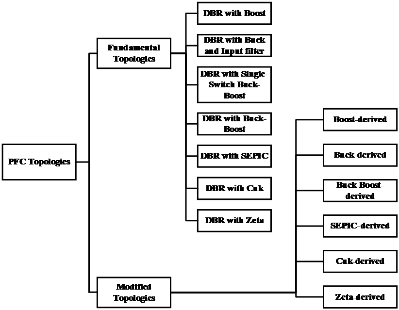
Figure 2. The classification of PFC topologies.
As shown in Figure 2. The classification of PFC topologies, and topologies of single-phase Non-Isolated PFC can be divided into two main categories. The first type is 7 fundamental topologies, all of which are diode bridge rectifier (DBR) and boost circuits; buck with input filter circuits; single-switch buck-boost circuits; buck-boost circuits; SEPIC circuit; Cuk circuits, and Zeta circuit composite. The second type is 6 kinds of modified topology: boost circuit, buck circuit, buck-boost circuit, SEPIC circuit, Cuk circuit, and Zeta circuit modified circuit respectively.
Now, this article will give a brief overview of the branches of each of the seven improved derived circuits. Boost-derived circuits consist of the following topologies: bridgeless boost topology, interleaved boost topology, bridgeless dual boost topology, bridgeless interleaved topology and Semi-bridgeless boost topology. Buck-derived circuits include four kinds of bridgeless topology, DBR with Interleaved Buck topology and bridgeless Interleaved topology. Buck-Boost derived circuit also includes four bridgeless topologies, bridgeless cascaded buck-boost topology, DBR with Interleaved cascaded buck-boost topology, and DBR with Two-switch buck-boost topology. SEPIC-derived circuits include 6 bridgeless topologies and a DBR with Interleaved SEPIC topology. Cuk-derived circuits contain four bridgeless topologies, the bridgeless Inductor switched Cuk topology and one DBR with Inductor Switched Cuk topology. Zeta-derived circuits include 2 bridgeless topologies and a DBR Interleaved Zeta topology.
This paper will show the circuit structure of the first type of classification: seven fundamental topologies to the reader, and analyze the working principle, working characteristics, and the advantages and disadvantages of each topology. There are more than a dozen types of improved topologies extended from the fundamental topologies. This paper will not introduce any of them, but mainly introduce the bridgeless improved topologies among them.
2. Fundamental topologies
2.1. DBR with boost topology

Figure 3. DBR with Boost topology.
The Boost circuit is one of the six chopper circuits, a switching DC booster circuit that makes the output voltage higher than the input voltage. This article introduces DBR with Boost circuit from both charging and discharging processes, as shown in Figure 3. DBR with Boost topology. First, divide it into DBR(diode bridge rectifier) circuit and a boost circuit. Then the boost part can be seen as a load. Since the voltage of the input circuit is AC voltage, and D1 and D5 are switched on, the positive half-cycle voltage signal flows out from the positive terminal of the power supply, flows through D1, load, and D5 in turn, and then flows back to the negative terminal of the power supply.
When the voltage of the input circuit becomes a negative half cycle, it can be regarded as the voltage signal flowing out from the negative terminal of the power supply, and at this time the diode D2 and D3 are switched on. Similarly, the boost circuit part is regarded as the load, the negative half-cycle voltage signal flows out from the negative terminal of the power supply and then flows through D2, load, and D3 in turn and then returns to the positive terminal of the power supply. At this time, the full wave bridge rectifier circuit composed of four diodes converts the ac input into dc input. At this time, the input booster circuit is dc.
Next, the boost circuit is analyzed. As shown in Figure 3. DBR with Boost topology, the boost circuit is composed of an inductor, a triode, a diode, and a capacitor, which are externally connected to the battery load. In the charging process, the transistor is switched on, and the transistor can be regarded as a wire. At this time, the input DC voltage flows through the inductor, and the current on the inductor increases at a certain rate, and with the current in the inductor increasing, the inductor also accumulates a certain amount of energy. In the case of the capacitor, diode D4 is reversely biased, so the purpose of the diode is to prevent the capacitor from discharging. At this moment, the whole charging process ends.
In the discharge process, the triode is cut off, at which point the triode can be considered as an open circuit, because the inductance has a holding characteristic—the current in the inductance will not immediately drop to 0, after a period of time to discharge before falling to 0. Since the triode is now off, the inductance is discharged through the new circuit. At this time, the power supply and the inductor simultaneously discharge the capacitor and EV battery load. The Capacitor EV battery starts charging. At this time, the voltage at both ends of the inductor keeps rising and is already higher than the input voltage. The discharge process is over and the boost process is over.
The advantages of the Boost circuit lie in its continuous input current, high efficiency and small size. It has an output current intermittent, corrugated, output noise shortcomings, and the boost circuit can only be used for boost, but can’t be used for step-down, when the input voltage is higher than the preset output voltage, the boost circuit is no longer applicable, so it can only be connected to the low voltage side
2.2. DBR with buck and input filter topology
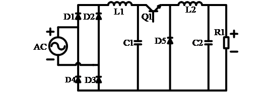
Figure 4. DBR with Buck and Input filter topology.
The Buck circuit is a step-down conversion circuit. Figure 4. DBR with Buck and Input filter topology consist of three parts: full-wave bridge rectifier circuit, input low-pass filter with buck circuit. The input low-pass filter circuit and buck circuit are described in detail in this article. The DBR circuit is covered in detail in the introduction of the Fundamental DBR with boost topology. The function of the input LC low-pass filter is to allow the DC component to pass through the full-wave rectifier and suppress the harmonic component so that it cannot pass through. According to the simulation results, the output voltage waveform after the LC low-pass filter is the DC component after rectification plus micro ripple. At this time, most of the interference has been filtered out and the DC frequency of the input buck circuit is higher.
As can be seen in Figure 4. DBR with Buck with Input filter topology, buck circuit consists of a triode, a diode, an inductor, and a capacitor, which are externally connected to the EV battery load. When the triode Q1 is switched on, the diode D5 is cut off, and the current flows through the inductor. The inductor current increases at a certain rate and stores a certain amount of energy. At the same time, the input current charges the EV battery and the capacitor C2. When the EV battery terminal voltage reaches the preset voltage, the triode Q1 is turned off, and there is no current input. When Q1 is switched on, the inductor accumulates a certain amount of energy and has the characteristic of holding, and then the inductor discharges the load to the EV battery. As time goes by, the stored power in the inductor gradually decreases. When the voltage of the EV battery terminal is lower than the preset voltage, the triode Q1 turns on and supplies power to the EV battery. When the voltage through the inductor and load is higher than the preset voltage, Q1 has turned off again and repeated constantly. Therefore, the output voltage fluctuates around the preset voltage value, but the fluctuation is small and the reciprocating frequency is fast, which can be ignored. In addition, it should be noted that the inductor voltage cannot immediately reach the preset voltage of the EV battery at the moment when Q1 is turned off. The working characteristic of the capacitor is that when its voltage is higher than the external voltage, the capacitor will discharge. But when the external voltage is higher than the capacitor voltage, the capacitor is charged. Therefore, when Q1 is turned off, the voltage at both ends of the capacitor is higher than the external voltage, and the capacitor is discharged. The capacitor charges the EV battery in a very short period of time. The depressurization process is complete.
As mentioned at the beginning of this section, the buck circuit is a step-down circuit that requires the input voltage to be higher than the preset output voltage. Therefore, when the preset voltage is higher than the input voltage, the buck circuit is no longer applicable. It can only be used for step-down, less general use, and the input current is intermittent, output ripple. Like a boost circuit, it has the advantages of high efficiency and small size. At the same time, a buck circuit has the advantage of continuous output current.
2.3. DBR with single-switch buck-boost topology
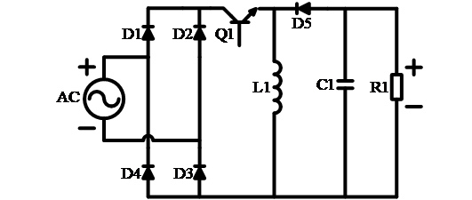
Figure 5. DBR with single-phase buck-boost topology.
Buck-boost converters may also be called up-and-down converters. The circuit is shown in Figure 5. DBR with Single-phase Buck-Boost topology is composed of a DBR circuit and a buck-boost circuit, which is the most simplified buck-boost circuit. It can be seen as the circuit after the buck circuit and boost circuit are connected in series and combined with the triode. The working principle of the Buck-boost circuit is that when the triode Q1 is switched on, the AC output voltage of the power supply is rectified and then the DC voltage is used to charge the inductor. In the charging process, the inductor voltage continuously increases and accumulates energy. At this time, the polarity of the inductor is positive up and negative down. Due to the presence of diode D5, the power supply cannot supply power to the capacitor C1 and EV battery load. when Q1 is switched on, the voltage at both ends of C1 is higher than the external voltage, so C1 charges the loaded EV battery. When Q1 is disconnected and the supply voltage cannot pass through, the capacitor and EV battery load are charged by the accumulated energy before the inductor. It should be noted that, due to the existence of the diode, the inductor current cannot flow out from the upper end, but only from the lower end, so the polarity of the inductor is negative up and positive down, so the polarity of the output voltage is opposite to the polarity of the input voltage. When Q1 has switched on again, the power supply voltage charges the inductor, and the EV battery load terminal is powered by C1. This process is repeated to supply power to the EV battery load.
Notably, in what way does buck-boost achieve this boost? At this time, it depends on the duty ratio of the PWM wave that controls the conduction or cutoff of the triode. If the duty ratio is greater than 1/2, the circuit is in a state of boost voltage; On the contrary, the circuit is in a step-down state. The buck-boost circuit has the advantages of low internal consumption, low-temperature drift, wide operating temperature range, stable output voltage and wide input voltage range. The most important point is that it can both boost and reduce voltage. The buck-boost circuit also has the disadvantage of large output ripple, so it is often used with the filter in practical applications to reduce the ripple.
2.4. DBR with cascaded buck-boost topology
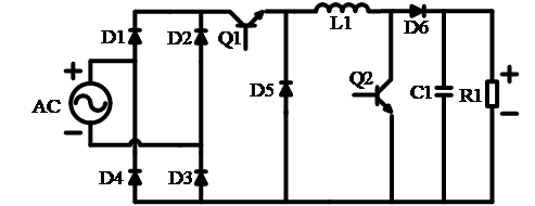
Figure 6. DBR with cascaded buck-boost topology.
Similarly, Figure 6. DBR with Cascaded Buck-Boost topology also shows the reader a buck-boost voltage lifting circuit, slightly different from the circuit shown in Figure 5. DBR with Single-phase Buck-Boost topology. As shown in Figure 6. Cascaded Buck-Boost topology, this paper first analyzes the first case. When Q1 is in an on-off state and Q2 is also in an on-off state, Q1 and Q2 are regarded as a wire. Then Q2 short-circuits D6, C1 and R1, and the current flows through Q1, L1 and Q2 in turn and returns to the negative terminal of the power supply. L1 builds up energy. When Q2 is in the off state, Q2 can be regarded as open, and the power supply and inductor are simultaneously charged to the capacitor C1, EV battery load. At this point, the boot process is complete, so the circuit is the boost circuit.
In the second case, when Q2 is off for a long period of time, Q2 is regarded as open. When Q1 is in the on-off state, the power supply current flows through the inductor L1 to charge the capacitor C1 and EV battery. L1 accumulates energy continuously as the current flows through L1. When Q1 is turned off, the current of the power supply cannot flow at this time. Due to the retention of inductance, the inductance is charged to the load end of capacitor C1 and EV battery. At this point, the step-down process is complete, so the circuit is buck step-down circuit.
Due to the presence of the buck circuit and boost circuit in the circuit, its disadvantage lies in the use of many components, and the turn-on and turn-off operations of triode Q1 and Q2 are complex and not concise enough. Its advantages are similar to those of the circuit shown in Figure 5. DBR with Single-phase Buck-Boost topology, which will not be discussed here.
2.5. DBR with SEPIC topology
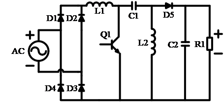
Figure 7. DBR with SEPIC topology.
The SEPIC circuit is one kind of chopper circuit, which will be analyzed in detail in this paper. First of all, when the triode Q1 is in the on-state, there are two loops in the circuit. the first loop is the power supply through the rectifier after flowing through the inductor L1, Q1 back to the negative terminal of the power supply, and the current flows through L1 for energy storage. The second loop is because when Q1 is off, the power supply has charged C1 voltage to equal the power supply voltage, and since Q1 is on at this time, the capacitor C1 discharges the energy storage inductor L2, which stores energy. At this point diode D5 is cut off, so only capacitor C2 can charge the EV battery load.
SEPIC chopper circuit has obvious advantages and disadvantages. It has the advantages of adjustable voltage, same polarity output, small input current pulsation, and easy expansion of output. Therefore, the SEPIC chopper circuit is widely used in elevating voltage converter circuits and PFC circuits. By observing the SEPIC circuit diagram, we can see that there are many circuit components, which are not easy to use, and the price is relatively high. Although the efficiency is high, it is still lower than the step-down converter. The SEPIC circuit also has high EMI and output ripple, so more attention should be paid to the layout of the circuit board.
2.6. DBR with cuk topology
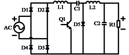
Figure 8. DBR with cuk topology.
The cuk circuit is also one of the basic chopper circuits, which can also be regarded as the series formation of time boost and buck circuit combined with audion, as shown in Figure 8. DBR with Cuk topology. Its working principle is as follows: when the triode Q1 is switched on, Q1 can be regarded as a wire. At this time there are two loops in the circuit. In the first loop, the current starts from the positive terminal of the power supply and flows through L1, which continuously stores energy along with the current flow. As Q1 is switched on, the current flows back to the negative terminal of the power supply from Q1. Since the current flows directly to capacitor C1 after passing L1 at the cutoff of Q1, C1 has been charged, and the polarity of the capacitor at this time is positive left and negative right. So the second loop is where the current is supplied by the capacitor C1, flows out of the positive side of the capacitor, flows through C2, returns to the negative side of C1, flows through C2 and L2, C2 is charged, and L2 is stored.
In the second case, when the triode Q1 is turned off, Q1 can be regarded as an open circuit. At this time, the first loop is the power supply current flowing through the inductor L1 and then to the capacitor c1. After charging C1 by the power supply, L1 returns to the negative terminal of the power supply through D5. Since the current flowing from C1 has already flowed through L2 when Q1 is switched on, L2 has stored energy. Therefore, due to the reverse cutoff property of the diode in the second loop, the current can only flow out from the left end of L2 and return to the right end of the inductor after flowing through C2, forming the second loop.
The advantage of the Cuk circuit is that the input and output terminals have inductance, can significantly reduce the input and output current pulsation, and output voltage can be lower than or higher than the input voltage. But the output polarity of the Cuk circuit is opposite to the input polarity, and the working principle and operation are more complicated.
2.7. DBR with zeta topology
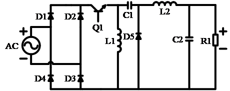
Figure 9. DBR with zeta topology.
A Zeta circuit can also be called a Zeta converter, which can be considered as a buck-boost circuit cascaded buck circuit, as shown in Figure 9. DBR with Zeta topology. Analysis of the working principle of the Zeta circuit can be divided into two cases: respectively triode Q1 on and off respectively. Firstly, the first case is analyzed: when the triode Q1 is switched on, the power supply current flows through the inductor L1 and returns to the negative terminal of the power supply, the power supply charges L1 at this time. At the same time, capacitor C1 needs to release the electric energy charged during the cutoff of the previous cycle Q1 to charge the inductor L2 and then flow to the load. In this case, there are two parallel loops in the circuit, the first loop is that the current from the power supply goes through the triode Q1, inductor L1 and then flows back to the negative terminal of the power supply. The second loop is the power supply through the triode Q1, C1, L2, and EV battery load back to the negative terminal of the power supply. The second case is that when the triode Q1 is off, the power supply cannot supply to the branch after Q1. At this time, the inductor L generates a positive down and negative up induced electromotive force and charges C1 through diode D5. Since the inductor L2 has been charged in the previous cycle, L2 charges the C2 and EV battery loads at this time. At this stage, there are also two loops in the circuit. In the first loop, the current flows out of the L1 positive terminal and returns to the L1 negative terminal after being charged by D5 and C1. The second loop is the current from the right end of L2, powering the EV battery load and returning to the left end of the inductor L2.
Zeta topology has the ability to raise and lower voltages. The capacitors and inductors at the output end of the circuit can also be regarded as LC low-pass filters, so the output ripples are small and the input and output voltages are of the same polarity. Zeta topology also has disadvantages. According to [4-5], the frequency characteristics of traditional Zeta converters are complex, which makes the design of closed-loop controllers difficult and unstable.
3. Modified topologies
3.1. Bridgeless boost-derived topology
As can be seen from the above, the traditional bridged boost topology has the disadvantages of high on-off loss and low efficiency, so the bridged boost topology mentioned in [6] can optimize these problems. According to the comparison with the fundamental full-wave bridge boost in [6], the fundamental full-wave bridge boost has more semiconductor devices working when the switch tube is on or off. When the current is large, the on-off loss of the semiconductor device increases correspondingly, resulting in lower efficiency. However, the number of semiconductor devices used by the half-bridge boost is smaller than that used by the traditional band-bridge boost when the switch tube is off or on, which can reduce the on-off loss of semiconductor devices and improve efficiency. The operating mode analysis section in [6] explains in detail the operation of the circuit in the on-off or off-off state of the switch tube within one cycle. It can be known that there are two loops in the circuit of the bridgeless boost topology in the on-off and off-off state of the switch tube, respectively powered by energy storage components or power sources for the load. From the perspective of circuit structure, the bridged boost introduced in [6] has the advantages of fewer components, a simple circuit structure, and higher efficiency than the traditional boost with Bridges. However, the output ripple is larger, resulting in greater interference of harmonic components.
3.2. Interleaved boost-derived topology
The reader is shown in [7] a staggered parallel booster topology, which can effectively solve the problems of high ripple currents and harmonic pollution in the traditional booster topology. The circuit structure shows that the modified boost topology retains the full-wave bridge and the rear circuit section can be seen as two switches controlling two separate boost circuits. By interpreting its operation, the reader can understand that the two switches S1, and S2 in this topology operate independently and that the circuit is a conventional boost circuit when each switch operates independently. One of the factors influencing its topological operating process is the duty cycle. [7] shows that the current characteristics of the circuit differ when the duty cycle is greater or less than 0.5, but that the superposition of the currents of the two states is able to reduce the input current ripple, at which point it can be deduced that the DC component of the waveform is proportionally higher and the harmonic component is lower, thus improving the power factor. Therefore, the topology introduced in [7] has the advantages of small current ripple, high power utilization, and low harmonic pollution, but the topology has multiple operating states with different duty cycles and a complex operating principle that is difficult to analyze.
3.3. Bridgeless buck-boost derived topology
In [8] the reader is shown one of a bridgeless buck-boost topology. From its operating principle, it is possible to operate the circuit in two different boost circuits and two different buck circuits, depending on the coordination of the conduction or switching off of different switching tubes. A comparison of the tables in [8] shows that a conventional buck-boost circuit with a full bridge uses more semiconductor devices than a bridgeless buck-boost circuit in either mode of operation, so a bridgeless buck-boost circuit is more efficient and uses fewer semiconductor devices, which results in relatively small conduction losses. However, just looking at the circuit, there are more components used in the circuit, and the design of the circuit board connection is more complex. Besides, its principle and operation are somewhat more complicated, and the purchase of components can be more expensive.
3.4. Bridgeless SEPIC-derived topology
Based on the traditional SEPIC circuit, the circuit structure has been continuously improved in order to improve its operating efficiency, so that the performance of the new circuit structure can meet or exceed the performance of the original traditional circuit. In [9], the reader is presented with a single switch-tube bridgeless SEPIC topology. According to the operating principle section in [9] this bridgeless SEPIC with a single-switch tube topology has two operating modes in one switching cycle, both of which are in the positive half-cycle of the AC input voltage. Due to the symmetry of the circuit, the operating principle when the supply voltage input is in the negative half-cycle is the same as when it is in the positive half-cycle. Similar to [8], the circuit shown in [9] is made to operate differently to improve its efficiency by switching on or off a switching tube, a slow recovery diode, and a fast recovery diode. Also, a comparison of the components used in this single-switch-tube bridgeless SEPIC topology with those used in conventional SEPIC circuits is shown to the reader in the form of a table in [9]. As can be seen from the icons, although the total number of components used in the single-switch-tube bridgeless SEPIC topology is higher and the number of diodes used is not very different from that of conventional SEPIC circuits, it is worth noting that fast recovery diodes are in the majority and slow recovery diodes are in the minority. In contrast, the traditional SEPIC circuit has a majority of slow recovery diodes. This comparison shows that the single-switch tube bridgeless SEPIC topology increases the efficiency of the circuit in terms of the type of components used. However, it also has the disadvantage of using a larger number of components and a more complex circuit structure and principle.
3.5. Bridgeless cuk topology
The conventional Cuk circuit structure and the operating principle have been shown to the reader in this paper, but there are many improved topologies derived from the Cuk circuit. The circuit diagram in [10] shows the reader a bridgeless Cuk topology, which consists of a combination of two parallel Cuk circuits with an overall top-down structure. According to the operating principle section of the bridgeless Cuk PFC converter in [10], the reader can understand that this bridgeless Cuk topology has three operating states, CCM, CRM, and DCM, respectively. Similar to [9], only when the supply voltage is at a positive half-cycle is analyzed in [10] due to the symmetry of the circuit. This circuit has three modes of operation when it is in the positive half-cycle, as can be seen from [10], where the circuit is in different states of operation depending on the on and off states of the switching tubes. The topology is capable of both boost and buck, but whether it is boost or buck depends on one important factor - the duty cycle. In [10], if the duty cycle is greater than 2/3, then the circuit is in boost mode; if the duty cycle is less than 2/3, then the circuit is in buck mode. Also, as stated in [9], this topology also has the advantage of being able to control the output ripple of the output voltage by selecting the appropriate switching frequency and output capacitor size. It also improves efficiency and power factor.
4. Comparison
Table 1. The comparison of PFC with DBR topologies.
Types | Number of semiconductor device | Advantages | Disadvantages | Form |
DBR with Boost | 6 (5 diodes with 1 switching tube) | Continuous input current, high efficiency, small size | Intermittent output current, large ripple, output noise, boost only | Step-up |
DBR with Buck and Input filter | 6 (5 diodes with 1 switching tube) | Continuous output current, high efficiency, small size | Intermittent input current, high output ripple, buck only | Step-down |
Table 1. (continued). | ||||
Types | Number of semiconductor device | Advantages | Disadvantages | Form |
DBR with Single-switch buck-boost | 6 (5 diodes with 1 switching tube) | Small internal consumption, small temperature drift, large operating temperature range, stable output voltage, wide input voltage range, ramp-up/down | Large output ripple, input and output current pulsation, causing electromagnetic interference | Adjustable voltage |
DBR with Cascaded buck-boost | 8 (6 diodes with 2 switching tubes) | Small internal consumption, small temperature drift, large operating temperature range, stable output voltage, wide input voltage range, ramp-up/down | Excessive components, the triode operation is complicated, not simple enough, the semiconductor device conduction loss is higher | Adjustable voltage |
DBR with SEPIC | 6 (5 diodes with 1 switching tube) | Ramp-up/down, co-polar output, low input current pulsation, easily scalable output | More circuit components, less easy to use and relatively expensive, lower efficiency, high EMI, large output ripple | Adjustable voltage |
DBR with Zeta | 6 (5 diodes with 1 switching tube) | Smaller output ripple, same polarity of input and output voltages, adjustable voltage | Complex frequency characteristics, difficulty to design closed-loop controllers | Adjustable voltage |
DBR with Cuk | 6 (5 diodes with 1 switching tube) | Significantly reduce the pulsation of the input and output currents, adjustable voltage | Opposite input and output polarity, provides less current | Adjustable voltage |
Table 2. The comparison of bridgeless PFC topologies.
Types | Number of semiconductor device | Advantages | Disadvantages | Form |
Bridgeless boost derived | 4 (2 diodes with 2 switching tubes) | Reduces on-state losses in semiconductor devices and increases efficiency | High interference, high EMI, and current sampling polarity may be inconsistent | Step-up |
Interleaved boost derived | 6 (6 diodes) | Small current ripple, high power utilization, low harmonic pollution | The duty cycle varies and there are multiple operating states, the operating principle is complex and difficult to analyze | Step-up |
Table 2. (continued). | ||||
Types | Number of semiconductor device | Advantages | Disadvantages | Form |
Bridgeless buck-boost derived | 7 (4 diodes with 3 switching tubes) | Relatively low conduction losses due to the use of fewer semiconductor devices | More components, more complex circuit board connections, more complicated principles and operation, high price | Adjustable voltage |
Bridgeless SEPIC derived | 6 (5 diodes with 1 switching tube) | Improved efficiency and power factor | A high number of components used, complex circuit structure, and principle | Adjustable voltage |
Bridgeless Cuk derived | 10 (8 diodes with 2 switching tubes) | Voltage can be raised and lowered to improve efficiency and power factor, and the output ripple of the output voltage can be controlled by adjusting the component parameters | Complex circuit structure and principle, a large number of components, complex circuit board wiring | Adjustable voltage |
The number of semiconductor devices used in each of the PFC topologies described above and their advantages and disadvantages are shown in Table 1 and Table 2.
As can be seen from Table 1. The comparison of PFC topologies and Table 2. The comparison of bridgeless PFC topologies, with comparison and the circuit diagrams shown in this paper, the fundamental full-wave bridge PFC topology and the circuit working principle are both relatively simple. However, the common band-bridge boost circuit or band-bridge buck circuit has a single function and can only boost or buck, which is a low utilization rate of the equipment and far from satisfying people's daily needs. Although the improved PFC topology with a bridge can achieve the voltage rise and fall function, there are still problems that need to be solved in the fundamental PFC topology with bridges. The diodes used in the traditional PFC topology are mostly slow recovery diodes and less fast recovery diodes are used, which increases the conduction loss of the semiconductor devices and reduces the efficiency. In addition, the traditional band bridge PFC topology also suffers from a lack of high power factor and large output voltage ripple. Therefore improved PFC topologies such as bridgeless, staggered parallel and others have been introduced. According to available research, some of the improved PFC topologies are able to achieve power factors of 0.95 or more. This means that the active power share is 95%, a figure that also shows that the improved PFC topology has led to a more efficient device, with higher utilization and the vast majority of the current being used for the load, rather than being lost to the line or used for the conversion of alternating magnetic fields on the line. And in the improved PFC topology, the number of semiconductor devices used in the improved PFC topology is comparable to the number of semiconductor devices used in the traditional PFC with bridge, but most of the diodes used in the improved PFC topology are fast recovery diodes and a smaller number of slow recovery diodes are used, so many of the improved PFC topologies improve the circuit structure while reducing the semiconductor devices at this point in the use of components. The on-state losses of the semiconductor devices are reduced at this point of use, further improving efficiency and power factor. Although the efficiency of the improved PFC topology is improved, if one looks only at the circuit diagram, one finds that the circuit structure of the improved topology is most complex. The alternating operation of the power supply and different energy storage elements during operation and the existence of different loops in the circuit one state are the two factors that make the circuit more complex to work with. The complex wiring adds difficulty to the design of the circuit board.
5. Conclusion
This paper gives an overview of the structure and operation of the EV battery charger and some circuit diagrams of the relevant topologies for power factor correction and their operating principles, advantages and disadvantages. It can be seen that the size of the power factor will directly determine the efficiency of the electrical equipment. If the power factor is high, the efficiency and utilization rate of the equipment is high; if the power factor is low, the efficiency and utilization rate of the equipment is low and the proportion of reactive power is relatively high, so you can also roughly tell from this value whether the electrical equipment is good or bad. In future research, it is suggested that research can be carried out in the direction of optimizing the circuit structure and appropriately selecting semiconductor devices with low on and off losses to further improve efficiency. At the same time, the variety and usefulness of PFC topologies can be further broadened so that they can be applied to more different scenarios and improve utilization.
References
[1]. Yao Xin. Research on power factor correction technology of electric vehicle on-board charger [D]. Nanjing Normal University,2017.
[2]. Yi Hanqing. Exploration of pure electric vehicle power battery and charging technology [J]. Special Purpose Vehicle, 2022, 12: 44-46.
[3]. Wang Yuanqing,Li Hongmei. PFC AC/DC converter design for electric vehicle on-board chargers [J]. Application of Electronic Technique, 2015, 41(2): 152-155, 159.
[4]. Wang Shudong,Xu Zigui,Gao Xiang,Ding Yanjun,Wang Huanyu. Stability study of voltage feedback type Zeta chopper circuit [J]. Journal of Lanzhou University of Technology, 2018, 44(06): 92-95.
[5]. Xu Bangxian,Liu Xiaobo,Han Xiangmin et al. Parameter optimization method of coupled inductive Zeta converter [J]. Electronic Science and Technology, 2023, 36 (01) : 88-94.
[6]. Wang Danshu,Yi Jia'an,Dong Zhen et al. Single-cycle control of a bridgeless Boost PFC converter with ripple suppression unit [J]. Journal of Guangxi Normal University (Natural Science Edition), 2022, 40 (04) : 47-57.
[7]. Zhou Jiawei,Chen Zhuanhong,Lei Zhiheng. Technical study of interleaved parallel Boost PFC circuits [J]. Ship Power Technology, 2020, 40 (03) : 48-51.
[8]. Liu H-P, Wang W, Liu Y-G. Research on a new bridgeless Buck-Boost PFC converter [C]. Proceedings of the 3rd Academic Forum on Frontier Issues in Electrical Technology. 2007:32-37.
[9]. Ma Hongbo, Zheng Cong, Yu Wensong, et al. Single-switch tube bridgeless SEPIC PFC converter [J]. Power Automation Equipment, 2014, 34(4):72-77.
[10]. Shen Yanxia,Cai Chengchao,Li Jiacheng. A high power factor bridgeless Cuk PFC converter [J]. Journal of Electrical Machines and Control, 2018, 22 (12) : 93-98.
Cite this article
Zhong,Y. (2023). State-of-the-art power factor correction in EV charger. Applied and Computational Engineering,10,221-232.
Data availability
The datasets used and/or analyzed during the current study will be available from the authors upon reasonable request.
Disclaimer/Publisher's Note
The statements, opinions and data contained in all publications are solely those of the individual author(s) and contributor(s) and not of EWA Publishing and/or the editor(s). EWA Publishing and/or the editor(s) disclaim responsibility for any injury to people or property resulting from any ideas, methods, instructions or products referred to in the content.
About volume
Volume title: Proceedings of the 2023 International Conference on Mechatronics and Smart Systems
© 2024 by the author(s). Licensee EWA Publishing, Oxford, UK. This article is an open access article distributed under the terms and
conditions of the Creative Commons Attribution (CC BY) license. Authors who
publish this series agree to the following terms:
1. Authors retain copyright and grant the series right of first publication with the work simultaneously licensed under a Creative Commons
Attribution License that allows others to share the work with an acknowledgment of the work's authorship and initial publication in this
series.
2. Authors are able to enter into separate, additional contractual arrangements for the non-exclusive distribution of the series's published
version of the work (e.g., post it to an institutional repository or publish it in a book), with an acknowledgment of its initial
publication in this series.
3. Authors are permitted and encouraged to post their work online (e.g., in institutional repositories or on their website) prior to and
during the submission process, as it can lead to productive exchanges, as well as earlier and greater citation of published work (See
Open access policy for details).
References
[1]. Yao Xin. Research on power factor correction technology of electric vehicle on-board charger [D]. Nanjing Normal University,2017.
[2]. Yi Hanqing. Exploration of pure electric vehicle power battery and charging technology [J]. Special Purpose Vehicle, 2022, 12: 44-46.
[3]. Wang Yuanqing,Li Hongmei. PFC AC/DC converter design for electric vehicle on-board chargers [J]. Application of Electronic Technique, 2015, 41(2): 152-155, 159.
[4]. Wang Shudong,Xu Zigui,Gao Xiang,Ding Yanjun,Wang Huanyu. Stability study of voltage feedback type Zeta chopper circuit [J]. Journal of Lanzhou University of Technology, 2018, 44(06): 92-95.
[5]. Xu Bangxian,Liu Xiaobo,Han Xiangmin et al. Parameter optimization method of coupled inductive Zeta converter [J]. Electronic Science and Technology, 2023, 36 (01) : 88-94.
[6]. Wang Danshu,Yi Jia'an,Dong Zhen et al. Single-cycle control of a bridgeless Boost PFC converter with ripple suppression unit [J]. Journal of Guangxi Normal University (Natural Science Edition), 2022, 40 (04) : 47-57.
[7]. Zhou Jiawei,Chen Zhuanhong,Lei Zhiheng. Technical study of interleaved parallel Boost PFC circuits [J]. Ship Power Technology, 2020, 40 (03) : 48-51.
[8]. Liu H-P, Wang W, Liu Y-G. Research on a new bridgeless Buck-Boost PFC converter [C]. Proceedings of the 3rd Academic Forum on Frontier Issues in Electrical Technology. 2007:32-37.
[9]. Ma Hongbo, Zheng Cong, Yu Wensong, et al. Single-switch tube bridgeless SEPIC PFC converter [J]. Power Automation Equipment, 2014, 34(4):72-77.
[10]. Shen Yanxia,Cai Chengchao,Li Jiacheng. A high power factor bridgeless Cuk PFC converter [J]. Journal of Electrical Machines and Control, 2018, 22 (12) : 93-98.