


1. Introduction
All discrete components made of semiconductor materials are referred to as transistors. Transistors are useful for a wide range of analog and digital applications scenarios. As one of the most critical components of modern electrical appliances, transistors are used on a large scale because they can be mass-produced at very low cost per unit. Complementary metal oxide semiconductor(CMOS) has the basic unit circuit inverter consists of N-channel and P-channel MOS transistors. These two kinds of transistors are complementary in physical characteristics and can Implement specific logic functions of integrated circuits(IC) [1].
In recent years, CMOS technology is widely used in electronics fields. It is common to integrate substantial number of CMOS devices in an Integrated Circuit [2]. There is a principle proposed by Gordon Moore for CMOS technology development, it is“Moore’s Law”. The principle indicates that the number of components in an IC will be doubled every 18 months for at least a decade [3]. The number of transistors in ICs is increasing due to the improvement of chip manufacturing and the demand for functional diversity of chips [2]. However, many transistors inevitably bring power consumption and latency problems [1]. Therefore, designers are expected to complete better circuit designs to make the chip in carrying more and more transistors, but also have good performance [4-6]. For this reason, there are many researchers trying to find solutions for lower energy consumption and higher speed [5,7].
Some proven methods have also been proposed and published, providing IC designers with great ideas to optimize their circuit designs and broaden their thinking about circuit optimization. These methods have also had a significant impact on the growth of the IC field. There are some examples. Hybrid magnetic tunnel junction (MTJ)/CMOS circuits based on logic memory (LIM) structures are efficient way found and used for various logic gates to lower power loss by cutting down on the number of transistors [7]. The Sine-Cosine Algorithm (SCA) meta-heuristic search algorithm is an algorithm that converges these solutions to the best solution by creating some initial candidate solutions chosen at random and using a sine and cosine-based mathematical model. Using this algorithm for circuits of a CMOS differential amplifier and a CMOS operational amplifier with two stages are optimized in terms of transistor size to reduce the area occupied by transistors in the circuit. This algorithm is used to optimize the transistor size of the CMOS differential amplifier circuit and two-stage CMOS operational amplifier circuit to reduce the area occupied by transistors in the circuit and to improve the design specifications [8]. A multi-objective optimization algorithm is called Non-Dominated Sorting Genetic Algorithm (NSGA-II) for optimizing CMOS voltage reference circuit parameters. This proposed initial population generation scheme with artificial optimal solutions and special adaptation functions based on the characteristics of CMOS voltage reference circuits to increasing the rate of convergence and effectiveness of the optimization [9].
This paper summarizes several methods circuit structures to optimize the transistor size, namely Manchester Carry Chain [10], Variable-stage effort Tapered Buffers (VTB) [11], Hybrid Flower Pollination Algorithm(HFPA) [12]. Based on the application objects and scenarios of these methods, according to first introducing the core unit, model or algorithm of each method, then analyzing the direction and strategy of circuit optimization by methods such as circuit analysis, and finally obtaining the optimal size of transistors in different cases by specific parameters such as logic effort, and finally simulating and emulating by means of simulation software, etc. The indexes of component parameters, circuit power consumption and speed of the optimized circuit are obtained and compared with the data before optimization. After optimization, the overall performance of the circuit is significantly improved, which also shows that transistor size optimization has great value and significance for IC circuit design.
2. Principle analysis of sizing technology
The size of the transistor can be used to optimize the speed of the circuit. The criteria for pure delay optimization are not the same as those for power-delay product (PDP) optimization. Delay decreases monotonically as the size of the transistors or gates increases, but this is not the case with PDPs. And since power issues in today's IC designs are becoming increasingly important, it is crucial to establish the appropriate transistor size for achieving the demands for speed and power savings [13].
For Manchester carry chain, all domino stage output nodes are precharged to Vdd during the precharge phase (Φ=0). The same node will receive the incoming value from the preceding stage if the propagation signal Pk of the kth stage is strong during the evaluation phase as opposed to being forced to logic 0 by the generating signal (Gk) of the kth stage. The MCC outputs are equal to the number of adder levels, one for each level, and each level's inputs are the propagation and generation signals. While MCC requires a redundant stage to obtain the input feed of the first stage and as a clock signal, MCC estimates the carry for all stages based on the propagation and generation signals determined in advance. From the first step to the last stage, the ripple carry structure's critical path is transmitted in order to determine the final result, which is then combined with the sum bit. The ripple carry adder's critical path is calculated as:
\( {t_{adder}}=(N-1){t_{carry}}+{t_{sum}} \) (1)
\( {t_{carry}} \) and \( {t_{sum}} \) are related to the transmission delay of a stage, and The number of phases is N [10].
For Variable-stage effort Tapered Buffers (VTB), it has a very significant advantage over the conventional Tapered Buffer (FTB) that uses Fixed-stage effort. the stage effort hi of the ith inverter gate in the FTB is defined as the ratio between its load and its input capacitance. With optimal performance phase effort, the FTB will achieve minimum delay at the cost of large energy. A fixed phase effort leads to a linear increase in delay and a nonlinear decrease in energy, which reduces the efficiency of the energy-delay tradeoff. In contrast, in VTB, different inverters are allowed to have different stage efforts hi, so hi is not fixed and the designer can optimize for a given energy-delay target during the circuit design process. In contrast, VTB is more design area-efficient and also achieves smaller delay. With the same delay as FTB, VTB consumes less power [11,14].
Hybrid Flower Pollination Algorithm is a hybrid FPA algorithm generated by combining two meta-heuristics, Particle Swarm Optimization(PSO) and FPA, which provides a better solution for device sizing [12]. PSO is an optimization algorithm that social organizations or animal groups inspire. The social group is named a swarm and each individual in the swarm is called a particle. In the initial state, the particles are randomly scattered in the space and the feasible solution to the optimization problem is represented by the position of the particles in the optimization space. Each particle can search for the best particle at that time and then dynamically change the location as well as the rate of motion of the particle according to the known individual optimum and the global optimum [12,13,14].
3. Discussion of sizing methods
3.1. Manchester carry chain
The Manchester Carry Chain is a circuit structure commonly used in adder design. The next section describes the circuit optimization techniques for this structure as well as the specific calculation of circuit parameters and circuit simulation. Each stage of the Manchester Carry Chain can be thought of as a cascade of three components: pass transistors, CMOS dynamic logic, and an inverter. The following is a technical analysis of the size of each module:
For Inverter: For MCC, the rising edge of the output signal is preferred over the falling edge. Therefore, the size of the non-critical NMOS can be reduced in order to reduce the logical effort of the capacitance of the Inverter's input in its entirety. By comparing the logic effort of Unskewed inverter and Hi-Skewed inverter, it is found that the input capacitance and delay of Hi-Skewed inverter is smaller. So Hi-Skewed inverter sizing technology is chosen.
For CMOS Dynamic Logic: The pre-charge and assessment phases form the foundation for how the dynamic circuit functions. The clock-controlled pMOS is turned on during the precharge phase when the clock signal is low and the output node voltage is brought up to Vdd. The clock is set to high during the assessment phase, and the pMOS is turned off. At this point, the output is dependent on the signal's production or propagation. The precharge transistor's width should be kept to a minimum to minimize the capacitive load and parasitic effects on the input, while the nMOS's size can be increased to enable quicker evaluation.
For Pass Transistor: The El-more delay model states that the transistor nearest to the input is the widest and that the pass transistor can be thought of as a resistor. Four route transistors make up the critical path, which moves the Carry signal forward. Based on the idea of progressive size, the critical path's size is established. The size of the pass transistor is therefore smallest in the final carry stage, greatest in the transistor farthest from the output, and the width of the path transistor is cut in half for each passing stage. The time constant and resulting delay are decreased when the transistor width is increased. Figure 1 shows the sizing techniques for each block.
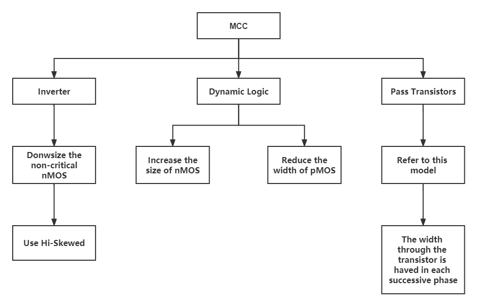
Figure 1. Methods for sizing each MCC block.
Each transistor has a fixed length of 180 nm (gpdk180). when the pMOS to nMOS width proportion is 4:1, a symmetric inverter characteristic can be found by analyzing the inverter parameters in Cadence Virtuoso. It can be assumed that a 250 nm wide transistor has a capacitance of 2 fF and the stage's related output capacitance is 100 fF as the smallest permissible transistor width in 180 nm technology is 400 nm. Figure 2 shows the flow of sizing calculation for one stage.
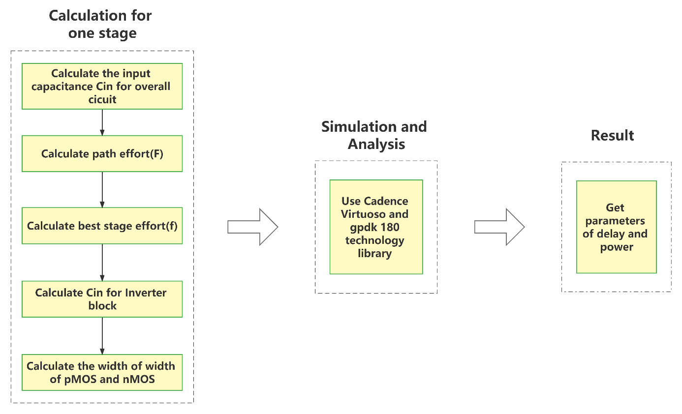
Figure 2. Flowchart for sizing calculation for one stage.
As demonstrated in Tables 1 and 2, the conclusions can be drawn by summarizing and analyzing the circuit parameters collected from the simulation.
Table 1. Optimization results. |
Parameter | Without optimization | With optimization | Conclusion |
Power | 15.52uW | 17.18uW | 9.6% Increase |
Delay | 0.803ns | 0.493ns | 18.8% Decrease |
Table 2. Layout results. |
Parameter | Pre Layout | Post Layout | Conclusion |
Power | 17.18uW | 20.2uW | 15% Increase |
Delay | 0.493ns | 0.688ns | 31.2% Increase |
The data in Table 1 and Table 2 are obtained from the Simulation and Analysis step in Figure 2. The simulation results visually illustrate the effect of optimization and rewiring on delay and power.
These findings show that optimizing the circuit using MCC and sizing techniques can indeed reduce delays and power very well. Still, special attention should be paid to the increase in delays and power caused by routing parasitics during wiring.
Adders play an essential and key role in many algorithms of computers and are very important and commonly used circuit structures. It is used not only in computers but also in processors for various operations. Adders are used in circuits to reduce the number of transistors [15]. MCC is an excellent circuit logic and sizing technology that can be used for adders to reduce delay and power effectively. Therefore, this research can be considered valuable and useful for circuit designers.
3.2. Optimized VTBs
This system transistor sizing approach that optimizes the stage effort and number of stages of the VTB to meet a specific energy-delay trade-off. This approach is technology independent and applicable to a wide range of voltages.
The energy-delay sensitivity function of the buffer is first obtained by generalizing the sign of the logical effort to the case of an arbitrary energy-delay tradeoff and VTB, which depends on the size wi of the ith inverter and the logical effort of the ith stage. It follows from this function that when hi is monotonically increasing, it is always possible to optimize the circuit to reduce energy consumption by optimizing the transistor size wi, but doing so results in higher delay. A fixed factor c is defined here which sets the rate of increase of electrical power for each buffer stage according to a pseudo-exponential trend. The buffer delay and energy depend on only three parameters: the constant c, the number of stages N, and the buffer fan-out \( {C_{L}}/{C_{in }} \) , hi, N, and c are interdependent for the optimization of hi, so for the analytical evaluation of hi, N and c are initially evaluated numerically in a technology-independent manner. This optimization was performed for a various fan-out volume interface specifications and energy-delay design objectives. Each energy-delay design objective is defined as the buffer size that minimizes the generalized energy-delay product \( {E^{a}}{D^{b}} \) metric, where a and b are integers greater than or equal to 1. A larger a(b) means that energy (delay) will have a higher priority than delay (energy) in the optimization process. minimization of the \( {E^{a}}{D^{b}} \) metric explicitly includes energy in the design process, allowing a reasonable balance between design points and performance. This will ensure that the given circuit design requirements are achieved while minimizing energy consumption.
In order to have a general framework for optimization in a technology and voltage-independent manner by minimizing each \( {E^{a}}{D^{b}} \) metric, a technology/voltage independent expression for energy and delay is used. The numerical optimization to evaluate N and c is based on the Newton-Raphson algorithm. Using this algorithm, fan-out \( {C_{L}}/{C_{in }} \) was generated from 50 to 1,000, and five design metrics \( {E^{a}}{D^{b}} \) (a, b = 1...3) for the VTB configuration. As the load increases, the optimal c decreases monotonically while the optimal N increases. c decreases proportionally to \( {C_{L}}/{C_{in }} \) -0.8 with a scaling constant that depends on the target \( {E^{a}}{D^{b}} \) metric. The flow of frame acquisition is showed in Figure 3.
The values of c and N and the optimal configuration of the FTB are shown in Table 3. The results in the table can be applied to any technology and above-threshold voltage. The optimum transistor size can also be calculated from the data in Table 3.
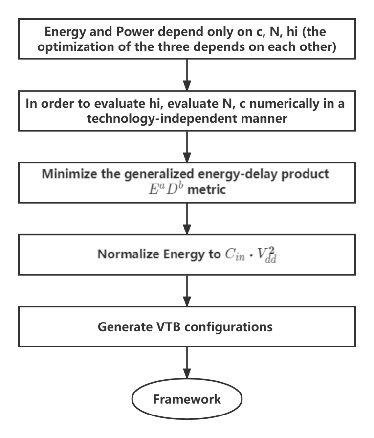
Figure 3. Flowchart for frame acquisition.
Table 3. Optimal c and N versus fanout and design target.
|
| FTB | ||||||||||
\( {C_{L}}/{C_{in }} \) |
|
|
|
|
|
|
|
|
|
|
|
|
50 | 1.255 | 0.795 | 0.291 | 0.134 | 0.087 | 2 | 2 | 3 | 3 | 3 | 3 | 3.68 |
100 | 0.696 | 0.419 | 0.187 | 0.088 | 0.049 | 3 | 3 | 3 | 3 | 4 | 4 | 3.16 |
200 | 0.423 | 0.26 | 0.104 | 0.047 | 0.03 | 3 | 3 | 4 | 4 | 4 | 5 | 2.89 |
300 | 0.317 | 0.177 | 0.077 | 0.035 | 0.023 | 3 | 4 | 4 | 4 | 4 | 5 | 3.13 |
400 | 0.259 | 0.141 | 0.062 | 0.029 | 0.017 | 3 | 4 | 4 | 4 | 5 | 5 | 3.31 |
500 | 0.196 | 0.118 | 0.053 | 0.022 | 0.014 | 4 | 4 | 4 | 5 | 5 | 5 | 3.47 |
600 | 0.169 | 0.103 | 0.046 | 0.019 | 0.012 | 4 | 4 | 4 | 5 | 5 | 6 | 2.90 |
700 | 0.15 | 0.091 | 0.038 | 0.017 | 0.011 | 4 | 4 | 5 | 5 | 5 | 6 | 2.98 |
800 | 0.134 | 0.082 | 0.034 | 0.015 | 0.01 | 4 | 4 | 5 | 5 | 5 | 6 | 3.05 |
900 | 0.122 | 0.075 | 0.031 | 0.014 | 0.009 | 4 | 4 | 5 | 5 | 5 | 6 | 3.11 |
1,000 | 0.113 | 0.069 | 0.029 | 0.013 | 0.008 | 4 | 4 | 5 | 5 | 5 | 6 | 3.16 |


The data in Table 3 are the VTB configurations obtained based on the Newton-Raphson algorithm after the Normalize Energy to \( {C_{in}}\cdot V_{DD }^{2} \) step in Figure 3.
Applying the above optimizations, the VTB can reduce energy by 30% in design goals where energy is as important as or more important than latency. In contrast, VTB can reduce energy by 10-20% in design goals with low latency. Therefore, it can be concluded that VTB allows significant energy reduction with a moderate delay penalty.
Buffers are widely used in CMOS circuits to give the circuit a stable output, better voltage transfer characteristics and a steeper output curve. However, because of their large size, they significantly impact the circuit’s overall energy consumption. They also have a large delay, thus significantly impacting the overall system performance. This optimization method can meet circuit design requirements while enabling significant reductions in energy consumption. The design strategy allows circuit designers to handle the energy-delay tradeoff of CMOS buffers in a straightforward and technology-independent manner, determining the optimal transistor size and effectively improving design efficiency. Therefore, it is a very practical transistor sizing optimization method that can be widely used in circuit design [11].
3.3. Hybrid flower pollination algorithm
Circuit optimization techniques can lead to better circuit performance for circuit design problems. FPA can fall into local rather than global optimality, so FPA is not the best method to apply to circuit optimization. Researchers have combined FPA and PSO algorithms, for sizing op amps. This hybrid FPA absorption combines the advantages of each of the two algorithms: the exploration capability of FPA and the exploitation capability of PSO in order to obtain a globally optimal solution. The first stage of this HFPA is PSO, using which the fitness value of each particle can be calculated and then updated for \( {p_{best}} \) and \( {g_{best }} \) , and the \( {g_{best }} \) obtained in this stage is in turn used as the initial best solution for the next stage of the FPA algorithm (B). In this stage, each particle is locally pollinated or globally pollinated. And the value of each particle's fitness is recalculated making use of the cost function. If this result is better than the previous one, the \( {p_{best}} \) and \( {g_{best }} \) are updated to obtain the final global optimal solution of HFPA.
Operational amplifier circuit construction with two stages is shown in the Figure 4.
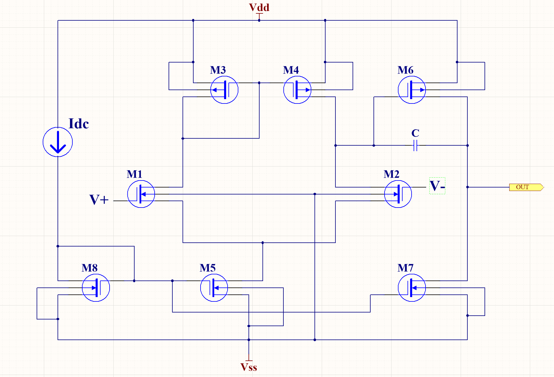
Figure 4. Operational amplifier circuit construction with two stages.
The flow of the specification of the circuit in Figure 4 is converted to the objective function and constraints as shown in Figure 5.
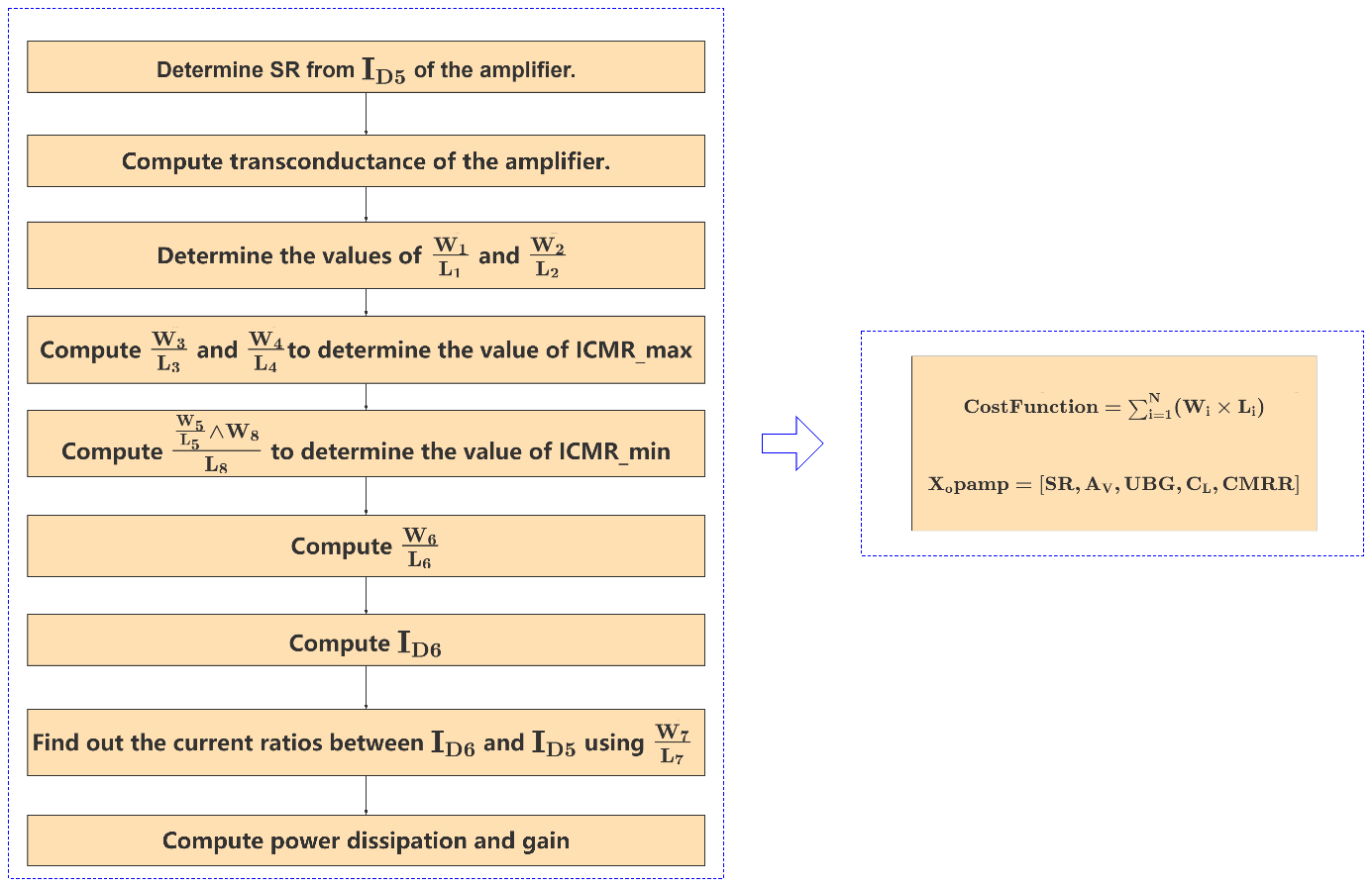
Figure 5. Flowchart for specification of op amp converted into the objective function and constraints.
With the flow in Figure 5, the cost function and constraint function of the amplifier circuit can be obtained, and then the HFPA algorithm can be used to obtain the optimal size of the transistor and operational amplifier design parameters, and this process is shown in Figure 6.
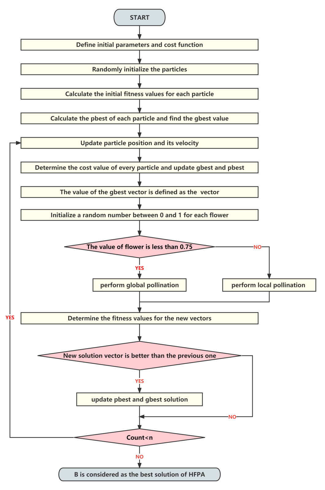
Figure 6. Flowchart for obtaining the optimal size of the transistor and operational amplifier design parameters with HFPA.
The HFPA-based operational amplifier circuit parameters can be obtained by the above method and simulation to meet the specifications and reduce the power consumption. Table 4 lists the ideal transistors, and Table 5 lists the requirements for creating CMOS operational amplifiers.
Table 4. Size considerations for transistors used in operational amplifiers. | ||||||||
Circuit parameters | Values | Units | ||||||
\( {W_{1}}/{L_{1}} \) | \( 12/2 \) | um | ||||||
\( {W_{2}}/{L_{2}} \) | \( 12/2 \) | um | ||||||
\( {W_{3}}/{L_{3}} \) | \( 2.8/0.18 \) | um | ||||||
\( {W_{4}}/{L_{4}} \) | \( 2.8/0.18 \) | um | ||||||
\( {W_{5}}/{L_{5}} \) | \( 3.8/0.18 \) | um | ||||||
\( {W_{6}}/{L_{6}} \) | \( 31/0.18 \) | um | ||||||
\( {W_{7}}/{L_{7}} \) | \( 37.5/0.50 \) | um | ||||||
\( {W_{8}}/{L_{8}} \) | \( 3.8/0.18 \) | um | ||||||
\( {C_{L}} \) | 800 | um | ||||||
\( {I_{bias }} \) | 20 | um | ||||||
Table 5. Achieved performance specifications for a CMOS operational amplifier design. | ||||||||
\( \begin{matrix} Design \\ specifications \\ \end{matrix} \) | Specifications | PSO | \( \begin{matrix} Convex \\ optimization \\ \end{matrix} \) | \( \begin{matrix} Proposed \\ method \\ \end{matrix} \) | ||||
UGB (MHz) | \( \gt 5 \) | 5.32 | 86 | 5.252 | ||||
\( \begin{matrix} Load capacitance \\ (pF) \\ \end{matrix} \) | \( ≥10 \) | 10 | 3 | 10 | ||||
Gain (dB) | \( \gt 65 \) | 63.8 | 89.2 | 69.80 | ||||
Slew rate \( (V/μs) \) | \( ≥10 \) | 11.13 | 88 | 10.38 | ||||
Phase margin (°) | \( \gt 60 \) | 66.55 | 60 | 66.45 | ||||
Area \( (μ{m^{2}}) \) | \( \lt 300 \) | 265 | 8200 | 252 | ||||
\( \begin{matrix} Power dissipation \\ (uW) \\ \end{matrix} \) | \( ≤3000 \) | 2370 | 5000 | 712.2 | ||||
CMRR (dB) | \( \gt 80 \) | 83.74 | 92.5 | 88 | ||||
The amplifier designed in this way can be well suited for IoT terminal devices. In addition, this circuit design method provides an algorithm that can calculate the optimal transistor size for a given amplifier specification, which can effectively reduce the power consumption and chip area of the amplifier circuit and effectively solve the problem of large-scale analog circuit design. Therefore, it has a broad application prospect and great research significance in the future research in the field of analog integrated circuits.
3.4. Comparison
Table 6 compares the above three methods.
MCC is a circuit structure for adders. Adder is an operation module that almost all processors need to have. Many designers are also happy to use MCC in the design of adder circuits because of its low power consumption. In order to make MCC faster, size optimization techniques are used for it. Its optimization method uses different optimization techniques for its different circuit parts. For Inverter, Hi-Skewed technique is used. For Dynamic logic, nMOS’s size is increased and pMOS’s width is reduced. For the Pass transistor, the EI-more delay model is used. Using these techniques, the delay is reduced by 19%.
Table 6. Comparison of the three methods. | |||
MCC | VTB | HFPA | |
Application object | Adders | CMOS Buffer | CMOS Operational Amplifiers |
Research Scene | CMOS Processor | CMOS Systems | IoT end-node devices |
Method characteristics | Use different sizing technology for different components | Develop the technology-independent Energy-Delay model | Mix the both PSO and FPA metaheuristics |
VTB is a common buffer with variable stage effort. The performance of the circuit as a whole is significantly influenced by the buffer's design. In order to find the optimal transistor size and other circuit parameters, an Energy-Delay framework model is constructed. This technology-independent model allows designers to quickly find the most appropriate circuit parameters and optimize transistor sizes. The application of this framework allows the circuit to reduce energy consumption better while meeting design goals.
HFPA is a hybrid algorithm for optimizing CMOS operational amplifiers, which can effectively solve the transistor size problem. HFPA is a hybrid of PSO algorithm followed by FPA algorithm, which finds the optimal solution of the objective function by multiple iterations. In the circuit design, it is to find the optimal circuit parameters. This algorithm can reduce the amplifier circuit power consumption, improve the circuit gain and reduce the chip area. Although this amplifier is mainly used in IoT terminal devices, the research of this algorithm is also useful for solving large-scale analog circuit design problems.
4. Conclusion
Transistors are the basic building blocks of ICs, and integrating a huge number of transistors on a single chip inevitably leads to problems of power consumption and delay problems. Researchers have been working to find more effective and applicable transistor sizing technology. The three approaches summarized in this paper can significantly improve circuit performance and reduce circuit specifications. Both optimized MCC and VTB-based Energy-Delay framework models can significantly reduce latency and power consumption. The HFPA algorithm for CMOS operational amplifiers can significantly reduce many circuit design parameters including CMRR, area, and power dissipation. More importantly, these three methods have strong general applicability and can be extended to various circuit optimization scenarios to achieve better circuit performance, and the chip products designed using this method are more competitive in the market. In the computer field, one of the most important factors in judging the performance of a computer is its CPU performance. And the development of microprocessors will drive the development of computers. Whenever a new microprocessor appears, it will lead to the corresponding development of other components of the computer system. Transistor sizing technology is crucial for enhancing the functionality of semiconductors and has great research value and application prospects. The breakthrough of this technology may bring great progress in human society's technology level.
References
[1]. Kumar P, Bhandari N S, Bhargav L, Rathi R and Yadav S C 2017 Design of low power and area efficient half adder using pass transistor and comparison of various performance parameters. 2017 International Conference on Computing, Communication and Automation (ICCCA).
[2]. Gupta P, Gourishetty S, Mandadapu H and Abbas Z 2019 PVT variations aware robust transistor sizing for power-delay optimal CMOS digital circuit design. 2019 IEEE International Symposium on Circuits and Systems (ISCAS).
[3]. Wong H 2021. On the CMOS device downsizing, more Moore, more than Moore, and more-than-moore for more Moore. 2021 IEEE 32nd International Conference on Microelectronics (MIEL).
[4]. Hasan M, Saha U K, Sorwar A, Dipto M A, Hossain M S and Zaman H U 2019 A novel hybrid full adder based on gate diffusion input technique, transmission gate and static CMOS logic. 2019 10th International Conference on Computing, Communication and Networking Technologies (ICCCNT).
[5]. Mistry T and Yadav S 2022 Analysis of leakage power reduction using lector and ONOFIC technique in clock gated flip-flop. 2022 2nd Asian Conference on Innovation in Technology (ASIANCON).
[6]. Iyengar S and Shrinivasan L 2018 Power, performance and area optimization of I/O Design. 2018 International Conference on Inventive Research in Computing Applications (ICIRCA).
[7]. Barla P, Shet D, Joshi V K and Bhat S 2020 Design and analysis of Lim hybrid MTJ/CMOS logic gates. 2020 5th International Conference on Devices, Circuits and Systems (ICDCS).
[8]. Majeed M M and Rao P S 2017 Optimization of CMOS analog circuits using sine cosine algorithm. 2017 8th International Conference on Computing, Communication and Networking Technologies (ICCCNT).
[9]. Huang H, Zeng Y, Liao J, Chen R and Tan H 2018 Performance optimization for the CMOS voltage reference circuit based on NSGA-II. 2018 IEEE Asia Pacific Conference on Circuits and Systems (APCCAS).
[10]. A H and Sethi S 2019 Sizing techniques for delay optimisation of 4-bit dynamic CMOS manchester carry chain. 2019 International Conference on Vision Towards Emerging Trends in Communication and Networking (ViTECoN).
[11]. Lin L, Quang K T and Alioto M 2017 Transistor sizing strategy for simultaneous energy-delay optimization in CMOS buffers. 2017 IEEE International Symposium on Circuits and Systems (ISCAS).
[12]. Sasikumar A, Subramaniyaswamy V, Jannali R, Srinivasa Rao V and Ravi L 2022 Design and area optimization of CMOS operational amplifier circuit using hybrid flower pollination algorithm for IOT end-node devices. Microprocessors and Microsystems, 93, 104610.
[13]. Duan M 2018 Short-time prediction of traffic flow based on PSO optimized SVM. 2018 International Conference on Intelligent Transportation, Big Data & Smart City (ICITBS).
[14]. SKefi S, Rokbani N, Kromer P and Alimi A M 2016 Ant supervised by PSO and 2-Opt algorithm, as-PSO-2OPT, applied to traveling salesman problem. 2016 IEEE International Conference on Systems, Man, and Cybernetics (SMC).
[15]. Koyada B, Meghana N, Jaleel M O and Jeripotula P R 2017 A comparative study on Adders. 2017 International Conference on Wireless Communications, Signal Processing and Networking (WiSPNET).
Cite this article
He,X. (2023). Design of CMOS circuits through transistor sizing techniques. Applied and Computational Engineering,12,1-12.
Data availability
The datasets used and/or analyzed during the current study will be available from the authors upon reasonable request.
Disclaimer/Publisher's Note
The statements, opinions and data contained in all publications are solely those of the individual author(s) and contributor(s) and not of EWA Publishing and/or the editor(s). EWA Publishing and/or the editor(s) disclaim responsibility for any injury to people or property resulting from any ideas, methods, instructions or products referred to in the content.
About volume
Volume title: Proceedings of the 2023 International Conference on Mechatronics and Smart Systems
© 2024 by the author(s). Licensee EWA Publishing, Oxford, UK. This article is an open access article distributed under the terms and
conditions of the Creative Commons Attribution (CC BY) license. Authors who
publish this series agree to the following terms:
1. Authors retain copyright and grant the series right of first publication with the work simultaneously licensed under a Creative Commons
Attribution License that allows others to share the work with an acknowledgment of the work's authorship and initial publication in this
series.
2. Authors are able to enter into separate, additional contractual arrangements for the non-exclusive distribution of the series's published
version of the work (e.g., post it to an institutional repository or publish it in a book), with an acknowledgment of its initial
publication in this series.
3. Authors are permitted and encouraged to post their work online (e.g., in institutional repositories or on their website) prior to and
during the submission process, as it can lead to productive exchanges, as well as earlier and greater citation of published work (See
Open access policy for details).
References
[1]. Kumar P, Bhandari N S, Bhargav L, Rathi R and Yadav S C 2017 Design of low power and area efficient half adder using pass transistor and comparison of various performance parameters. 2017 International Conference on Computing, Communication and Automation (ICCCA).
[2]. Gupta P, Gourishetty S, Mandadapu H and Abbas Z 2019 PVT variations aware robust transistor sizing for power-delay optimal CMOS digital circuit design. 2019 IEEE International Symposium on Circuits and Systems (ISCAS).
[3]. Wong H 2021. On the CMOS device downsizing, more Moore, more than Moore, and more-than-moore for more Moore. 2021 IEEE 32nd International Conference on Microelectronics (MIEL).
[4]. Hasan M, Saha U K, Sorwar A, Dipto M A, Hossain M S and Zaman H U 2019 A novel hybrid full adder based on gate diffusion input technique, transmission gate and static CMOS logic. 2019 10th International Conference on Computing, Communication and Networking Technologies (ICCCNT).
[5]. Mistry T and Yadav S 2022 Analysis of leakage power reduction using lector and ONOFIC technique in clock gated flip-flop. 2022 2nd Asian Conference on Innovation in Technology (ASIANCON).
[6]. Iyengar S and Shrinivasan L 2018 Power, performance and area optimization of I/O Design. 2018 International Conference on Inventive Research in Computing Applications (ICIRCA).
[7]. Barla P, Shet D, Joshi V K and Bhat S 2020 Design and analysis of Lim hybrid MTJ/CMOS logic gates. 2020 5th International Conference on Devices, Circuits and Systems (ICDCS).
[8]. Majeed M M and Rao P S 2017 Optimization of CMOS analog circuits using sine cosine algorithm. 2017 8th International Conference on Computing, Communication and Networking Technologies (ICCCNT).
[9]. Huang H, Zeng Y, Liao J, Chen R and Tan H 2018 Performance optimization for the CMOS voltage reference circuit based on NSGA-II. 2018 IEEE Asia Pacific Conference on Circuits and Systems (APCCAS).
[10]. A H and Sethi S 2019 Sizing techniques for delay optimisation of 4-bit dynamic CMOS manchester carry chain. 2019 International Conference on Vision Towards Emerging Trends in Communication and Networking (ViTECoN).
[11]. Lin L, Quang K T and Alioto M 2017 Transistor sizing strategy for simultaneous energy-delay optimization in CMOS buffers. 2017 IEEE International Symposium on Circuits and Systems (ISCAS).
[12]. Sasikumar A, Subramaniyaswamy V, Jannali R, Srinivasa Rao V and Ravi L 2022 Design and area optimization of CMOS operational amplifier circuit using hybrid flower pollination algorithm for IOT end-node devices. Microprocessors and Microsystems, 93, 104610.
[13]. Duan M 2018 Short-time prediction of traffic flow based on PSO optimized SVM. 2018 International Conference on Intelligent Transportation, Big Data & Smart City (ICITBS).
[14]. SKefi S, Rokbani N, Kromer P and Alimi A M 2016 Ant supervised by PSO and 2-Opt algorithm, as-PSO-2OPT, applied to traveling salesman problem. 2016 IEEE International Conference on Systems, Man, and Cybernetics (SMC).
[15]. Koyada B, Meghana N, Jaleel M O and Jeripotula P R 2017 A comparative study on Adders. 2017 International Conference on Wireless Communications, Signal Processing and Networking (WiSPNET).