


1. Introduction
With the rapid development of integrated circuits, a complete system in an ultra-large scale integrated circuit chip contains multiple clocks, and data can be sub-stable between transmission or storage under the control of different clock domains [1]. Asynchronous FIFO (Frist Input Frist Output) is one of the effective methods to solve the sub-stability caused by data transmission and storage across clock domains [2]. Asynchronous FIFO has a wide range of applications in areas such as radar, signal processing and multimedia technology., provides authors with most of the formatting specifications needed for preparing electronic versions of their papers [3].
Large-capacity synchronous FIFOs are implemented using SRAM as the FIFO memory, while large-capacity asynchronous FIFOs can still be used [4]. In this article, a large-capacity synchronous FIFO and a small-capacity asynchronous FIFO are cascaded to achieve this. The reason for this is that asynchronous FIFOs only function to transfer data across clock domains, while synchronous FIFOs are more suitable for caching data. Therefore, combining the characteristics of these two FIFOs, this article can cascade them to obtain a high-capacity asynchronous FIFO [5].
2. Key design items
2.1. Differences between asynchronous FIFO and synchronous FIFO
Asynchronous FIFO differs from synchronous FIFO in two main ways: Firstly, Fifo memory operates in two clock domains. Secondly, wrclk and rdclk work in different clock domains;Read and write Pointers pass through the two-stage synchronizer with a delay. Asynchronous FIFO can no longer use the "counter" to produce fifo empty, full signal, the reason is that the counter can not be driven by two clocks at the same time, only by comparing read, write pointer to produce empty, full signal. Synchronizing the read pointer to the write clock domain generates a full signal when compared with the write pointer [6]. Synchronizing the write pointer to the read clock domain produces a null signal when compared with the read pointer.
Synchronization of read and write Pointers needs to be transmitted across clock domains. Therefore, it is inefficient to use handshake signals to synchronize Pointers. If the pointer is still "binary coded" and the pointer is synchronized with a two-stage synchronizer, a metastable state may occur that causes an error in the pointer used for comparison.
If the pointer goes from "111" to "000" through the two-stage synchronizer, there are 8 possible results. Each bit may have sampling errors, and the wrong pointer will lead to empty and full fifo signal abnormalities [7]. If the read pointer is incorrectly synchronized, the full FIFO signal is not stretched properly. If you continue to write FIFO, the original data will be overwritten, resulting in data transmission errors. If the synchronization of the write pointer is incorrect, the empty FIFO signal will be stretched normally. If you continue reading the FIFO, garbage data will be read out, resulting in data transmission errors.Therefore, pointer synchronization of an asynchronous FIFO should avoid binary encoding.
2.2. Gray code
One way to achieve asynchronous FIFO pointer synchronization is to use gray codes, which are "unit spacing codes", i.e., adjacent values differ only by 1bit from each other. Gray code has the following characteristics: First, unit spacing code, which means only 1bit difference between adjacent values. Second, centrosymmetric, that is, except MSB, other bits are centrosymmetric [8].
The pointer is counted by gray code, and when the pointer is synchronized with a two-stage synchronizer, metastable stability rarely occurs. In addition, only 1bit error occurs in the sampled value, but this error will not affect the correct generation of empty and full signals. Consider the Gray code read and write pointer sampling error.
Read pointer sampling error: adjacent Gray codes differ only by 1bit. If metastable sampling occurs, two situations will occur. One is that the sampling value remains unchanged, and the synchronized read pointer is less than the current real value, fifo_full will be raised in advance, and the overflow will not appear. Second, the sampled value is successfully sampled, and the synchronized read pointer is equal to the current real value. Neither result will affect the correct generation of "fifo_full”.
Write pointer sampling error: The same is true for the write pointer. First, if the synchronized write pointer is less than the current true value, fifo_empty will be raised in advance. Although there is still data to be read, this will not cause underflow. Second, the synchronous write pointer is equal to the current true value. Neither result will affect the correct generation of "fifo_empty".
2.3. Effect of synchronization pointer
The purpose of comparing read and write Pointers is to generate empty and full signals of FIFO. Compared with synchronous FIFO, asynchronous FIFO compares read and write Pointers respectively in two clock domains, and both read and write Pointers need to go through a two-stage synchronizer.
2.3.1. FIFO's "fake full". Because there is a delay of 2*T_wclk in synchronizing the read pointer to the write clock domain, the rdclk_sync sampled by the write clock domain is less than or equal to the rd_ptr of the read clock domain. Wrclk catches up with rdclk (wrclk and rdclk_sync is converted to binary code). The highest bit is different, and the rest bits are the same. In fact, there are two address Spaces in the FIFO where data can be written [9]. This situation is called "false full" of the FIFO. The "false full" of the FIFO prevents data from being written but has no effect on the accuracy of the data. Overflow occurs only when the FIFO is actually full but does not prevent data from being written.
2.3.2. FIFO's "fake empty". Because there is a delay of 2*T_rclk in synchronizing the write pointer to the read clock domain, wr_ptr_sync sampled in the read clock domain is less than or equal to wr_ptr in the read clock domain. wr_ptr_sync equals rd_ptr (all Pointers are converted to binary code), all bits are equal, and the fifo_empty signal is raised. Although the "false null" of the FIFO pulls up the null signal of the FIFO and prevents the data readout when there is actual data, it has no effect on the accuracy of the data. The null signal of the FIFO will not be pulled down until the change of the write pointer seen by the read clock domain. The underflow problem occurs only if the read operation is not blocked when the FIFO is empty.
3. The overall architecture of asynchronous FIFO and synchronous FIFO cascade design
The main architecture schematic for this code design is shown in the Fig.1 and consists mainly of an asynchronous FIFO module design and a synchronous FIFO module design, as well as a top-level module that connects the two as shown in the interface schematic [10].
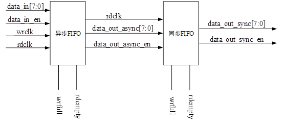
Figure 1. Schematic diagram of the main structure.
The input clock includes two clock frequencies, and this design sets the write clock wrclk to 100MHz and the read clock rdclk to 50MHz when performing the simulation. The read and write of the asynchronous FIFO are controlled by wrclk and rdclk respectively, while the read and write clocks of the synchronous FIFO are both rdclk. Data_in and data_in_en are the input data and enable interface. The data_out_async read from the asynchronous FIFO is used as the input signal for the synchronous FIFO, which is again processed in the first level cache, while the output signal of the synchronous FIFO, data_out_sync, is used directly as the value of the final output signal, data out [6].
4. FIFO verilog design introduction
4.1. Asynchronous FIFO module
The fifo ip core in quartusII is called and instantiated. The FIFO depth is set to 65536 to meet the system's need for a high-capacity asynchronous FIFO, and separate read and write clocks are chosen at the bottom of the clock selection to meet the needs of the asynchronous design. As shown in Figure 2.
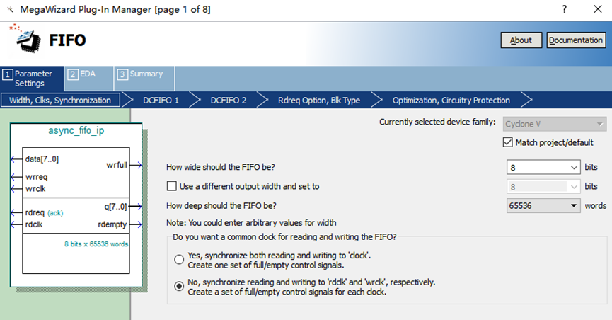
Figure 2. IP core instantiation settings.
4.2. Synchronous FIFO module
The module also calls the corresponding FIFO ip core, except that the clock selection selects the same clock for the read and write clocks. The main structure of the code is a state machine structure. When the input is written, the data is cached into the FIFO and the state machine jumps to the read state, where the input data is read out in turn until the FIFO is empty, and the state machine returns to the initial idle state [7].
4.3. Top-level module and simulation incentive module
The top-level module is mainly used to instantiate the above two FIFO design modules and to interface them accordingly. The simulation excitation module sets rdclk and wrclk to 50MHz and 100MHz respectively, which is used to write test cases, generate excitation data and instantiate the design module for the relevant simulation of the designed functional module code. This simulation generates 1-10 data inputs in turn to test the overall functionality of the code.
5. Simulation verification and analysis
First, after creating a new project in modelsim, add all the above design module verilog code, tb code, and the corresponding. v files for generating the ip cores to the modelsim project. Afterwards, click on compile to compile and check the accuracy of the code. Click on simulate and select tb as the top-level file. Here you need to add the altera_mf_ver wrapper library, which is used to call the ip cores for normal simulation. Finally, add all the module waveforms to the waveform graph, as shown in Fig. 3, which shows the simulated waveform graph for all the signals.
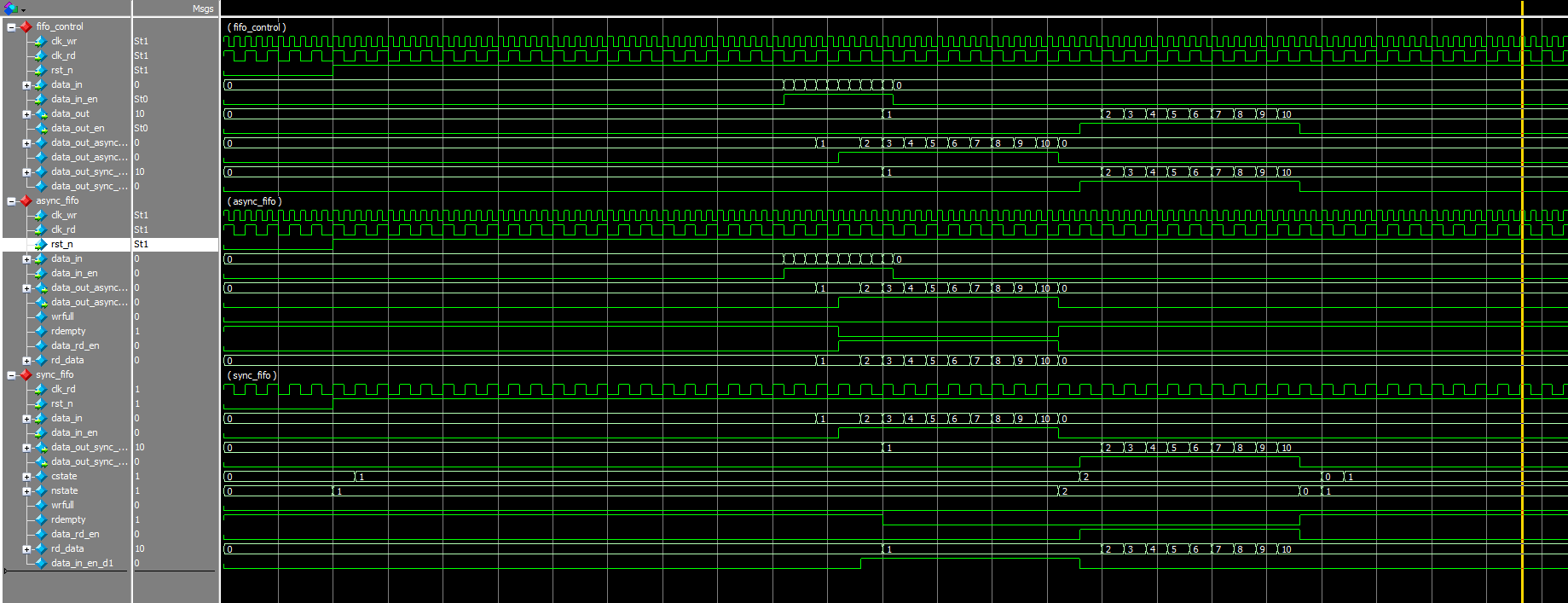
Figure 3. Simulated waveforms of all signals.
As can be seen from Fig.4, the ten data are written to the FIFO in turn and then read out in turn at the clock rate of rdclk, and the asynchronous FIFO emulation functions correctly.
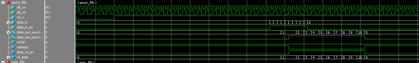
Figure 4. Asynchronous FIFO simulation waveform
From Fig.5, it can be seen that after the data is written to the FIFO sequentially when cstate is in the write state, the data is read out sequentially in the read state, and the data is maintained correctly, and the synchronous FIFO simulation functions correctly.
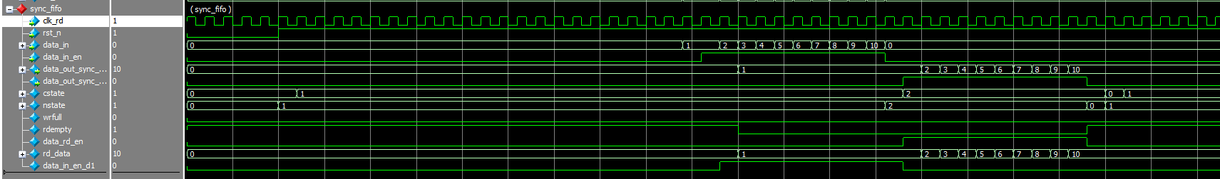
Figure 5. Synchronous FIFO simulation waveform
As can be seen from Fig.6, the initial data entered and the final output data remain the same, the overall simulation function of the code is correct, and the simulation is complete.
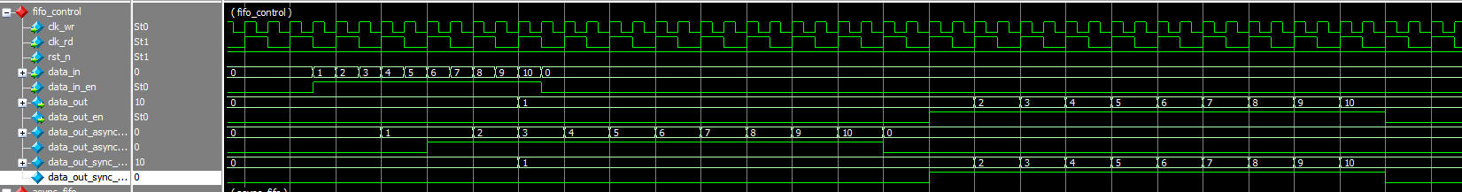
Figure 6. Top-level module simulation waveforms
6. Conclusion
Based on the traditional FIFO architecture, a high-capacity asynchronous FIFO circuit architecture is proposed by cascading asynchronous FIFOs and synchronous FIFOs. The design was carried out in Verilog, and the simulation and verification were based on Modelsim software. The simulation results show that the proposed asynchronous FIFO structure has the advantages of high reliability and large capacity. Based on this paper, the reliability of the data transfer performance of the high-capacity FIFO data cache to the limit can be investigated in the future.
References
[1]. Acharya D, Mehta U S. Performance Analysis of RTL to GDS-II Flow in Opensource Tool Qflow and Commercial Tool Cadence Encounter for Synchronous FIFO[C]//2022 IEEE International Conference of Electron Devices Society Kolkata Chapter (EDKCON). IEEE, 2022: 199-204.
[2]. Kumar P, Moud R. DESIGNING AND VERIFICATION OF ASYNCHRONOUS FIFO[J]. International Journal of Advanced Research in Computer Science, 2022, 13.
[3]. Abasaheb S A, Kamatchi S. Design of Mesochronous Dual Clock Fifo Buffer with Modified Synchronizer Circuit[C]//2022 6th International Conference on Electronics, Communication and Aerospace Technology. IEEE, 2022: 1-7.
[4]. Khosla M. Coverage of Meta-Stability Using Formal Verification in Asynchronous Gray Code FIFO[C]//2022 2nd International Conference on Intelligent Technologies (CONIT). IEEE, 2022: 1-8.
[5]. Khosla M. Coverage of Meta-Stability Using Formal Verification in Asynchronous Gray Code FIFO[C]//2022 2nd International Conference on Intelligent Technologies (CONIT). IEEE, 2022: 1-8.
[6]. Li J, Yang L, Feng X, et al. UART Controller with FIFO Buffer Function Based on APB Bus[C]//2022 IEEE 16th International Conference on Anti-counterfeiting, Security, and Identification (ASID). IEEE, 2022: 1-4.
[7]. de Castro2 Guowei R A L, Yazicigil Y C J R, Joshi A C V V A. FAB: An FPGA-based Accelerator for Bootstrappable Fully Homomorphic Encryption[J].
[8]. Yamamoto K, Fukuhara A, Nishi H. Hardware Implementation of MQTT Broker and Precise Time Synchronization Using IoT Devices[J]. IEEJ Transactions on Electrical and Electronic Engineering, 2022, 17(2): 209-217.
[9]. Hsia S C, Wang S H, Kuo T T. VLSI architecture and implementation of HDR camera signal processor[J]. Journal of Real-Time Image Processing, 2023, 20(1): 6.
[10]. Nowosielski A, Reginia P. Digital Wah-Wah Guitar Effect Controlled by Mouth Movements[C]//Computer Vision and Graphics: Proceedings of the International Conference on Computer Vision and Graphics ICCVG 2022. Cham: Springer Nature Switzerland, 2023: 31-39.
Cite this article
Liu,K. (2023). A verilog design for cascading a large-capacity asynchronous FIFO with a synchronous FIFO. Applied and Computational Engineering,14,25-30.
Data availability
The datasets used and/or analyzed during the current study will be available from the authors upon reasonable request.
Disclaimer/Publisher's Note
The statements, opinions and data contained in all publications are solely those of the individual author(s) and contributor(s) and not of EWA Publishing and/or the editor(s). EWA Publishing and/or the editor(s) disclaim responsibility for any injury to people or property resulting from any ideas, methods, instructions or products referred to in the content.
About volume
Volume title: Proceedings of the 5th International Conference on Computing and Data Science
© 2024 by the author(s). Licensee EWA Publishing, Oxford, UK. This article is an open access article distributed under the terms and
conditions of the Creative Commons Attribution (CC BY) license. Authors who
publish this series agree to the following terms:
1. Authors retain copyright and grant the series right of first publication with the work simultaneously licensed under a Creative Commons
Attribution License that allows others to share the work with an acknowledgment of the work's authorship and initial publication in this
series.
2. Authors are able to enter into separate, additional contractual arrangements for the non-exclusive distribution of the series's published
version of the work (e.g., post it to an institutional repository or publish it in a book), with an acknowledgment of its initial
publication in this series.
3. Authors are permitted and encouraged to post their work online (e.g., in institutional repositories or on their website) prior to and
during the submission process, as it can lead to productive exchanges, as well as earlier and greater citation of published work (See
Open access policy for details).
References
[1]. Acharya D, Mehta U S. Performance Analysis of RTL to GDS-II Flow in Opensource Tool Qflow and Commercial Tool Cadence Encounter for Synchronous FIFO[C]//2022 IEEE International Conference of Electron Devices Society Kolkata Chapter (EDKCON). IEEE, 2022: 199-204.
[2]. Kumar P, Moud R. DESIGNING AND VERIFICATION OF ASYNCHRONOUS FIFO[J]. International Journal of Advanced Research in Computer Science, 2022, 13.
[3]. Abasaheb S A, Kamatchi S. Design of Mesochronous Dual Clock Fifo Buffer with Modified Synchronizer Circuit[C]//2022 6th International Conference on Electronics, Communication and Aerospace Technology. IEEE, 2022: 1-7.
[4]. Khosla M. Coverage of Meta-Stability Using Formal Verification in Asynchronous Gray Code FIFO[C]//2022 2nd International Conference on Intelligent Technologies (CONIT). IEEE, 2022: 1-8.
[5]. Khosla M. Coverage of Meta-Stability Using Formal Verification in Asynchronous Gray Code FIFO[C]//2022 2nd International Conference on Intelligent Technologies (CONIT). IEEE, 2022: 1-8.
[6]. Li J, Yang L, Feng X, et al. UART Controller with FIFO Buffer Function Based on APB Bus[C]//2022 IEEE 16th International Conference on Anti-counterfeiting, Security, and Identification (ASID). IEEE, 2022: 1-4.
[7]. de Castro2 Guowei R A L, Yazicigil Y C J R, Joshi A C V V A. FAB: An FPGA-based Accelerator for Bootstrappable Fully Homomorphic Encryption[J].
[8]. Yamamoto K, Fukuhara A, Nishi H. Hardware Implementation of MQTT Broker and Precise Time Synchronization Using IoT Devices[J]. IEEJ Transactions on Electrical and Electronic Engineering, 2022, 17(2): 209-217.
[9]. Hsia S C, Wang S H, Kuo T T. VLSI architecture and implementation of HDR camera signal processor[J]. Journal of Real-Time Image Processing, 2023, 20(1): 6.
[10]. Nowosielski A, Reginia P. Digital Wah-Wah Guitar Effect Controlled by Mouth Movements[C]//Computer Vision and Graphics: Proceedings of the International Conference on Computer Vision and Graphics ICCVG 2022. Cham: Springer Nature Switzerland, 2023: 31-39.