


1. Introduction
Integrated circuits, due to their high performance, high reliability, high design productivity, low power consumption, and low cost are widely used in all areas of life and production. The demands of today's high-speed data throughput have led to increasing circuit clock frequencies and increasing circuit integration by reducing the feature size of transistors during product development, but the prominent problem of increased power consumption is inevitable. It is therefore a very important area of research today to reduce the power consumption of circuits while maintaining a high level of performance. The flip-flop, a very important component of the integrated circuit, is now used to reduce its power consumption in several ways, including by improving the flip-flop structure, optimizing the clocking scheme, investigating more efficient circuit structures, etc. This paper focuses on some new trigger designs that enhance the trigger structure, such as a reversible flip-flop design with reversible gates, a flip-flop design with memristors, and a sense amplifier-based flip-flop. It describes their logical functions and verifies their low-power characteristics in comparison with conventional flip-flops. It also describes the current state of research on enhancing logic gates to lower flip-flop power consumption.
2. A reversible flip-flop design with reversible gates
Landauer emphasizes that the irreversible operation of current logic circuits is the source of energy consumption. And that the key to reducing power consumption in circuits is to convert irreversible operation to reversible operation [1]. Reversible computing is an important research direction for future low-power integrated circuits because it eliminates energy dissipation due to data loss in traditional logic circuits. Using reversible logic gates to build reversible circuits can effectively reduce computational energy consumption [2].
The main reversible logic gates used in reversible logic networks are NOT gates, Feynman gates, Swap gates, Fredkin gates, and Toffoli gates. In the following design of the reversible flip-flop, the Fredkin gate, the Modified Fredkin gate, and the Feynman gate are mainly used.
Fredkin gates and Modified Fredkin gates are both three input/output gates. Yet their quantum costs are 5 and 4 respectively. This means that if the MF gate can be used instead of the F gate as much as possible, this will significantly reduce energy consumption [3].
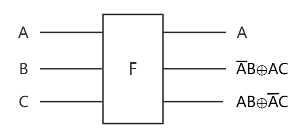
Figure 1. Fredkin gate.
Its function is described as follows: As is shown in Figure 1 that when A is 1, the output of control bit A remains unchanged, and the outputs of target bits B and C are exchanged. When A is 0, neither the control bit A nor the target bits B and C change. When A is 0, neither control bit A nor target bits B and C are changed.
Change the second output of the F gate to \( \overline{A}B⊕A\overline{C} \) , and then the modified fredkin gate (MF gate) can be obtained. Its function is described as follows.: when A is 1, the control bit A is unchanged, the outputs of target bits B and C are swapped, and the target bit C is inverted. When A is 0, both control signal bit A and target bits B and C are unchanged.
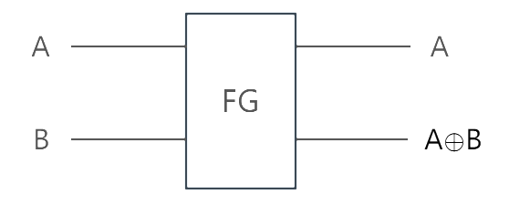
Figure 2. Feynman gate.
Feynman gate is a two input/output gate. Its function is described as follows: As is shown in Figure 2 that when A is 1, the control bit A is output, which is unchanged and the target bit B is inverted; when A is 0, the outputs of both the control and target bits remain unchanged. It can be used to perform inverse and copy operations on signals.
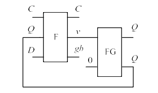
Figure 3. D latch implemented with F gate and FG gate [3].
Figure 3 displays a high-level triggered D latch implemented with an F gate and an FG gate. When C is 0, v = Q, gb = D, in this case, the FG gate copy function enables a loop between the circuit output and the input forming a loop. When C is 1, the F-gate is in the data exchange state, v = D, which causes the output signal of the FG gate to change to D, enabling the update of the data. And a level-triggered reversible D flip-flop with a smaller quantum cost can be obtained by replacing the Fredkin gate with a Modified Fredkin gate with a smaller quantum cost [4].
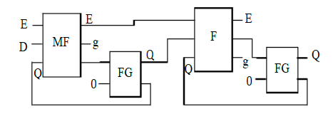
Figure 4. Master-slave D-FF using F, MF and FG gates [4].
Figure 4 shows a master-slave D-FF using F, MF and FG gates. When E = 1, then master FF will work, and when E = 0, slave FF will work. If this research uses the MF gate instead of the F gate, then the quantum cost will be lower. This completes the design of the flip-flop using reversible logic devices.
3. A flip-flop design with memristors
As semiconductor technology advances at a rapid pace, Moore's Law, which was once a great authority, is being challenged [4]. The memristor is the fourth passive basic circuit component with the advantages of low power consumption, non-volatility, and high density. Circuits constructed using memristors can effectively break through bottlenecks, reduce the number of components, and energy consumption, maintain the original efficiency of the circuit. This new device was first proposed in 1971 and created in 2008 [6, 7]. In a bipolar memristor, the resistance of the memristor increases when the current flows in one of the directions, while the resistance increases when the current flows in the opposite direction decreases. Great efforts have been made by previous researchers in the construction of logic circuits using memristors, including material implication [8, 9], memristor-aided logic [10], Reconfigurable non-volatile logic gate circuits [11], and so on. The focus here is to design a D flip-flop based on the reconfigurable non-volatile logic gates [12].
This design was completed using MRL——a hybrid CMOS-memristive logic family [13].In this logic family, the high level (VH) represents logic '1', and the low level (VL) represents logic '0'.
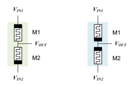
Figure 5. AND gate [12]. Figure 6. OR gate [12].
Figure 5 shows the and gate constructed by MRL,and figure 6 shows the or gate. In the following analysis of the memristor, this study uses ‘M’ to denote its resistance value. Meanwhile, this study takes the example of a logic analysis of and gate. When both inputs are high or both are low, there is no current flow in both memristors and therefore the output level is the same as the output level. And when the input levels of the two inputs are reversed, for example, \( {V_{IN1}} \) inputs at high level and \( {V_{IN2}} \) inputs at low level. When the input levels of the two inputs are reversed, M1 will approach the maximum resistance and M2 will approach the minimum resistance, according to the characteristics of the memristor. The formula below can be adopted to calculate the output voltage.
\( { V_{OUT}}=\frac{M2}{M1+M2}{V_{IN1}} \) (1)
M2 is much smaller than M1, so the value of the output voltage tends to 0. The situation is similar when the inputs of the two memristors are reversed, again outputting 0.
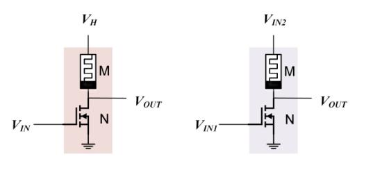
Figure 7. NOT gate and its extension [12].
Figure 7 displays a NOT gate and its extension. Similar to the previous gate, an expression for the output voltage can be easily obtained.
\( { V_{OUT}}=\frac{M}{M+{R_{N}}}{V_{H}} \) (2)
In this expression, \( {R_{N}} \) represents the resistance of that NMOS transistor. When the input goes high, NMOS is on, the output voltage is grounded and it has a value of 0. Conversely, if the input is low, NMOS transistor does not conduct and its resistance tends to infinity. Then \( {V_{OUT}} \) is equal to \( {V_{H}} \) and the output is high. The study can extend this circuit by replacing \( {V_{H}} \) with \( {V_{IN2}} \) to obtain a logical expression like this.
\( { V_{OUT}}=\overline{{V_{IN1}}}*{V_{IN2}} \) (3)
In formula (3), the asterisk (*) represents the 'and' operation.
After introducing these gates, a D flip-flop design can be started. The equation of state for a D flip-flop is as follows(level triggered).
\( {Q_{N+1}}=CD+\overline{C}{Q_{N}} \) (4)
C indicates the clock signal, and D and Q indicate the input and output signals. From the equation of state, it follows that when the clock is at a low level, \( { Q_{N+1}} \) = \( {Q_{N}} \) , the output signal remains constant. Conversely, \( {Q_{N+1}} \) =D. It is important to note that, in the presence of a specific applied current or voltage signal, the resistance of the memristor can be switched between at least two stable resistance states (high and low resistance) and remain constant after the applied electrical signal is removed. Therefore, it is necessary to analyze the situation corresponding to the different outputs of the previous moment. When \( {Q_{N}} \) =1, \( { Q_{N+1}} \) =CD+ \( \overline{C} \) , and when \( {Q_{N}} \) =0, \( {Q_{N+1}}=CD \) . This can be achieved by means of the above-mentioned and gate, or gate and modified not gate.
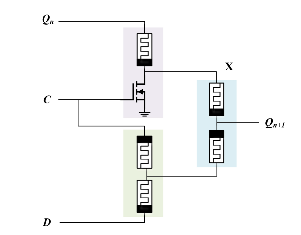
Figure 8. D flip-flop based on MRL [12].
A D flip-flop implemented using memristors is shown in Fig8. When \( {Q_{N}} \) inputs logic 0, X outputs logic 0. Then after passing through the or gate, \( { Q_{N+1}} \) = CD+X = CD can be got. For the same reason, when \( {Q_{N}} \) inputs logic 1, \( { Q_{N+1}} \) =CD+ \( \overline{C} \) can be obtained. So far, a D flip-flop has been designed based on memristor ratioed logic. It can be seen that though the number of devices is the same for a design using a memristor compared to a conventional D flip-flop, the device area is much smaller than a pure CMOS structure. Using a similar approach, this study can also design a JK flip-flop based on the MRL, which can save up to 60.58% of power consumption [12], achieving the goal of designing a low-power flip-flop.
4. Sense amplifier based flip-flop
Flip flops form an important part of the overall circuit design, one of the most effective flip-flops is the Sense Amplifier based Flip-Flop (SAFF) [14]. In the area of high speed and low power performance, a wide range of SAFF designs are preferred by researchers The potential for portable, high computing and low power consumption is very promising. This section focuses on an improved SAFF design from the perspective of the flip-flop’s low power consumption.
Masataka Matsui gives the first design of SAFF, as is shown in Figure 9 [15].
Figure 9. SAFF basic block diagram [15].
The SAFF consists of two parts, a SenseAmplifier (SA) master stage and a slave stage with a reset SR latch.SA) master stage and a slave stage with a reset SR latch. Based on this structure, a restacked adaptive regulation sensitive amplifier and a single-ended output SR latch are proposed [16].
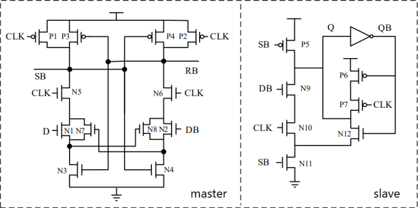
Figure 10. The proposed re-stack adaptive adjustment of single-end output SAFF [16].
Fig.10 displays the proposed re-stack adaptive adjustment of single-end output SAFF. Its function can be divided into three stages.
Stage (1): Input CLK low level, p1 and p2 transistors are turned on, SB and RB precharge VDD high voltage through P1 and P2 transistors, N5 and N6 are turned off. Then N3 and N4 are turned on, N7 and N8 are turned off, and the pre-charging step is completed.
Stage (2): When the rising edge of the clock arrives and makes CLK go high, which results in the cut-off of p1 and p2 while N5 and N6 are on. If D is high, junction SB discharges to low via N5, N1 and N3, simultaneously turning P3 on and N4 off. If D is low, junction RB is discharged low via transistors N6, N2 and N4, simultaneously turning P4 on and N3 off. This completes the induction phase, where a change in D no longer affects the state of junctions SB and RB due to the modulating effect of N7 and N8.
Stage (3): Next, this study analyzes the slave section. If D is high at the rising edge of the clock, SB discharge goes low, as seen in stage 2, causing P5 to conduct and N9, N10, and N11 to cut off. At this point, Q goes high. If D is low on the rising edge of the clock, SB remains high and P5 turns off while N9, N10, N11 conduct, at which point Q is grounded and goes low. When the clock is low, as can be seen from stage 1, SB and RB are held high, the P5, P9, and N10 transistors are cut off, and the Q and QB signals are latched.
At this point, this research has completed the design of re-stack adaptive adjustment of single-end output SAFF. Conventional sense amplifier based flip-flop (Con SAFF) is one of the most efficient low-power flip-flops available [17]. The new SAFF offers an average power saving of 26% compared to the Con SAFF, including a 32% saving at α (switching activity) = 12.5%, a 46% reduction in clock-to-output latency, and an average reduction of approximately 3 times in power delay product for different process angles and different input data switching frequencies [16].
5. Conclusion
In several of the flip-flops described in this article, flip-flops based on reversible logic gate construction, replacing F gates with MF gates, can effectively reduce the quantum cost and reduce energy consumption. The flip-flop constructed using a memristor has been proven to consume significantly less energy than conventional flip-flops and occupies a smaller area in the chip, SAFF has a short set-up time and hold time, which greatly reduces its clock load. All three of these flip flops use new devices to achieve what traditional CMOS flip flops do. but unfortunately, it is difficult to make a side-by-side comparison of energy consumption because the fields are different. There are many ways to reduce the power consumption of flip-flops, and in the future, efforts can be made to combine new flip-flops with optimized clock technology and improved semiconductor processes to design low-power, high-performance large-scale integrated circuits.
References
[1]. R. Landauer, "Irreversibility and Heat Generation in the Computing Process," in IBM Journal of Research and Development, vol. 5, no. 3, pp. 183-191, July 1961, doi: 10.1147/rd.53.0183.
[2]. C. H. Bennett, "Logical Reversibility of Computation," in IBM Journal of Research and Development, vol. 17, no. 6, pp. 525-532, Nov. 1973, doi: 10.1147/rd.176.0525.
[3]. ZHANG Ying; WANG Lun-yao; XIA Yin-shui. Design of reversible double-edge flip-flops[J].Journal of Ningbo University(Natural Science & Engineering Edition), 2018, 31(5): 45-50. DOI:10.3969/j.issn.1001-5132.2018.05.009.P.L. Singh, A. Majumder, B. Chowdhury, A.J. Mondal, T.S. Shekhawat,
[4]. Singh P L, Majumder A, Chowdhury B, et al. Reducing delay and quantum cost in the novel design of reversible memory elements[J]. Procedia Computer Science, 2015, 57:189-198.
[5]. PANG Jian; LIU Jia.Review of the Moore’s Law Development[J]. Science and Technology Management Research, 2015, 35(15): 46-50.
[6]. L. Chua, "Memristor-The missing circuit element," in IEEE Transactions on Circuit Theory, vol. 18, no. 5, pp. 507-519, September 1971, doi:10.1109/TCT.1971.1083337.
[7]. Strukov, D., Snider, G., Stewart, D. et al. The missing memristor found. Nature 453, 80–83 (2008).
[8]. Borghetti J, Snider GS, Kuekes PJ, Yang JJ, Stewart DR, Williams RS. 'Memristive' switches enable 'stateful' logic operations via material implication. Nature. 2010 Apr 8;464(7290):873-6. doi: 10.1038/nature08940. PMID: 20376145.
[9]. Guckert L, Swartzlander E E. MAD gates—Memristor logic design using driver circuitry [J]. IEEE Transactions on Circuits and Systems II: Express Briefs, 2016, 64(2): 171-175.
[10]. Thangkhiew P L, Gharpinde R, Datta K. Efficient mapping of Boolean functions to memristor crossbar using MAGIC NOR gates[J]. IEEE Transactions on Circuits and Systems I: Regular Papers, 2018, 65(8): 2466-2476.
[11]. Hu S Y, Li Y, Cheng L, et al. Reconfigurable Boolean logic in memristive crossbar: the principle and implementation[J]. IEEE Electron Device Letters, 2018, 40(2): 200-203.
[12]. Wang Ziling. Memristor-based Circuit Design for Logic Gates and Flip-Flops[D]. Southwest University, 2022. DOI:10.27684/d.cnki.gxndx.2022.000800.
[13]. S. Kvatinsky, N. Wald, G. Satat, A. Kolodny, U. C. Weiser and E. G. Friedman, "MRL — Memristor Ratioed Logic," 2012 13th International Workshop on Cellular Nanosc-ale Networks and their Applications, Turin, Italy, 2012, pp. 1-6, doi: 10.1109/CNNA.2012.6331426.
[14]. HUANG Zhengfeng; SU Zian; CAO Di; QI Haochen; NI Tianming; XU Qi. A high—performance, low—power flip—flop design based on sense amplifier[J]. Journal of Hefei University of Technology (Natural Science), 2020, 43(12): 1633-1638.
[15]. M. Matsui et al., "A 200 MHz 13 mm/sup 2/ 2-D DCT macrocell using sense-amplifying pipeline flip-flop scheme," in IEEE Journal of Solid-State Circuits, vol. 29, no. 12, pp. 1482-1490, Dec. 1994, doi: 10.1109/4.340421.
[16]. GONG Qi Fan. A Low Power Design of Sense Amplifier Flip Flop[D]. Anhui: Anhui University, 2022.
[17]. Montanaro, J.; Witek, R.T..A 160-MHz, 32-b, 0.5-W CMOS RISC microprocessor[J]. Solid-State Circuits, IEEE Journal of, 1996, Vol.31(11): 1703-1714.
Cite this article
Luo,Y. (2023). Review of innovations in low-power flip-flops based on the development of innovative logic gates. Applied and Computational Engineering,23,52-58.
Data availability
The datasets used and/or analyzed during the current study will be available from the authors upon reasonable request.
Disclaimer/Publisher's Note
The statements, opinions and data contained in all publications are solely those of the individual author(s) and contributor(s) and not of EWA Publishing and/or the editor(s). EWA Publishing and/or the editor(s) disclaim responsibility for any injury to people or property resulting from any ideas, methods, instructions or products referred to in the content.
About volume
Volume title: Proceedings of the 2023 International Conference on Functional Materials and Civil Engineering
© 2024 by the author(s). Licensee EWA Publishing, Oxford, UK. This article is an open access article distributed under the terms and
conditions of the Creative Commons Attribution (CC BY) license. Authors who
publish this series agree to the following terms:
1. Authors retain copyright and grant the series right of first publication with the work simultaneously licensed under a Creative Commons
Attribution License that allows others to share the work with an acknowledgment of the work's authorship and initial publication in this
series.
2. Authors are able to enter into separate, additional contractual arrangements for the non-exclusive distribution of the series's published
version of the work (e.g., post it to an institutional repository or publish it in a book), with an acknowledgment of its initial
publication in this series.
3. Authors are permitted and encouraged to post their work online (e.g., in institutional repositories or on their website) prior to and
during the submission process, as it can lead to productive exchanges, as well as earlier and greater citation of published work (See
Open access policy for details).
References
[1]. R. Landauer, "Irreversibility and Heat Generation in the Computing Process," in IBM Journal of Research and Development, vol. 5, no. 3, pp. 183-191, July 1961, doi: 10.1147/rd.53.0183.
[2]. C. H. Bennett, "Logical Reversibility of Computation," in IBM Journal of Research and Development, vol. 17, no. 6, pp. 525-532, Nov. 1973, doi: 10.1147/rd.176.0525.
[3]. ZHANG Ying; WANG Lun-yao; XIA Yin-shui. Design of reversible double-edge flip-flops[J].Journal of Ningbo University(Natural Science & Engineering Edition), 2018, 31(5): 45-50. DOI:10.3969/j.issn.1001-5132.2018.05.009.P.L. Singh, A. Majumder, B. Chowdhury, A.J. Mondal, T.S. Shekhawat,
[4]. Singh P L, Majumder A, Chowdhury B, et al. Reducing delay and quantum cost in the novel design of reversible memory elements[J]. Procedia Computer Science, 2015, 57:189-198.
[5]. PANG Jian; LIU Jia.Review of the Moore’s Law Development[J]. Science and Technology Management Research, 2015, 35(15): 46-50.
[6]. L. Chua, "Memristor-The missing circuit element," in IEEE Transactions on Circuit Theory, vol. 18, no. 5, pp. 507-519, September 1971, doi:10.1109/TCT.1971.1083337.
[7]. Strukov, D., Snider, G., Stewart, D. et al. The missing memristor found. Nature 453, 80–83 (2008).
[8]. Borghetti J, Snider GS, Kuekes PJ, Yang JJ, Stewart DR, Williams RS. 'Memristive' switches enable 'stateful' logic operations via material implication. Nature. 2010 Apr 8;464(7290):873-6. doi: 10.1038/nature08940. PMID: 20376145.
[9]. Guckert L, Swartzlander E E. MAD gates—Memristor logic design using driver circuitry [J]. IEEE Transactions on Circuits and Systems II: Express Briefs, 2016, 64(2): 171-175.
[10]. Thangkhiew P L, Gharpinde R, Datta K. Efficient mapping of Boolean functions to memristor crossbar using MAGIC NOR gates[J]. IEEE Transactions on Circuits and Systems I: Regular Papers, 2018, 65(8): 2466-2476.
[11]. Hu S Y, Li Y, Cheng L, et al. Reconfigurable Boolean logic in memristive crossbar: the principle and implementation[J]. IEEE Electron Device Letters, 2018, 40(2): 200-203.
[12]. Wang Ziling. Memristor-based Circuit Design for Logic Gates and Flip-Flops[D]. Southwest University, 2022. DOI:10.27684/d.cnki.gxndx.2022.000800.
[13]. S. Kvatinsky, N. Wald, G. Satat, A. Kolodny, U. C. Weiser and E. G. Friedman, "MRL — Memristor Ratioed Logic," 2012 13th International Workshop on Cellular Nanosc-ale Networks and their Applications, Turin, Italy, 2012, pp. 1-6, doi: 10.1109/CNNA.2012.6331426.
[14]. HUANG Zhengfeng; SU Zian; CAO Di; QI Haochen; NI Tianming; XU Qi. A high—performance, low—power flip—flop design based on sense amplifier[J]. Journal of Hefei University of Technology (Natural Science), 2020, 43(12): 1633-1638.
[15]. M. Matsui et al., "A 200 MHz 13 mm/sup 2/ 2-D DCT macrocell using sense-amplifying pipeline flip-flop scheme," in IEEE Journal of Solid-State Circuits, vol. 29, no. 12, pp. 1482-1490, Dec. 1994, doi: 10.1109/4.340421.
[16]. GONG Qi Fan. A Low Power Design of Sense Amplifier Flip Flop[D]. Anhui: Anhui University, 2022.
[17]. Montanaro, J.; Witek, R.T..A 160-MHz, 32-b, 0.5-W CMOS RISC microprocessor[J]. Solid-State Circuits, IEEE Journal of, 1996, Vol.31(11): 1703-1714.