


1. Introduction
The growth of the power electronics business has been significantly influenced by semiconductor technology [1]. Power semiconductor devices have historically been regarded as a crucial part of power electronic equipment. Power silicon devices have a well-established field of use, but as industry demand has increased, silicon devices' physical restrictions have caused them to become less suitable for a variety of applications requiring high power density, high efficiency, high temperature, and high voltage. SiC materials are a very desirable candidate for applications requiring high power and high temperature [2, 3]. Because SiC MOSFET have substantially lower on-resistance and switching losses than Si MOSFET with identical power levels, they are suited for higher operating frequencies.
SiC MOSFETs have long employed silicon dioxide as the gate dielectric layer, although this material has drawbacks as well [4]. Especially, two issues come up. SiO2 can create a 2.5 times greater electric field than SiC because it has a lower dielectric constant by 2.5 times. Moreover, the SiO2 and SiC contact has a high density of surface traps. To overcome this, the likely low-SiO2 materials should be replaced by high-dielectric materials as the alternate gate oxide, such as HfO2, Al2O3, HfSION, ZrO2, Ta2O5, La2O3, LaLuO3, NiO, TiO2, CeO2, GaF2, AlN, Si3N4, etc.
This article will introduce several main emerging high-k dielectric layer materials, and compare and analyze the influence of dielectric layers of different materials on SiC MOSFET characteristics.
2. SiC MOSFET and its gate dielectrics
2.1. SiC MOSFETs
The new SiC material has drawn a lot of interest since it has better physical characteristics than Si material [5]. The energy needed to attract electrons from a material's valence band to its conduction band is known as the bandgap. The band gap of Si is 1.1 eV, while that of SiC is 3.26 eV. SiC devices perform better in terms of electric field breakdown than Si because of the higher energy needed for electrons to migrate to the conduction band. For the same drift area thickness, SiC devices have a greater blocking voltage because their critical breakdown electric fields are roughly ten times larger than those of silicon. As a result, for devices with the same blocking voltage, a greater critical breakdown electric field allows for a reduction in the thickness of the lightly doped drift zone, as well as a reduction in the drift region's resistance and conduction loss in the SIC device. SiC devices are appropriate for high switching frequency applications because the saturation drift speed of the material is twice as fast as that of Si. Moreover, the release of stored charge from the diode's depletion zone can proceed more quickly due to the increased saturation drift speed. SiC diodes have reduced reverse recovery loss and a faster reverse recovery time as a result. Finally, SiC materials have a thermal conductivity that is around three times that of Si. High thermal conductivity allows for more power to be generated inside the semiconductor material while also making system cooling components (such as heat sinks and fans) simpler to use, which lowers system cost and volume.
Since its birth, SiC MOSFET has drawn a lot of attention in the field of power electronics due to its great performance [6]. Compared to silicon-based MOSFETs, SiC MOSFETs are better suited for applications that have voltage, frequency, temperature, and density of very high values. SiC MOSFET offers the clearest high-temperature properties when compared to other power electronic devices. The thermal breakdown junction temperature of SiC MOSFETs can reach 300 degrees Celsius, which is higher than that of conventional silicon-based MOSFETs, which only reach 170 degrees Celsius. The development of SiC MOSFET has significantly increased the efficiency of power electronic devices by allowing them to operate in high-demand conditions settings. Simultaneously, power electronic devices’ volume is lowered and the advancement of power electronic devices toward miniaturization and high efficiency is encouraged due to SiC MOSFETs' lower loss. SiC MOSFET applications are gradually becoming larger and larger. Compared with traditional silicon device applications, the use of silicon carbide power devices has higher operating efficiency, lower loss, and smaller volume. It can be better applied to high voltage and high power fields such as smart grids, solar photovoltaic power generation, electric traction, new energy electric vehicles, and industrial motors.
2.2. Gate dielectrics of SiC MOSFETs
Between the transistor's channel region and the MOSFET's gate electrode, there is a layer of insulation called the gate dielectric [2]. In use, an electric field is produced by the voltage at the gate in the channel area, which stops current flow. But in recent decades, as silicon transistors have shrunk in size, insulating layers made of silicon dioxide have had to get thinner and thinner to control current with less voltage, reducing energy consumption. Eventually, the insulating barrier becomes so thin that electric charges can pass through it, causing current to leak and waste energy. So various new gate dielectric layer materials began to appear, the most typical ones are high-κ dielectrics (HfO2, Al2O3, HfSION, ZrO2, Ta2O5, TiO2, CeO2, etc.) However, various high performance of -k dielectrics is also different. Al2O3 is drawing the most attention as a potential SiO2 replacement among them because of its superior lattice matching to SiC, compatibility with 4H-SiC, high-k value, strong thermal stability, a fairly wide dielectric bandgap, and a conduction band offset that is not excessively high. The high k value of HfO2 makes it appear as another intriguing possibility for 4H-SiC MOS devices. Zirconia (ZrO2), which is nearly identical to HfO2, has a dielectric constant close to 25 and its bandgap is about 5.8–7.8 eV, and it also has excellent thermal stability when near the Si substrate [7]. Because of its high refractive index, chemical and thermal resilience, high dielectric constant, compatibility with microelectronics operations, and high refractive index, Ta2O5 has already drawn considerable interest as the gate dielectric for high-density memory cells and MOS field-effect transistors [8]. Then, for TiO2, even if its electrical bandgap is very tiny (3.5 eV), it is nevertheless possible to change its dielectric constant from 40 to 110, which has a significant impact on the ability to start MOSFET [9]. Moreover, CeO2 has a broad bandgap, a low interface state density, a high dielectric constant, and strong thermal stability. It has been used as a gate insulator and storage capacitor in many applications. [10]. The extraordinarily high (40) dielectric constant of metal oxides like HfO2 makes them appealing, but they also have drawbacks including lower mobility and unstable threshold voltage brought on by charge trapping [11]. The use of silicates, which have substantially lower threshold voltage fluctuations than silicon-based media and form a more stable interface with silicon, is one possible solution. Among silicate materials, HfSION is a relatively ideal silicate for use as a grid dielectric.
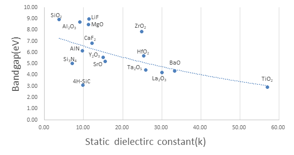
Figure 1. The bandgap of different static dielectric constant.
Figure 1 shows the bandgap of different static dielectric constant, it visually shows the bandgap corresponding to a different gate dielectric.
The following section of this article will concentrate on these three gate dielectrics (Al2O3, HfO2, and HfSION), examine how they affect MOSFET performance, and then compare and contrast the three.
3. Al2O3 as gate dielectric layer
3.1. Al2O3 material properties and general behavior as a dielectric layer
In-depth research into Aluminum oxide (Al2O3) for use as a possible gate oxide in SiC MOS technology. has recently been conducted [12]. Al2O3 has a broad bandgap of about 7.0 eV, which is its primary benefit as a gate dielectric. It is anticipated that the 1.6 eV Al2O3 conduction band offset to 4H-SiC will be adequate for n-channel MOSFET functioning. Alumina (Al2O3) has been thoroughly researched for numerous uses and is a very stable and durable material. Al2O3 has numerous advantageous characteristics that make it useful as a substitute gate dielectric, the capacity to become amorphous under the desired circumstances, a high bandgap, and the thermodynamic stability of Si at high temperatures. The disadvantage is that Al2O3 only possesses k8–10, which limits its applicability as a long-term solution for industry (1-2 generations) [13].
3.2. Performance evaluation of Al2O3 dielectric layer SiC MOSFETs
According to research on MOS structures using 4H-SiC produced by sublimation and gate dielectrics of Al2O3 and SiO2 [14], both the dielectric and the substrate type have a significant impact on the types of charges that affect the electrochemical characteristics of the samples.
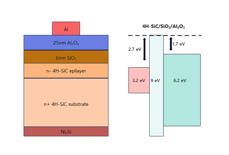
Figure 2. Diagram of the band alignment and cross-section of a schematic MOSFETS capacitor for an Al2O3, SiO2, and 4H-SiC system.
Figure 2 shows the structure of 4H-SiC MOS with Al2O3 as the main gate dielectric and it also shows the band alignment in Al2O3, SiO2, and 4H-SiC system. The structure shows the width of the main gate dielectric and the position of Al2O3 , it is halfway between Al and SiO2. 4H-SiC is 2.7eV from SiO2 while Al2O3 is 1.7eV from SiO2 from the band diagram in the system.
The n-type 4H-SiC/SiO2 structures display exceptional performance on the C-V curves with a low density of interface states and net oxide charge. The findings show that donor-type slow phases, which greatly increase C-V curve hysteresis in severe depletion, are the principal sources of weakness in these systems. Al2O3 on n-type SiC exhibits a sizable quantity of interface, slow, and positive net charges in the samples. The slow states in this scenario are acceptor type and cause hysteresis in depletion, in contrast to SiO2 structures. Considering how these conditions affect the mobility of the carrier channel, this distinction may be crucial. In comparison to samples with SiO2 deposits, samples with Al2O3 deposits on p-type 4H-SiC exhibit better C-V characteristics. For 4H-SiC-MOSFETs with Al2O3 gate insulators made at low temperatures via metal-organic chemical vapor deposition, ultrahigh channel mobility has been observed [15].
4. HfO2 as gate dielectric layer
4.1. HfO2 material properties and general behavior as a dielectric layer
High-K material HfO2 fits the gate's requirements by having a substantial offset from silicon's conduction band (>l eV), a broadband gap (5.7 eV), and a large dielectric constant (25) [16,17]. One of the most promising substitutes for SiO2 at the moment is HfO2, which is gradually being employed in modern integrated circuits. Because of HfO2's high dielectric constant, which reduces the channel-to-gate direct tunnel current, the gate width can be raised while still exerting the same control over the channel. HfO2 has taken the position of SiO2 as the favored high-K dielectric material due to its steady thermodynamic characteristics on silicon. The gate's corresponding oxide layer thickness can be kept constant in this way, and the initial working performance can be preserved. In addition, the tunneling current of the gate can be effectively reduced, and the control ability of the gate under high electric field strength can be improved.
4.2. Performance evaluation of HfO2 dielectric layer SiC MOSFETs
Although having a higher dielectric constant than SiO2, HfO2 has a narrower bandgap, which leads to reduced conduction band offsets for SiC materials [2].
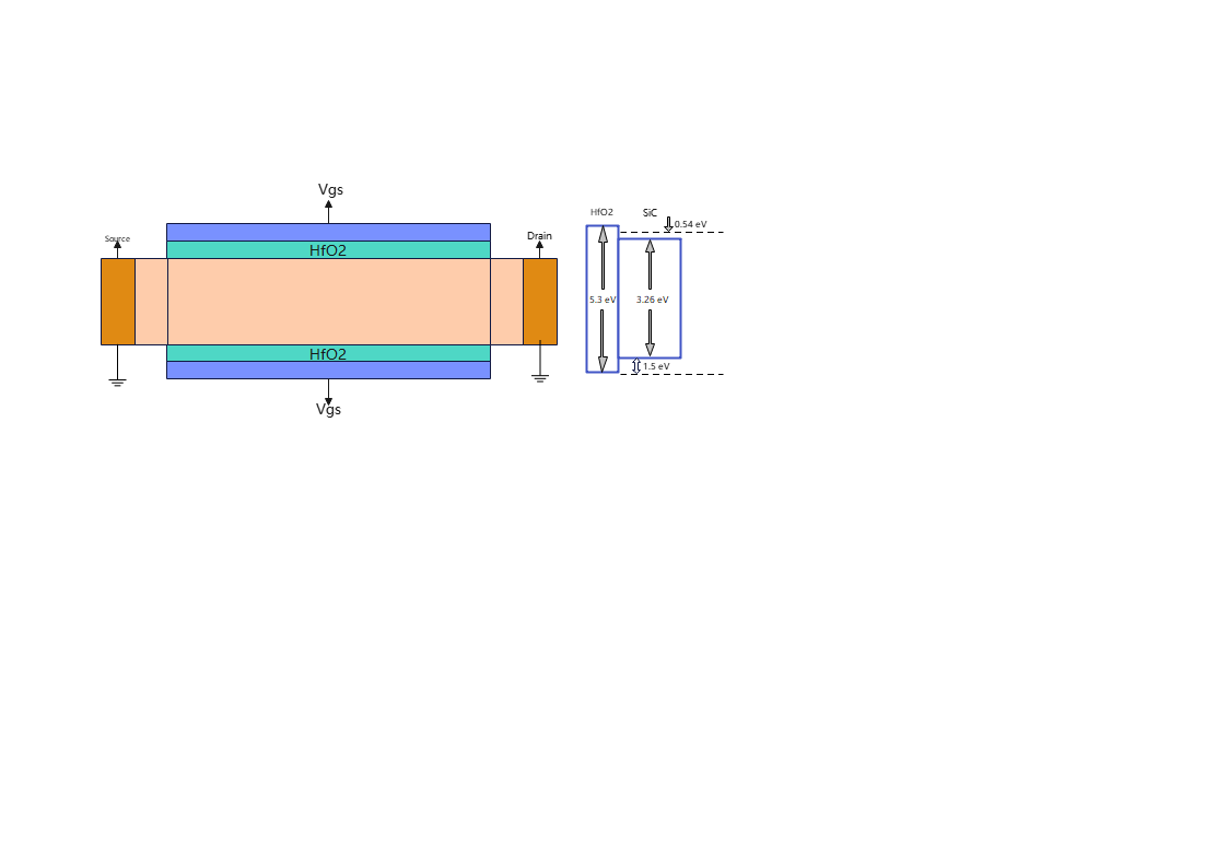
Figure 3. Structure diagram of HfO2 as gate dielectric in MOSFETS and the schematic band alignments for HfO2/SiC system.
Figure 3 shows the structure diagram of HfO2 as gate dielectric in MOSFETS and the schematic band alignments for HfO2/SiC system. In this system, HfO2 alone acts as the gate material to start the MOSFET. It can be seen from the band diagram that the bandgap of HfO2 is higher than that of SiC.
Carrier tunnelling through into the dielectric is far more likely at very low conduction band offset levels, which may restrict the uses of this high-k material. Little conduction band offset and enhanced surface trap density at the HfO2/SiC interface have been found to cause significant leakage current densities, which may affect the MOSFET's electron transport characteristics. The dielectric constant of HfO2 is very high so it makes a good gate oxide for Si-MOSFETs in low-power devices. Yet, the 5.7 eV low bandgap value of 4H-SiC-based MOSFET makes them seem prohibitively expensive. The increased dielectric constant values of the dielectric material result in a substantial decrease in the electric field. The narrow band offsets at the dielectric/SiC interface for SiC-based MOS devices have recently been resolved by the addition of an ultrathin SiO2 interface layer between SiC and high-k HfO2 dielectrics.
5. HfSION as gate dielectric layer
5.1. HfSION material properties and general behavior as a dielectric layer
The extraordinarily high (40) dielectric constant of metal oxides like HfO2 makes them desirable, but they also have drawbacks including lower mobility and unstable threshold voltage brought on by charge trapping [18]. Due to their more stable silicon interface and significantly lower threshold voltage instability, silicates are a potential partial replacement for Si-based dielectrics. The drawback is those metal oxides, often known as "mid-k" dielectric materials, have a substantially greater dielectric constant than silicate. Although the dielectric constant of the hafnium silicate layers utilized in this work, 11, is only three times that of SiO2, it is believed that this will allow for the construction of layers that are thick enough to address the leakage current issue.
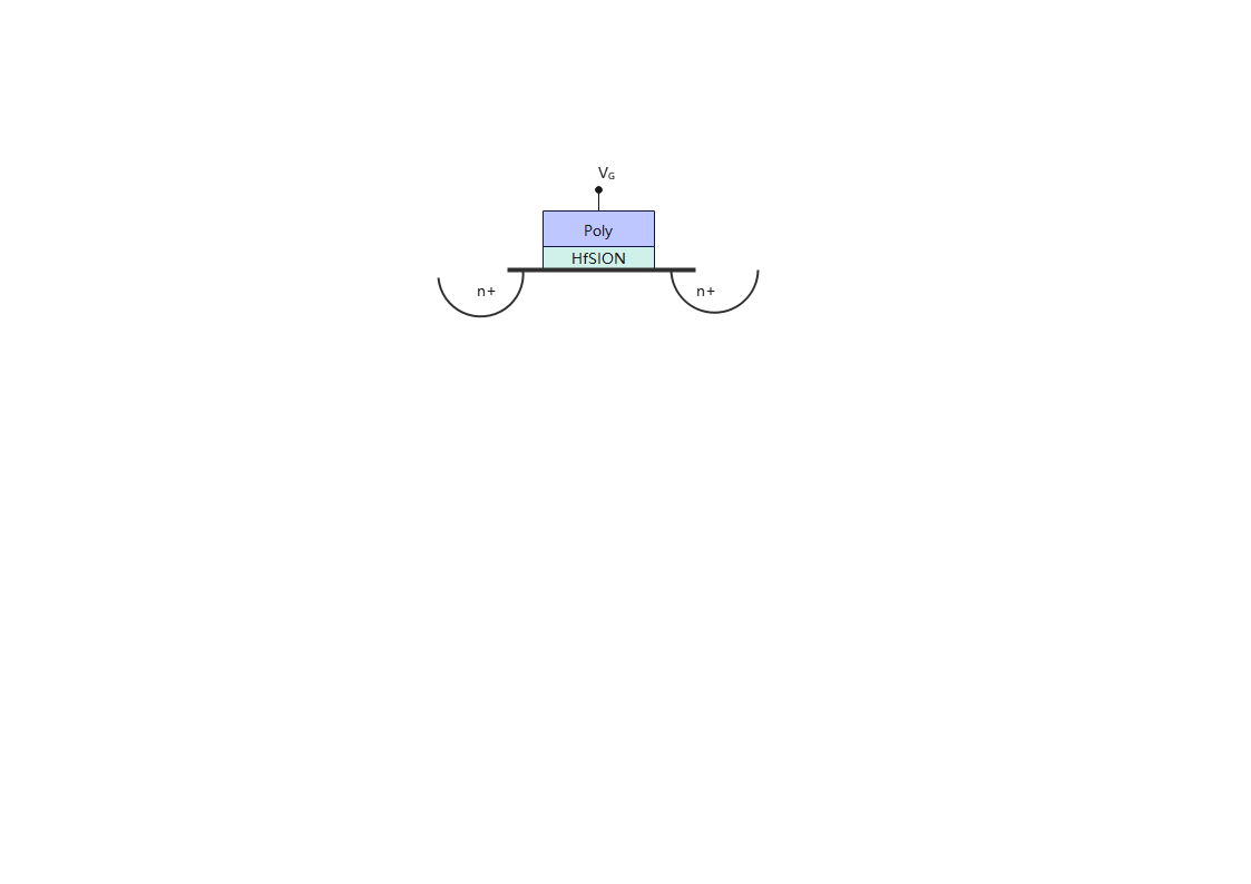
Figure 4. Structure diagram of HfSION as gate dielectric MOSFETS.
Figure 4 shows the structure of HfSION as gate dielectric MOSFETS. HfSION alone acts as the gate dielectric material, and its thickness is larger to reduce leakage current.
5.2. Performance evaluation of HfSiON dielectric layer SiC MOSFETs
Low leakage current compared to SO2, low specific trap density, electron, and hole carrier mobilities at 80% of the universal curve at Eff > 0.8 MV/cm, and low interfacial trap density are just a few of HfSiON's superior electrical characteristics. It can also adapt to an equivalent oxide layer thickness of less than 10A. Additionally, this substance is significantly more effective in blocking boron than SiO2 and SiON when in contact with polysilicon, and it is thermally stable up to 1100 °C [19]. HfSiON gate dielectrics subjected to positive biased temperature stress revealed charge trapping rates that were satisfactory and met reliability standards [20]. For ten years, HfSiON gate dielectrics can be safely used at 1.2 V at 105 °C without significantly changing the threshold voltage or driving current. In contrast to conventional SiO2-based dielectrics, charge trapping in HfSiON exhibits a logarithmic trend over time. HfSiON is a viable choice for high-k gate dielectrics since it demonstrates good material and electrical attributes in addition to appropriate electrical stability.
6. Evaluation and comparison of these three gate dielectrics
High dielectric constant materials include Al2O3 and HfO2. Both materials were successful in reducing the gate's tunneling current and enhancing gate control in high electric fields. HFO2 and SiC materials have highly different band gaps and the narrower band gap of HFO2 results in less conduction band migration than SiC materials [2]. The use of such high k materials may be constrained by the fact that carriers are substantially more likely to pass through the dielectric with very low band offsets. However, Al2O3 has a larger band gap and a conduction band offset of around 1.6 eV than 4H-SiC, which are projected to be sufficient for N-channel MOSFET operation. Al2O3 has superior properties over HfO2 in this comparison. Because of their extraordinarily high permittivity, metal oxides (such as HfO2 and Al2O3) are suitable, but they also have charge capture, reduced mobility, and threshold voltage instability issues. Silicate and silicon forms are an option that can be utilized as a partial replacement for silicon-based dielectrics since they have substantially lower threshold voltage instability and can build a more stable interface. Silicate HfSION will enable the creation of layers thick enough to address leakage current issues because its dielectric constant is substantially lower than that of metal oxides. HfSiON thus outperforms HfO2 and Al2O3 in this regard.
7. Conclusion
This paper focuses on the analysis and detailed introduction of the characteristics of three gate dielectrics and their application in SiC MOSFET analyzes the effects of different gate dielectrics on SiC MOSFET and obtains their advantages and disadvantages. Finally, compare and analyze the three materials, and discuss their respective advantages and disadvantages.
References
[1]. Lu, Y.J. (2013) .Tanhuagui MOSFET yingyong jishu yanjiu[Research on Application technology of SIC MOSFET]. Nanjing hangkonghangtian daxue.
[2]. Nawaz, M. (2015). Research Article On the Evaluation of Gate Dielectrics for 4H-SiC Based Power MOSFETs.
[3]. Sun,K., Lu,Y.J., Wu,H.F., Xing,Y., Huang,L.P.(2013) .Tanhuagui MOSFET de bianwudu canshu moxing [Modeling of variable temperature parameters of silicon carbide MOSFET]. Zhongguo dianji gongcheng xuebao.
[4]. Taube, A., Gierałtowska, S., Gutt, T., Małachowski, T., Pasternak, I., Wojciechowski, T., ... & Piotrowska, A. (2011). Electronic Properties of Thin HfO _2 Films Fabricated by Atomic Layer Deposition on 4H-SiC. Acta Physica Polonica A, 119(5), 696-698.
[5]. Jiang, X. (2021). Tanhuagui MOSFET jianguxing yu kekaoxing yanjiu [Study on robustness and Reliability of SiC MOSFET]. Hunan daxue.
[6]. Li, X.X. (2016). SiC MOSFET yanjiu ji yingyong [Research and application of SiC MOSFET]. Beijing jiaotong daxue.
[7]. Xie, J., Zhu, Z., Tao, H., Zhou, S., Liang, Z., Li, Z., ... & Peng, J. (2020). Research progress of high dielectric constant zirconia-based materials for gate dielectric application. Coatings, 10(7), 698.
[8]. Bartic, C., Jansen, H., Campitelli, A., & Borghs, S. (2002). Ta2O5 as gate dielectric material for low-voltage organic thin-film transistors. Organic electronics, 3(2), 65-72.
[9]. Albertin, K. F., Valle, M. A., & Pereyra, I. (2007). Study of MOS capacitors with TiO2 and SiO2/TiO2 gate dielectric. Journal of Integrated Circuits and Systems, 2(2), 89-93.
[10]. Yoo, J. H., Nam, S. W., Kang, S. K., Jeong, Y. H., Ko, D. H., Ku, J. H., & Lee, H. J. (2001). A study on the microstructure and electrical properties of CeO2 thin films for gate dielectric applications. Microelectronic engineering, 56(1-2), 187-190.
[11]. O'Connor, R., Hughes, G., Degraeve, R., Kaczer, B., & Kauerauf, T. (2004). Reliability of HfSiON gate dielectrics. Semiconductor science and technology, 20(1), 68.
[12]. Khosa, R. Y. (2017). Electrical characterization of gate dielectrics for 4H-SiC MOSFETs.
[13]. Wilk, G. D., Wallace, R. M., & Anthony, J. (2001). High-κ gate dielectrics: Current status and materials properties considerations. Journal of applied physics, 89(10), 5243-5275.
[14]. Paskaleva, A., Ciechonski, R. R., Syväjärvi, M., Atanassova, E., & Yakimova, R. (2005). Characterization of 4H-SiC MOS structures with Al2O3 as gate dielectric. In Materials Science Forum (Vol. 483, pp. 709-712). Trans Tech Publications Ltd.
[15]. Hino, S., Hatayama, T., Kato, J., Tokumitsu, E., Miura, N., & Oomori, T. (2008). High channel mobility 4 H-Si C metal-oxide-semiconductor field-effect transistor with low temperature metal-organic chemical-vapor deposition grown Al2O3 gate insulator. Applied Physics Letters, 92(18), 183503.
[16]. Wei, Q.X. (2011). HfO_2 gaojiedianchangshu shanjiezhibomo de zhibei jiqi dianxuexingneng de yanjiu [Preparation and electrical properties of HfO_2 high dielectric constant grid dielectric films]. Hubei daxue.
[17]. Shi, L. N. ,(2014). Gao κ-weishan MOSFET qijian de shanji suichuandianliu yanjiu[Study on gate tunneling current of high κ-enclosing gate MOSFET devices]. Xian dianzikeji daxue.
[18]. O'Connor, R., Hughes, G., Degraeve, R., Kaczer, B., & Kauerauf, T. (2004). Reliability of HfSiON gate dielectrics. Semiconductor science and technology, 20(1), 68.
[19]. Rotondaro, A. L. P., Visokay, M. R., Chambers, J. J., Shanware, A., Khamankar, R., Bu, H., ... & Colombo, L. (2002, June). Advanced CMOS transistors with a novel HfSiON gate dielectric. In 2002 Symposium on VLSI Technology. Digest of Technical Papers (Cat. No. 01CH37303) (pp. 148-149). IEEE.
[20]. Shanware, A., Visokay, M. R., Chambers, J. J., Rotondaro, A. L. P., Bu, H., Bevan, M. J., ... & Colombo, L. (2003, March). Evaluation of the positive biased temperature stress stability in HfSiON gate dielectrics. In 2003 IEEE International Reliability Physics Symposium Proceedings, 2003. 41st Annual. (pp. 208-213). IEEE.
Cite this article
Sun,Z. (2023). Comparison and analysis of gate dielectrics for SiC MOSFET. Applied and Computational Engineering,23,223-229.
Data availability
The datasets used and/or analyzed during the current study will be available from the authors upon reasonable request.
Disclaimer/Publisher's Note
The statements, opinions and data contained in all publications are solely those of the individual author(s) and contributor(s) and not of EWA Publishing and/or the editor(s). EWA Publishing and/or the editor(s) disclaim responsibility for any injury to people or property resulting from any ideas, methods, instructions or products referred to in the content.
About volume
Volume title: Proceedings of the 2023 International Conference on Functional Materials and Civil Engineering
© 2024 by the author(s). Licensee EWA Publishing, Oxford, UK. This article is an open access article distributed under the terms and
conditions of the Creative Commons Attribution (CC BY) license. Authors who
publish this series agree to the following terms:
1. Authors retain copyright and grant the series right of first publication with the work simultaneously licensed under a Creative Commons
Attribution License that allows others to share the work with an acknowledgment of the work's authorship and initial publication in this
series.
2. Authors are able to enter into separate, additional contractual arrangements for the non-exclusive distribution of the series's published
version of the work (e.g., post it to an institutional repository or publish it in a book), with an acknowledgment of its initial
publication in this series.
3. Authors are permitted and encouraged to post their work online (e.g., in institutional repositories or on their website) prior to and
during the submission process, as it can lead to productive exchanges, as well as earlier and greater citation of published work (See
Open access policy for details).
References
[1]. Lu, Y.J. (2013) .Tanhuagui MOSFET yingyong jishu yanjiu[Research on Application technology of SIC MOSFET]. Nanjing hangkonghangtian daxue.
[2]. Nawaz, M. (2015). Research Article On the Evaluation of Gate Dielectrics for 4H-SiC Based Power MOSFETs.
[3]. Sun,K., Lu,Y.J., Wu,H.F., Xing,Y., Huang,L.P.(2013) .Tanhuagui MOSFET de bianwudu canshu moxing [Modeling of variable temperature parameters of silicon carbide MOSFET]. Zhongguo dianji gongcheng xuebao.
[4]. Taube, A., Gierałtowska, S., Gutt, T., Małachowski, T., Pasternak, I., Wojciechowski, T., ... & Piotrowska, A. (2011). Electronic Properties of Thin HfO _2 Films Fabricated by Atomic Layer Deposition on 4H-SiC. Acta Physica Polonica A, 119(5), 696-698.
[5]. Jiang, X. (2021). Tanhuagui MOSFET jianguxing yu kekaoxing yanjiu [Study on robustness and Reliability of SiC MOSFET]. Hunan daxue.
[6]. Li, X.X. (2016). SiC MOSFET yanjiu ji yingyong [Research and application of SiC MOSFET]. Beijing jiaotong daxue.
[7]. Xie, J., Zhu, Z., Tao, H., Zhou, S., Liang, Z., Li, Z., ... & Peng, J. (2020). Research progress of high dielectric constant zirconia-based materials for gate dielectric application. Coatings, 10(7), 698.
[8]. Bartic, C., Jansen, H., Campitelli, A., & Borghs, S. (2002). Ta2O5 as gate dielectric material for low-voltage organic thin-film transistors. Organic electronics, 3(2), 65-72.
[9]. Albertin, K. F., Valle, M. A., & Pereyra, I. (2007). Study of MOS capacitors with TiO2 and SiO2/TiO2 gate dielectric. Journal of Integrated Circuits and Systems, 2(2), 89-93.
[10]. Yoo, J. H., Nam, S. W., Kang, S. K., Jeong, Y. H., Ko, D. H., Ku, J. H., & Lee, H. J. (2001). A study on the microstructure and electrical properties of CeO2 thin films for gate dielectric applications. Microelectronic engineering, 56(1-2), 187-190.
[11]. O'Connor, R., Hughes, G., Degraeve, R., Kaczer, B., & Kauerauf, T. (2004). Reliability of HfSiON gate dielectrics. Semiconductor science and technology, 20(1), 68.
[12]. Khosa, R. Y. (2017). Electrical characterization of gate dielectrics for 4H-SiC MOSFETs.
[13]. Wilk, G. D., Wallace, R. M., & Anthony, J. (2001). High-κ gate dielectrics: Current status and materials properties considerations. Journal of applied physics, 89(10), 5243-5275.
[14]. Paskaleva, A., Ciechonski, R. R., Syväjärvi, M., Atanassova, E., & Yakimova, R. (2005). Characterization of 4H-SiC MOS structures with Al2O3 as gate dielectric. In Materials Science Forum (Vol. 483, pp. 709-712). Trans Tech Publications Ltd.
[15]. Hino, S., Hatayama, T., Kato, J., Tokumitsu, E., Miura, N., & Oomori, T. (2008). High channel mobility 4 H-Si C metal-oxide-semiconductor field-effect transistor with low temperature metal-organic chemical-vapor deposition grown Al2O3 gate insulator. Applied Physics Letters, 92(18), 183503.
[16]. Wei, Q.X. (2011). HfO_2 gaojiedianchangshu shanjiezhibomo de zhibei jiqi dianxuexingneng de yanjiu [Preparation and electrical properties of HfO_2 high dielectric constant grid dielectric films]. Hubei daxue.
[17]. Shi, L. N. ,(2014). Gao κ-weishan MOSFET qijian de shanji suichuandianliu yanjiu[Study on gate tunneling current of high κ-enclosing gate MOSFET devices]. Xian dianzikeji daxue.
[18]. O'Connor, R., Hughes, G., Degraeve, R., Kaczer, B., & Kauerauf, T. (2004). Reliability of HfSiON gate dielectrics. Semiconductor science and technology, 20(1), 68.
[19]. Rotondaro, A. L. P., Visokay, M. R., Chambers, J. J., Shanware, A., Khamankar, R., Bu, H., ... & Colombo, L. (2002, June). Advanced CMOS transistors with a novel HfSiON gate dielectric. In 2002 Symposium on VLSI Technology. Digest of Technical Papers (Cat. No. 01CH37303) (pp. 148-149). IEEE.
[20]. Shanware, A., Visokay, M. R., Chambers, J. J., Rotondaro, A. L. P., Bu, H., Bevan, M. J., ... & Colombo, L. (2003, March). Evaluation of the positive biased temperature stress stability in HfSiON gate dielectrics. In 2003 IEEE International Reliability Physics Symposium Proceedings, 2003. 41st Annual. (pp. 208-213). IEEE.