


1. Introduction
Thanks to the distinct electrical and optical characteristics, 2D materials have enormous potential value and research prospects. Graphene and transition metal dichalcogenides (TMDs) are examples of common 2D materials. Graphene, a 2D substance that can be exfoliated from graphite is stable and self-standing and is made up of carbon atoms arranged in a hexagonal pattern. Similar to graphene, TMDs also have a two-dimensional structure. It is usually composed of transition metal M (such as Ti, V, Ta, Mo, W, Re, etc.) and chalcogen elements X (such as S, Se, Te, etc.), with the chemical formula MX2. Due to its relatively low cost and easy fabrication of very thin and stable layers, as well as its semiconductor properties, TMD has become an ideal material in the field of optoelectronics. The uniqueness of 2D materials lies in their layered structure. 2D materials have a layered structure, and the atoms in the layers are bound by strong chemical bonds, and a fragile van der Waals force holds the layer between adjacent layers, which has broad application prospects and high potential value in the field of optoelectronics. Unlike conventional 3D photonic materials, 2D materials have many characteristics different from 3D materials. For example, in the direction normal to the 2D surface, 2D materials have a quantum confinement effect, increasing the number of atomic layers will change the band gap, allowing this material to vary widely between semi-metallic and insulating properties. It has a lot of potential for the production of photonic devices because of this feature. What's more, because of the van der Waals interaction that exists between layers of two-dimensional substances, surfaces of 2D materials don't have any dangling bonds after natural passivation, which makes it easier to combine with photonic devices. Numerous electrical devices, including rectifiers, field-effect transistors (FETs), photodetectors, light-emitting diodes (LEDs), and others, could be built from these 2D materials. For devices made of 2D materials, the junctions that develop at the boundary between two semiconductor contacts are largely responsible for their functionality. Generally speaking, these junctions can be divided into heterojunctions (produced from two distinct materials) and homojunctions (produced from a single kind of material) based on their composition.
There is no denying that 2D heterojunctions have successfully combined the unique properties of the individual components, which enables them to demonstrate unique functions and outstanding performance in manufacturing some devices [1]. Additionally, because the layer-to-layer van der Waals force of 2D materials is weaker, the problems caused by interface lattice mismatch in the heterojunction material prepared by this material can be effectively suppressed. However, the 2D heterojunctions have several significant drawbacks, such as chemical intermixing, grain boundaries, lattice mismatch, and discontinuous band alignments, which result in substantial carrier dispersion and trapping centers located on heterointerfaces, lowering the interface transfer of charge efficiency and ultimately affecting device's overall function. Compared to 2D heterojunctions, 2D homojunctions feature superior continuous band bending and carrier diffusion channels. Because their chemical and electrical structures naturally match, with regard to charge carrier movement and separation at the interface, it can be more advantageous. Due to this, the homojunctions are extremely valuable for creating new electronic equipment [2].
As a type of homojunction, p-n homojunction also has many advantages. This article will provide an overview of the properties, construction strategies, applications, and future prospects of p-n homojunction.
2. Structure
Since their discovery, p-n junctions have played a very important role in modern electronics. When preparing p-n junctions using Two-dimensional substances, the junction design provides additional options and freedom. The 2D p-n junction can be designed with two structures: A horizontal junction where both two-dimensional substances are linked at an identical plane, producing a one-dimensional connection among both of them, and a vertical junction where the two two-dimension substances are placed opposite one another, presenting a two-dimensional overlapping [3]. Figure 1 shows a 2D p-n homojunction. It presents a schematic diagram and energy band diagram of the principle of using electric field regulation to achieve homogeneous junctions, where the electric field E can be generated by gate voltage, ferroelectric residual polarization, or bound charges [4]. For 2D p-n homojunctions (made from one type of 2D material), it is helpful to the development of continuous band alignments throughout the device's structure if this horizontal or vertical junction enables more effective rectification properties and photovoltaic responses [2].
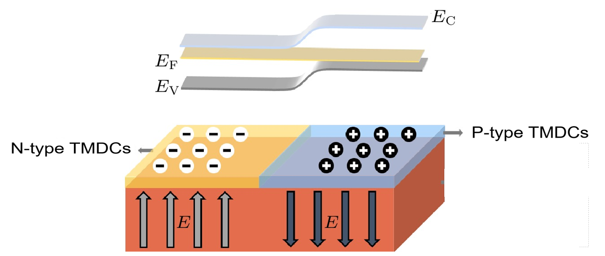
Figure 1. Schematic and band diagram of TMDCs homojunction based on electric field regulation [4].
3. Construction strategies
It is particularly important to prepare high-quality p-n homojunction to study the properties of p-n homojunctions and manufacture related devices.
Doping is a commonly used method in the chemical industry, usually referring to the purposeful addition of small amounts of other elements or compounds into a material or matrix to improve its performance. Doping can improve specific electrical, magnetic, and optical properties in materials and substrates, thereby giving them specific value or applications. In addition, because of the unique characteristics of 2D materials (quantum confinement effect), the number of atomic layers may be changed (change the thickness) to change the bandgap, which can further alter their properties. Due to the above reasons, there are four common methods for manufacturing p-n homojunction: chemical doping, elemental doping, electrostatic doping and thickness modulation. A brief introduction to these methods is as follows.
1) Chemical doping: The modification of a region's doping in a 2D material occurs when molecules, nanoparticles, or quantum dots adhere to the material's surface.
2) Elemental doping: Two layers for an identical two-dimensional substance with different levels of doping are stacked on top of one another to form an out-of-plane junction.
3) Electrostatically doped junctions: Local electrostatic gates are responsible for regulating the doping in various areas for an identical two-dimensional substance.
4) Thickness-based junctions: Two sections of the same material with differing thicknesses combine to generate the p and n regions [3].
3.1. Chemical doping
Due to the fact that molecules adsorbed on the surface of 2D materials can affect their transport through adding the effects of doping, consequently, by locally doping the 2D materials, a p-n junction may be created. Surface modulation, substitution, and intercalation are frequently used chemical doping techniques. Li et al used the inorganic molecule AuCl3 and the inorganic benzene viologen (BV) molecule to obtain a vertical p–n MoS2 homojunction [5]. It is a kind of p–n junction with charge transports out of plane. In this p-n junction, AuCl3 was p-doped on one face of a multilayer MoS2 flake, while BV was n-doped on the other. The MoS2 p-n homogeneous junction has various benefits over the unipolar MoS2 films, such as p-MoS2, n-MoS2, and pristine-MoS2. For example, it had an obvious rectifying consequence for charge carrier transportation. According to the final result properties, the current rectification ratio is approximately 100, and the theoretical fits point to an ideality factor (n) of 1.6.
3.2. Elemental doping
Elemental doping is a method that has succeeded in regulating carrier types in bulk materials. 2D materials can also be used with this technique. In addition, through extensive research, it has been found that 2D materials can also be used with this technique. For instance, a substitutional p-type or n-type dopant such as Nb (five valance electrons) or Re (seven valance electrons) has been employed to substitute the cation such as Mo or W with six valance electrons. This method is also feasible for 2D materials [6]. Additionally, by layering undoped MoSe2 on top of doped MoSe2 that has Nb atoms, Jin et al. built a p-n homojunction. Because of the low recombination rate at the clean homojunction interface, the p-n diode had an ideality factor of about 1.0 and a high external quantum efficiency of 52%, both of which improved in response to light intensity [7].
3.3. Electrostatic doping
Typically, local ionic gates, solid-state split grids, or ferroelectric polarization are used to modulate the carrier density and kind within various parts for an identical substance to accomplish electrostatic doping. For example, according to the configuration in this report, the voltage differential among the drain, source, and gate electrodes affects the doping type of the channel. The carrier is uniformly collected throughout the whole channel and forms an electron doping in the event that the gate voltage (Vgs) exceeds the drain voltage (Vds). Besides, adjacent patches on the channel surface that are doped with electrons and holes can be formed when the source, drain, and gate are each negatively and positively biased as well as the gate connects to the ground. Finally, the ionic motion will be fixed by reducing the ionic liquid's glass transition temperature, leading to the creation of a stable p-n homojunction [8]. According to the discussion above, monolayer or few-layer MoS2, WSe2, MoSe2, MoTe2, and black phosphorus (BP) are often employed for electrostatic doping to create homojunctions. This is likely because of their distinctive features including lower carrier level as well as ambipolar electric properties, which increase their susceptibility to external electrostatic field modulation also makes p-n homojunctions easier to create. In conclusion, using two-dimensional substances that have decreased carrier concentration along with changeable ambipolarity, electrostatically gated p-n homojunctions could get produced [6].
3.4. Thickness modulation
Unlike conventional materials, Due to quantum-confinement processes, the amount of bandgap energy in ultra-thin substances (such as 2D materials) becomes a thickness-dependent variable. Changing the thickness of the material can change the bandgap energy. As a result, when the p and n regions are constructed from identical substances but have distinct thicknesses, a p-n junction may be created. For instance, Sun et al. introduced a method of optimization that due to the exfoliation process, MoS2 flakes that already had various thickness regions (The thicknesses of the monolayer and multilayer MoS2 were 0.65 nm and 6.9 nm) were produced [9]. After observation and measurement, the junctions existed between flakes of different thicknesses. Therefore, this process can be used to produce the p-n junction based on thickness modulation.
4. Applications
New multifunctional electrical and optoelectronic devices are being developed with a lot of attention due to the two-dimensional homogenous junctions' exceptional features and distinctive structure. Numerous 2D homojunctions have beneficial characteristics, such as rapid transmission of charge plus the outstanding ability to sense light, offering a replacement for modern Si-based devices [2]. Next, several typical devices made of two-dimensional homogeneous junctions will be introduced.
4.1. Rectifiers
The rectifying feature of a p-n junction, which just permits carriers to travel in a single way, serves a crucial purpose. Based on this characteristic, p-n homojunction can be used to make rectifiers. Nowadays, many rectifiers have been made with p-n homojunctions and function quite well. For example, at a gate voltage of 0 V, a kind of vertical MoSe2 homojunction had a rectification ratio that was exceeding 106. That depended on the forward/reverse current ratio [10].
4.2. LEDs
In semiconductors, photonic emission may be produced as a result of the radiative recombination of electron-hole pairs to release their energy. To generate LEDs for lights, displays, and other uses, the energy may be employed. Ross et al. created the electroluminescent instrument employing a single-layer WSe2 p-n homojunction using separated gates formed by the dielectric h-BN [11]. When the device operated at Vg1 = Vg2 = 8 V with an excitation current of 5 nA, a brilliant electroluminescence emission zone surrounded the junction between the p-type and n-type areas.
4.3. Photodetectors
Currently, photodetectors with fast response, high sensitivity, and small size are needed. 2D homojunction, due to its excellent controllability, high plasticity, and outstanding physical properties, has become a good material for making photodetectors. An external electric field can be utilized by the photoconductive effect to encourage carrier split and transport, improving responsiveness and reaction rate as a result. Photodetectors designed using the effect have better performance. Huo et al. described a high-performance photodetector that makes utilization of a vertical MoS2 p-n homojunction [12]. For this type of detector, under visible illumination of 635 nm at Vds of 10 V and Vgs of 35 V, the channel conductance was affected by the positive photogate produced by the accumulating holes within the p-region. This special structure allows the device to produce an excellent photoconductive gain of over 105. In addition, its response performance is also very outstanding. It has a high responsivity of 7×10⁴ A W-1 with a fast response rate of 10 ms. The excellent photoconductivity and high response rate demonstrate excellent performance.
5. Challenges
Currently, for the manufacture of 2D p-n junctions, there are still numerous obstacles to be solved. The process that generates two-dimensional p-n junction on a large scale and the environmental deterioration of two-dimensional substances are the two biggest obstacles.
Firstly, one challenge is that many methods have been proven successful in experiments but are not suitable for commercial applications (such as chemical vapor deposition). Combining the development of single 2D materials with multiple doping strategies is a potential method for large-scaling the manufacture of two-dimensional p-n junctions [13].
Additionally, the environmental deterioration of many of the well-known 2D materials is a typical problem. For instance, black phosphorous in its ultrathin form has a tendency to absorb wet when exposed to air, which will degrade the material's electrical characteristics. Researching new packaging methods or using new 2D materials may solve the problem.
6. Conclusion
This article summarizes the structure of 2D p-n homojunction. Specifically, this article introduces the characteristics, classification, and preparation methods of 2D p-n homojunctions. In terms of construction strategies, chemical doping, elemental doping, electrostatic doping and thickness adjustment are all feasible to improve the properties. Then, it focuses on the use of applications in electrical and optical devices including rectifiers, LEDs and photodetectors. In addition, the challenges currently faced are also discussed.
However, there are still some challenges in large-scale commercial production of devices made of 2D p-n homojunctions. By improving production methods, encapsulation techniques, and researching novel materials, these difficulties may be overcome and large-scale commercial production can be achieved.
References
[1]. Li, C., Cao, Q., Wang, F., et al. 2018 Chemical Society Reviews, 47 4981-5037.
[2]. Wang, F., Pei, K., Li, Y., et al. 2021 Advanced Materials, 33 2005303.
[3]. Frisenda, R., Molina-Mendoza, A. J., Mueller, T., et al 2018 Chem Soc Rev, 47 3339-3358.
[4]. Shu Y, Zhang Y, Wang S. 2021 Acta Phys. Sin., 70 177301.
[5]. Li, H. M., Lee, D., Qu, D., et al. 2015 Nature Communications, 6 6564.
[6]. Suh, J., Park, T. E., Lin, D. Y., et al. 2014 Nano Letters, 14 6976-6982.
[7]. Jin, Y., Keum, D. H., An, S. J., et al. 2015 Advanced Materials, 27 5534-5540.
[8]. Zhang, Y. J., Oka, T., Suzuki, R., et al. 2014 Science, 344 725-728.
[9]. Sun, M., Xie, D., Sun, Y., et al. 2017 Scientific Reports, 7 4505.
[10]. Jin, Y., Keum, D. H., An, S. J., et al. 2015 Advanced Materials, 27 5534-5540.
[11]. Ross, J. S., Klement, P., Jones, A. M., et al. 2014 Nature Nanotechnology, 9 268-272.
[12]. Huo, N., & Konstantatos, G. 2017 Nature Communications, 8 572.
[13]. Kang, K., Xie, S., Huang, L., et al. 2015 Nature, 520 656-660.
Cite this article
Gu,Y. (2023). Advances in Two-Dimensional Materials for p-n Homojunctions. Applied and Computational Engineering,24,199-203.
Data availability
The datasets used and/or analyzed during the current study will be available from the authors upon reasonable request.
Disclaimer/Publisher's Note
The statements, opinions and data contained in all publications are solely those of the individual author(s) and contributor(s) and not of EWA Publishing and/or the editor(s). EWA Publishing and/or the editor(s) disclaim responsibility for any injury to people or property resulting from any ideas, methods, instructions or products referred to in the content.
About volume
Volume title: Proceedings of the 2023 International Conference on Functional Materials and Civil Engineering
© 2024 by the author(s). Licensee EWA Publishing, Oxford, UK. This article is an open access article distributed under the terms and
conditions of the Creative Commons Attribution (CC BY) license. Authors who
publish this series agree to the following terms:
1. Authors retain copyright and grant the series right of first publication with the work simultaneously licensed under a Creative Commons
Attribution License that allows others to share the work with an acknowledgment of the work's authorship and initial publication in this
series.
2. Authors are able to enter into separate, additional contractual arrangements for the non-exclusive distribution of the series's published
version of the work (e.g., post it to an institutional repository or publish it in a book), with an acknowledgment of its initial
publication in this series.
3. Authors are permitted and encouraged to post their work online (e.g., in institutional repositories or on their website) prior to and
during the submission process, as it can lead to productive exchanges, as well as earlier and greater citation of published work (See
Open access policy for details).
References
[1]. Li, C., Cao, Q., Wang, F., et al. 2018 Chemical Society Reviews, 47 4981-5037.
[2]. Wang, F., Pei, K., Li, Y., et al. 2021 Advanced Materials, 33 2005303.
[3]. Frisenda, R., Molina-Mendoza, A. J., Mueller, T., et al 2018 Chem Soc Rev, 47 3339-3358.
[4]. Shu Y, Zhang Y, Wang S. 2021 Acta Phys. Sin., 70 177301.
[5]. Li, H. M., Lee, D., Qu, D., et al. 2015 Nature Communications, 6 6564.
[6]. Suh, J., Park, T. E., Lin, D. Y., et al. 2014 Nano Letters, 14 6976-6982.
[7]. Jin, Y., Keum, D. H., An, S. J., et al. 2015 Advanced Materials, 27 5534-5540.
[8]. Zhang, Y. J., Oka, T., Suzuki, R., et al. 2014 Science, 344 725-728.
[9]. Sun, M., Xie, D., Sun, Y., et al. 2017 Scientific Reports, 7 4505.
[10]. Jin, Y., Keum, D. H., An, S. J., et al. 2015 Advanced Materials, 27 5534-5540.
[11]. Ross, J. S., Klement, P., Jones, A. M., et al. 2014 Nature Nanotechnology, 9 268-272.
[12]. Huo, N., & Konstantatos, G. 2017 Nature Communications, 8 572.
[13]. Kang, K., Xie, S., Huang, L., et al. 2015 Nature, 520 656-660.