


1. Introduction
When the channel is short enough, quantum tunneling can easily occur, causing electrons to move freely between the source and drain, even without a voltage boost, depriving the transistor of its switching function and rendering the logic circuit useless. FinFET was created to break the limitations of the 22nm process. FinFET is a novel complementary metal oxide semiconductor transistor. The technology was developed by Professor Zhengming Hu of the University of California, Berkeley. The main difference between FinFET and flat MOSFET architectures is that the channels consist of tall, thin fins raised on an insulating substrate. The source and drain poles are located at both ends of the channel, and there are three grids near the side wall and top of the channel for auxiliary current control. This finlike structure increases the surface around the entrance of the gate and strengthens the gate’s control over the entrance. Therefore, it can effectively alleviate the short channel effect in planar devices, greatly improve circuit control, reduce leakage current, and greatly shorten the transistor gate length. Due to this characteristic, FinFET does not require highly doped channels, so it can effectively reduce the scattering effect of impurity ions and improve the mobility of channel carriers. Ion implantation technology has been widely used in planar MOSFET, but it still faces some challenges in three- dimensional FinFET.
Owing to the fin on FinFET device, ion implantation needs to consider conformal doping, tilt angle, and the amorphization of fin by implantation, etc [1]. Based on these, this paper highlights two mainstream ion implantation methods in FinFET technology, and presents how the two technologies break through these challenges. After ion implantation, some amorphous silicon is still produced on the fins, which increases the resistance of the source drain zone and is not what we expected. So this requires the annealing step to solve this problem. After rapid annealing, defects will be well repaired and source and drain will be formed.
2. Short channel effect
As we said in the introduction, we want the chip have a good computational power, the only way to do this was increase the number of transistors in the chip. However the area of the chip was limited, so we have to reduce the area for the transistors, while for the planer transistor like MOSFETs, when the gate length is lower than 90nm, there will be a short channel effect occurs, and it was caused by 3 reasons that shows below [2].
2.1. Drain induced barrier lowering
We can see Figure 1 below that when the channel length decrease, the barrier (ϕB) of MOSFET will reduced, this means when channel length was too small the transistor will turn on early than we expect, and it was hard for engineer to design chips.
2.2. Saturation velocity
Saturation velocity was the maximum velocity for the carrier (holes or electrons) in semiconductor device [3], However in small scale device (<90nm), the high electrical field region will be smaller than average maen free path of the charge carrier, which will cause Velocity overshoot and hot carrier junction
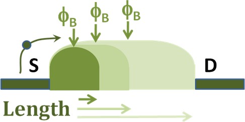
Figure 1. Drain induced barrier lowering.
2.2.1. Velocity overshoot. Briefly, Velocity overshoot was the transmit time for carrier between source and drain lower than the time for emission an optical phonon, the maximum transmit speed will be 3 times higher than saturation velocity [4]. Which causes transistor switch faster than normal, it will also make chip designer hard to design a chip.
2.2.2. Hot carrier junction. The Figure 2 below shows us what is Hot carrier junction, Hot carrier junction was the carrier in semiconductor get enough kinetic energy to go through the barrier, just like the graph shows to us the electron go through the oxide layer into the gate, and It will make a gate current, which will broken the MOSFET
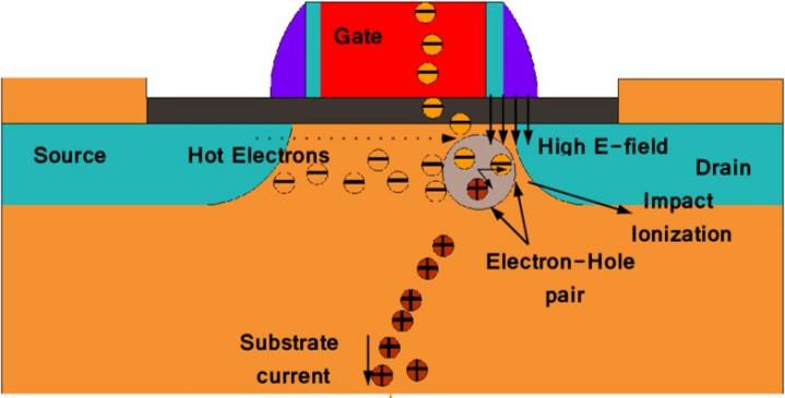
Figure 2. Hot carrier junction.
2.3. Quantum confinement
In Quantum mechanics, Quantum confinement can be observed when the diameter of the material was same as the de Brogile wavelength [5]. Mostly, when the diameter of the material was larger than de Brogile wavelength, the behavor of partical was freedom, and in this condition the bandgap of material will stay the same, However in small scale device, electron and hole will be squeezed into a dimension that approach to exciton Bohr radius and it will make the bandgap of the material large than normal.
3. Planer transistor and 3D transistor
The work function for Planer transistor and 3D transistor was same, However 3D transistor can figure out short channel effect, we can see Figure 3 that the gate for FinFET has three side and the effective length of it changes to
\( {W_{eff}} = H+W \)
where \( {W_{eff}} \) means the effective length of FinFET gate, \( H \) means the Fin Height and \( W \) means the Fin Width. It’s obvious that the effective length is longer than MOSFET in a limited area so we can use a limited area to create more transistors and those transistor can figure out short channel effect.
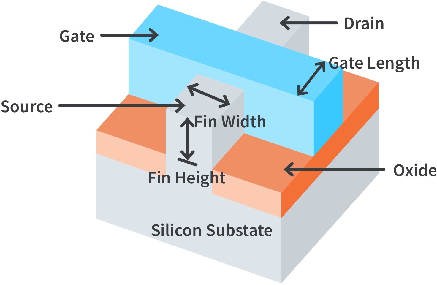
Figure 3. planer transistor to FinFET.
4. Source and drain formation in FinFETs– challenges and approaches
4.1. Ion Implantation in FinFETs
Nowadays the fabrication of planar MOSFETs has became really mature. In the whole fabrication process, the special doping technology—ion implantation—plays an crucial role in S/D formation in the planar FinFETs. However, there are numerous challenges on the transmission from the planar transistors to the 3D-structure FinFETs. The conformal doping and damage control will be the most important challenges [6].
4.1.1. Conformal doping. For FinFET structure, except for less dopant diffusion and profile abruptness, the conformal distribution within fins is a key part because the nonconformal doping profile results in degradation of the drive current of the transistor. The density of the fins and the thickness of each make the tilt angle more difficult to set, which results in the difficulty of achieving conformal doping.
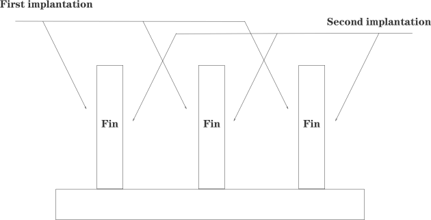
Figure 4. BLII in FinFET.
As shown in Figure 4, if the beam line ion implantation (BLII) method is used to implant the FinFET, since the FinFET is a nonplanar structure, the implantation needs to maintain a tilted angle. If the FinFET density is higher, it will result in a larger implantation angle, which during the process, there will be obvious sputtering phenomenon, which is easy to damage the Fin junction. The structure will be etched and the implant dose will be reduced at the same time.
Furthermore, if we were doping FinFETs with the same BLII technique, we would need to distribute the implants from both sides. This results in variations in the dopant dose on the sides and top of the fin, making it impossible to achieve conformal doping. If the angle needs to be continuously adjusted to achieve conformal doping, it will make the implantation process more complicated and difficult.
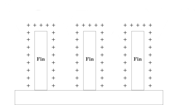
Figure 5. positive ions around the fin.
4.1.2. Plasma Immersion–an approach to improve conformality. When the whole device is immersed into plasma, the angle problem can be solved very well because the plasma state around the FinFET is uniform, a layer of positive ions will form around the surface of the fins (as shown in Figure 6), and these layers of positive ions will inward form an electric field vertical to the surface of the FinFET. In this way, the doping density of the side and top of the fin is uniform, that is, conformal doping is achieved. Besides, the plasma immersion ion implantation device becomes simpler.
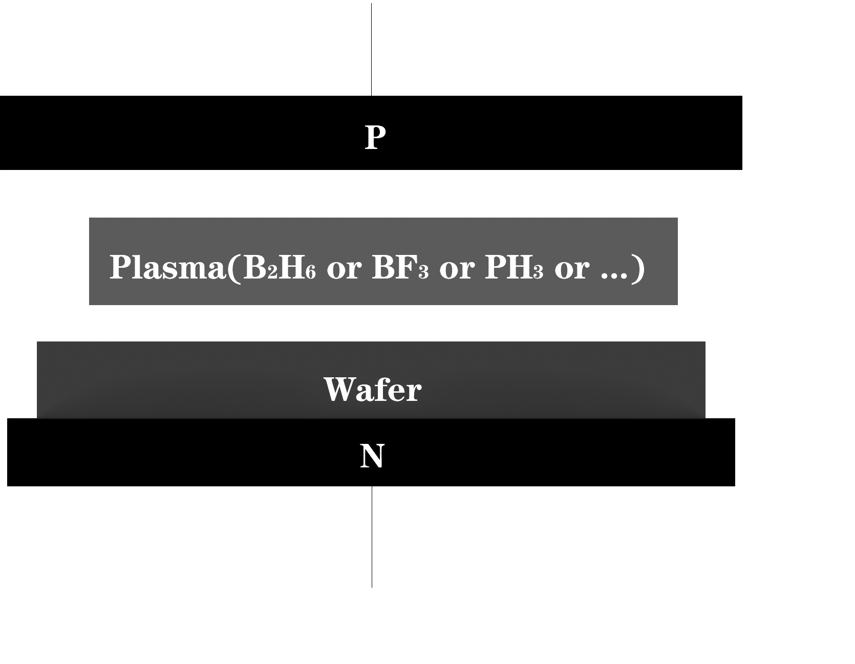
Figure 6. Schematic diagram of PIII.
To be more specific, its basic working principle is shown in Figure 5. The silicon wafer is placed in a vacuum chamber, an anode plate is set on the other side parallel to the silicon wafer, and the wafer is located at the cathode position. After the gas of heteroelements (such as BF2+), the gas molecules are ionized under the action of the electric field between the plates to form a plasma, and then a negative pulse voltage is applied to the wafer, so that the positive charges in the plasma pass through the sheath and enter the plasma among the wafers.
The Silicon Systems Group of Varian Semiconductor Equipment in USA has designed an experiment to the comparison between BLII and PIII.
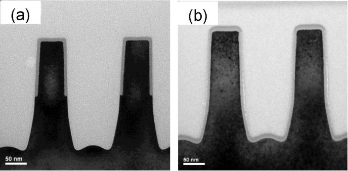
Figure 7. XTEM of 45° tilt beam line implant (a), novel doping (b) [7].
Figure 7 (a) and (b) indicate that BLII only amorphorizes partial of the fin while PIII successes in making silicon amorphization at the top and across the sidewall down to the bottom of the fin uniform and conformal.
4.1.3. Damage control. During the process of high dose tilt implantations in FinFETs, part of the Si fins will be amorphized. Different from planar transistor, the 3D structure of FinFETs make amorphous silicon recrystallization problematic. The amorphous fin will increase the source drain resistance of the device and degrade its electrical characteristics. Therefore, controlling over the fin damage by ion implantation becomes a must and a challenge.
4.1.4. Heated Ion Implantation–an approach to control the damage. To get better control over this issue, heated ion implantation is an alternative approach is doping the dopants on a heated silicon substrate. Its physical mechanism is, as mentioned above, that the increased substrate temperature suppresses the damage accumulation in the substrate, and thus attenuates the probability of amorphous layer formation.
| Figure 8. Schematic illustration of RT and heated Ion Implantation for Source and Drain formation in FinFETs [8]. |
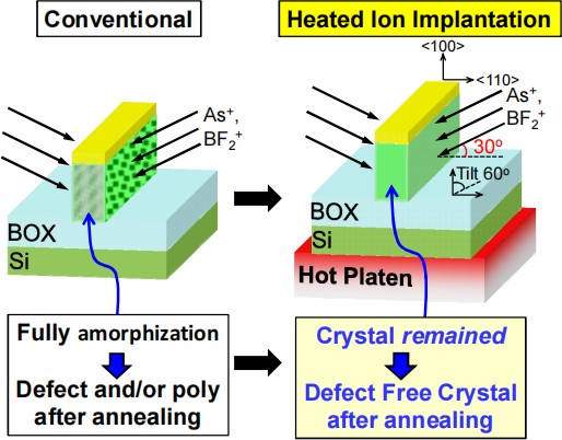
Figure 8 gives the comparison diagram of conventional injection at room temperature and high temperature and tells the single crystal condition of the implanted layer is maintained during heated ion implantation, and thus defect free crystal can be obtained by activation annealing. With the hot platen below the Silicon substrate, the FinFETs can be only amorphized partly, which can be eliminated after annealing.
| Figure 9. Comparison of the effects of heated ion implantation in FinFET devices. |
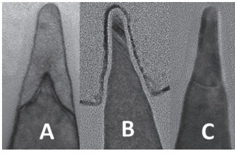
Figure 9 shows the effect comparison of the NMOS-FET heat implantation shown by Intel. A and B are the morphologies of the fin before and after annealing at room temperature implantation, respectively, and C is the TEM image after heat implantation It can be seen that the defect on the Fin after the heat implantation is significantly better than the normal temperature implantation.
| Figure 10. Amorphous Si thickness as a function of implantation temperature [9]. |
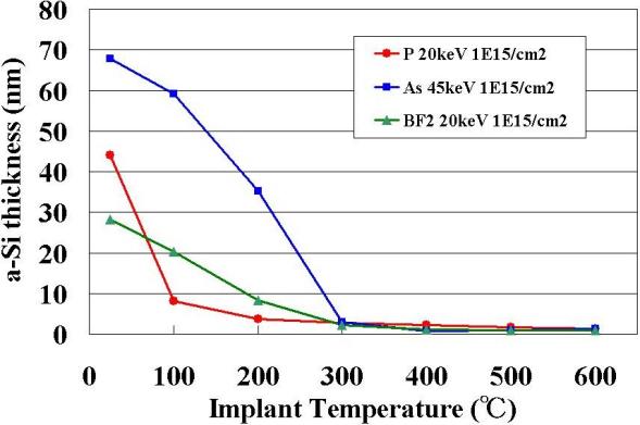
Temperature is an important condition parameter of hot implantation process. If the temperature is too high, energy will be wasted. If the temperature is too low, the doping effect will be poor. According to the experiments of NeRI in AIST on three doped substances–As, P+, and BF2+, it can be seen from Figure 10 that 300°C and over is the “key” temperature for keeping Si crystallineity. For different types of substrates and different dopants, it is very important to find the ”key” temperature.
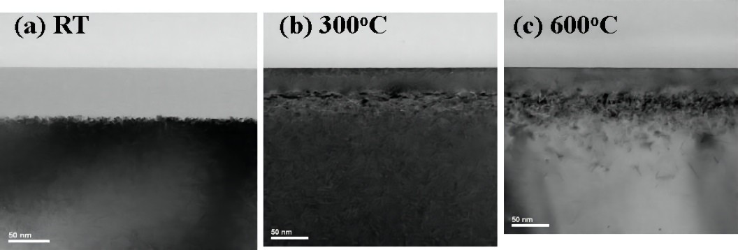
Figure 11. Cross sectional TEM results of As+ implanted at (a)RT, (b)300°C and (c)600°C [9].
The result of As+ implantation showed that the higher the temperature, the better the crystalline silicon was maintained. Two different approaches have been investigated. Because they solve two important problems in separate directions, the two approaches may be used together to achieve better ion implantation in the future. However, although ion-implantation methods can be improved, amorphous silicon still cannot be completely solved, and the subsequent annealing step then becomes critical.
4.2. Annealing in FinFETs
After ion implantation, high energy incident ions will collide with atoms on the semiconductor lattice, causing displacement of some lattice atoms and resulting in defects. The atoms in the implanted region will be disordered or become amorphous [10]. Therefore, the semiconductor must be annealed at a certain temperature and time after ion implantation to restore the crystal structure [11], eliminate defects and activate the implanted impurities.
With the development of integrated circuits, conventional thermal annealing methods can no longer meet the requirements because it cannot completely eliminate defects and will produce secondary defects. Long time in low temperature annealing will result in the growth of the defect size and widen the band width formed by the defect. In contrast, high annealing temperature will make defects growth seem to be terminated, but cannot be dissolved [12]. The annealing temperature must reach at least 1000 centigrade to fully activate some impurities, so modern integrated circuits prefer to Rapid Thermal Annealing (RTA)— a certain area of the silicon wafer is heated to the required temperature(>1000°C) in an instant and the annealing is completed in a short time (10−3 10−2s).
At present, the better RTA methods include pulse laser rapid annealing, pulse electron beam rapid annealing, ion beam rapid annealing, continuous wave laser rapid annealing and non-phase broadband light source (such as halogen lamp and electric gate heating) rapid annealing. The steps of RTA include: First, turn on the circulating water and pay attention to finding the correct circulating water. Second, pull out the sample holder and put the pieces, but do not tighten it for the time being. Thirdly, open the nitrogen knob and the nitrogen cylinder valve, tighten the sample holder and turn on the power supply, the fan and the key to on. Then, adjust power limit and upper limit and adjust the knob to set the multi-step annealing temperature and time. After that, press run and start to start annealing. After completion, “end” will be displayed, and then press run to repeat and adjust each knob to zero. After cooling, turn the key to off. Take the piece, tighten it, close the float flowmeter and close the bottle valve. Finally, turn off the power and circulating water.
After annealing, the implantation junction depth of planar silicon was measured by secondary ion mass spectrometry (SIMS) and the lattice damage and repair of the fin structure were tested by TEM [13].
After measuring, Figure 12(a) is local appearance of the fin sample before annealing. It is clear to find that there was a gray shadow around the fin, which was silicon dioxide. After implantation, lattice damage caused by implantation, occurring on both sides, were basically the same. The thickness of damage on the FinFET was 3 ∼ 5 nm.
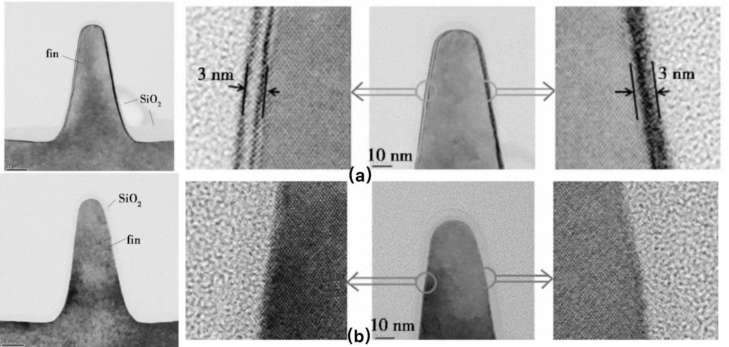
Figure 12. Local appearance of the fin sample before annealing(a) and after annealing(b) [13].
Figure 12(b) shows the local appearance of fin after annealing. The results showed that the lattice damage has been well-repaired after rapid annealing of the implanted samples. RTA technology can help the FinFET reduce hardness, residual stress, deformation and crack tendency after ion implantation, uniforming material structure and composition, improving material properties and preparing for future heat treatment. Therefore, rapid annealing can repair the damage of fin samples after ion implantation.
5. Conclusion
We mainly discuss the challenges in forming the source and drain regions and technical innovation of FinFET. Based on the structure of FinFET, this paper explains that FinFET can break through the short channel effect which planar transistor can not break through. Then, focusing on ion implantation and annealing process, the major challenges of transitioning from planar transistors to three-dimensional transistors and the solutions are described. It includes plasma immersion ion implantation method to solve the problem of common doping, thermal implantation to solve the problem of fin damage, and RTA annealing method to better remove fin amorphous.
Based on the innovation of FinFET 3D structure, many new structural forms of devices are being studied at present. The birth of FinFET is of great significance for the realization of transistors with narrower channels and higher performance in the future.
Acknowledgments
The authors are grateful to Prof. Yahong Xie for his guidance on theoretical knowledge and contribution to the main idea in this paper.
References
[1]. Radamson, H.H.; Zhang, Y.; He, X.; Cui, H.; Li, J.; Xiang, J.; Liu, J.; Gu, S.; Wang, G. The Challenges of Advanced CMOS Process from 2D to 3D. Appl. Sci. 2017, 7, 1047. https://doi.org/10.3390/app7101047
[2]. D’Agostino, Fabio, and Daniele Quercia. “Short-channel effects in MOSFETs.” Introduction to VLSI design (EECS 467) 70 (2000): 71- 72.
[3]. Peter, Y. U., and Manuel Cardona. Fundamentals of semiconductors: physics and materials properties. Springer Science & Business Media, 2010.
[4]. Jyegal, Jang. “Velocity overshoot decay mechanisms in compound semiconductor field-effect transistors with a submicron characteristic length.” AIP Advances 5.6 (2015): 067118.
[5]. Cahay, M. ” Quantum confinement VI: nanostructured materials and devices: proceedings of the international symposium.” The Electro- chemical Society, 2001.
[6]. M.I. Current, Ion implantation of advanced silicon devices: Past, present and future, Mater. Sci. Semicond. Process. 62 (2017) 13–22, https://doi.org/10.1016/j. mssp.2016.10.045
[7]. (jinmo)K. Han et al., ”A novel plasma-based technique for conformal 3D FinFET doping,” 2012 12th International Workshop on Junction Technology, 2012, pp. 35-37, doi: 10.1109/IWJT.2012.6212805.
[8]. W. Mizubayashi et al., ”Heated ion implantation technology for highly reliable metal-gate/high-k CMOS SOI FinFETs,” 2013 IEEE International Electron Devices Meeting, 2013, pp. 20.5.1-20.5.4, doi: 10.1109/IEDM.2013.6724670.
[9]. H. Onoda, W. Mizubayashi, Y. Nakashima and M. Masahara,”Heated ion implantation technology for FinFET application,” 2014 Interna- tional Workshop on Junction Technology (IWJT), 2014, pp. 1-6, doi: 10.1109/IWJT.2014.6842045.
[10]. Qumin, sun Shuai, Liu shuaixiu, pan Qiwei, Zhang Jing, Key appli- cations of ion implantation technology in nano integrated circuit tech- nology, Northern University of Technology, DOI:10.19353/j.cnki.dzsj, 2020.21.080
[11]. H. Onoda et al., Proc. 13th Int. Workshop on Junction Tech., 2013, pp. 66-69.
[12]. Hiroshi Onoda, * Wataru Mizubayashi, Yoshiki Nakashima and * Meishoku Masahara. Heated Ion Implantation Technology for FinFET Application, Nissin Ion Equipment Co., Ltd.
[13]. Zou Zhichao,Li Chaobo,Luo Jun,Xia Yang. Application of the Plasma Immersion Ion Implantation in FinFET Doping [A] . China; Chinese Academy of Sciences,2014
Cite this article
Li,B.;Xu,K.;Yu,X.;Li,Z. (2023). A review on source and drain formation in FinFETs. Applied and Computational Engineering,7,712-720.
Data availability
The datasets used and/or analyzed during the current study will be available from the authors upon reasonable request.
Disclaimer/Publisher's Note
The statements, opinions and data contained in all publications are solely those of the individual author(s) and contributor(s) and not of EWA Publishing and/or the editor(s). EWA Publishing and/or the editor(s) disclaim responsibility for any injury to people or property resulting from any ideas, methods, instructions or products referred to in the content.
About volume
Volume title: Proceedings of the 3rd International Conference on Materials Chemistry and Environmental Engineering (CONF-MCEE 2023), Part II
© 2024 by the author(s). Licensee EWA Publishing, Oxford, UK. This article is an open access article distributed under the terms and
conditions of the Creative Commons Attribution (CC BY) license. Authors who
publish this series agree to the following terms:
1. Authors retain copyright and grant the series right of first publication with the work simultaneously licensed under a Creative Commons
Attribution License that allows others to share the work with an acknowledgment of the work's authorship and initial publication in this
series.
2. Authors are able to enter into separate, additional contractual arrangements for the non-exclusive distribution of the series's published
version of the work (e.g., post it to an institutional repository or publish it in a book), with an acknowledgment of its initial
publication in this series.
3. Authors are permitted and encouraged to post their work online (e.g., in institutional repositories or on their website) prior to and
during the submission process, as it can lead to productive exchanges, as well as earlier and greater citation of published work (See
Open access policy for details).
References
[1]. Radamson, H.H.; Zhang, Y.; He, X.; Cui, H.; Li, J.; Xiang, J.; Liu, J.; Gu, S.; Wang, G. The Challenges of Advanced CMOS Process from 2D to 3D. Appl. Sci. 2017, 7, 1047. https://doi.org/10.3390/app7101047
[2]. D’Agostino, Fabio, and Daniele Quercia. “Short-channel effects in MOSFETs.” Introduction to VLSI design (EECS 467) 70 (2000): 71- 72.
[3]. Peter, Y. U., and Manuel Cardona. Fundamentals of semiconductors: physics and materials properties. Springer Science & Business Media, 2010.
[4]. Jyegal, Jang. “Velocity overshoot decay mechanisms in compound semiconductor field-effect transistors with a submicron characteristic length.” AIP Advances 5.6 (2015): 067118.
[5]. Cahay, M. ” Quantum confinement VI: nanostructured materials and devices: proceedings of the international symposium.” The Electro- chemical Society, 2001.
[6]. M.I. Current, Ion implantation of advanced silicon devices: Past, present and future, Mater. Sci. Semicond. Process. 62 (2017) 13–22, https://doi.org/10.1016/j. mssp.2016.10.045
[7]. (jinmo)K. Han et al., ”A novel plasma-based technique for conformal 3D FinFET doping,” 2012 12th International Workshop on Junction Technology, 2012, pp. 35-37, doi: 10.1109/IWJT.2012.6212805.
[8]. W. Mizubayashi et al., ”Heated ion implantation technology for highly reliable metal-gate/high-k CMOS SOI FinFETs,” 2013 IEEE International Electron Devices Meeting, 2013, pp. 20.5.1-20.5.4, doi: 10.1109/IEDM.2013.6724670.
[9]. H. Onoda, W. Mizubayashi, Y. Nakashima and M. Masahara,”Heated ion implantation technology for FinFET application,” 2014 Interna- tional Workshop on Junction Technology (IWJT), 2014, pp. 1-6, doi: 10.1109/IWJT.2014.6842045.
[10]. Qumin, sun Shuai, Liu shuaixiu, pan Qiwei, Zhang Jing, Key appli- cations of ion implantation technology in nano integrated circuit tech- nology, Northern University of Technology, DOI:10.19353/j.cnki.dzsj, 2020.21.080
[11]. H. Onoda et al., Proc. 13th Int. Workshop on Junction Tech., 2013, pp. 66-69.
[12]. Hiroshi Onoda, * Wataru Mizubayashi, Yoshiki Nakashima and * Meishoku Masahara. Heated Ion Implantation Technology for FinFET Application, Nissin Ion Equipment Co., Ltd.
[13]. Zou Zhichao,Li Chaobo,Luo Jun,Xia Yang. Application of the Plasma Immersion Ion Implantation in FinFET Doping [A] . China; Chinese Academy of Sciences,2014