


1. Introduction
With the emergence and widespread use of high-computing, high-data-volume tasks such as artificial intelligence, the problem of "memory walls" has arisen in the pursuit of larger, more accurate models. The need for more computing power and lower power consumption in industry has led to research into new computing and storage devices. The memristor, a new type of programmable, variable-resistance, two-terminal device, has attracted a great deal of attention and research is growing[1]. A variety of materials with such effects and applications are mentioned in several articles [2][3][4][5]. In the second chapter of this paper, the authors will summarize the mathematical principles and background of the memristor, as well as the application scenarios of the memristive system; for the Chapter 3, the author will introduce the 2 main mechanisms of changing resistance. In Chapter 4, the author will focus on the circuit design by memristor and its application in the field of artificial intelligence. Finally, in Chapter 5, the authors will look at the prospects of memristors. This paper focuses on summarizing the properties and principles of memristor and its current research status in the field of artificial intelligence, providing a corresponding reference for researchers in this field.
2. Mathematical principles and background of memristor
An ideal memristor is a passive 2 terminal electronic device, which has the property of changeable resistance. In other words, the ideal memristor can remember the amount of current (magnetic flux) flow through it and perform it as the resistance it has. The ideal memristor is first predict by Professor Chua in 1971 as the fourth fundamental circuit element. The basic and important mathematical definition and the prediction of its features which will be discuss below [1]. However, the ideal memristor device only existed on mathematical model, and there was no direct correlation between the concept and the behavior of certain materials under certain conditions, resulting in no more systematic studies over the next 30 years. Until 2008, in HP's materials lab, researchers discovered that the i-v curve of a dropped titanium dioxide film sandwiched between two platinum electrodes looked like a Lissajous-Figure, as shown in Figure 1 [6]. They found that the memristor model proposed by Professor Chua in 1971 could well explain the special phenomenon of this material. Their discovery was the beginning of the practical use of memristors and led to the subsequent extensive research on memristors.
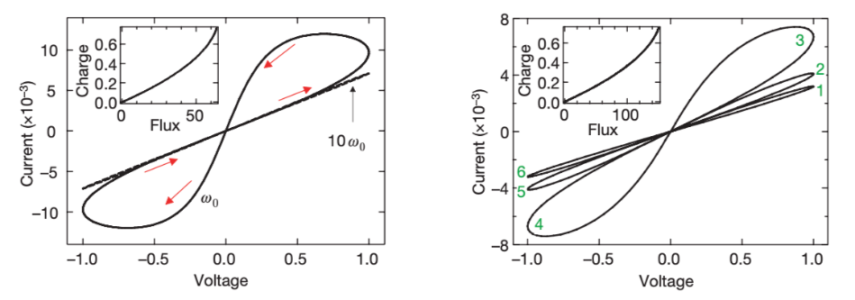
Figure 1. The i-v of new 2-terminal devices [7].
In 1971, Professor Chua postulated, based on symmetry, that there should be six different mathematical equations for the four fundamental quantities in a circuit, namely charge \( q \) , voltage \( v \) , current \( i \) and magnetic flux \( φ \) [8]. Specifically,
Resistance ( \( R \) ): \( dv=R∙di \)
Inductance ( \( L \) ): \( dφ=L∙di \) (1)
capacitance ( \( C \) ): \( dq=C∙dv \)
As well as 2 physics law: Faraday's law of electromagnetic induction: \( ε=\frac{dφ}{dt} \) , The differential equation for current: \( i=\frac{dq}{dt} \) .
However, the relationship between magnetic flux and electric charge has been slow to be confirmed. As Professor Chua mentioned in his seminal paper, he felt that it was essential to define the relationship between magnetic flux and charge, both mathematically and logically. And, as can be seen in Figure 2, it was necessary to fill in the gaps in the circles from the point of view of symmetry.
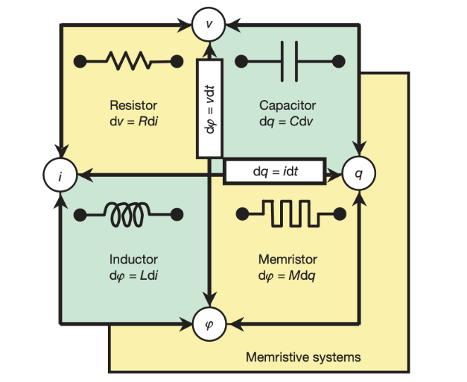
Figure 2. The 4 basic quantities and 5 different relationships [7].
This figure led to give yet another definition of the fourth basic circuit element.
\( g(φ, q)=0 \) (2)
Since the magnetic flux can be a single-valued function of the charge, the opposite is true: the charge can also be a single-valued function of the magnetic flux. From this, Professor Chua derived the expressions corresponding to the current(charge)-controlled memristor and the voltage(flux)-controlled memristor by the derivation shown below. This opens this promising and exciting field.
2.1. Current-controlled memristor
If the definition \( g(φ, q)=0 \) is treated as a single-valued function of charge \( q \) , then, this kind of memristors is known as the ideal current-controlled memristors, or, in some literature, referred to as a charged-controlled memristor. There is not much difference between the two terms.
Here, memristance is defined as the resistance of a current-controlled memristor. This is the mathematical equation:
\( M(q)=\frac{dφ(q)}{dq} \) (3)
If moving \( dq \) to the left-hand side of the equation and take the derivative of both sides with respect to time \( t \) :
\( M(q)∙\frac{dq}{dt}=\frac{dφ(t)}{dt} \) (4)
Then, memristance and expressions related to voltage and current can be obtained:
\( v(t)=M(q(t))∙i(t) \) (5)
From the results obtained, memristance and resistance have the same dimension. This is why it is considered that memristor is a basic component of variable resistance. Theoretically speaking, at a certain point in time, memristance is only a function about q(t). Therefore, memristance can be regarded as a value determined by the properties of the material itself at this time node, and the current or voltage at this time are variables [9]. However, with the change of time, q(t), as a function of the amount of charge passing through memristor, is likely to change, and thus, the resistance value of memristor will change accordingly. From the derivation results, the ideal current-controlled memristor is a passive device that responds to the amount of charge passed before and can achieve the purpose of memorizing data.
2.2. Voltage-controlled memristor
Voltage-controlled memristor is a kind of ideal memristor model, as same as above, it also has the property of changeable resistance(conductance) values. In some other literature, the voltage-controlled memristor is also called the flux-controlled memristor. The flux here refers to the magnetic flux.
The conductance of an ideal voltage-controlled memristor refers to memductance:
\( W(φ)=\frac{dq(φ)}{dφ} \) (6)
Doing the same operation above, the ideal voltage-controlled memristor can be expressed as following:
\( i(t)=W(q(t))∙v(t) \) (7)
Memductance has the same dimension as conductance in a circuit. In addition, memductance is a single-valued function of u(t), in other words, magnetic flux changes with time, and corresponding voltage (Faraday electromagnetic induction) will be generated. While the ideal voltage-controlled memristor will remember the voltage through it, reflected as a memductance change [10]. Like the ideal current-controlled memristor, the memristor's unique controllable, programmable changes make the circuit design more exciting.
2.3. Memristive system
In the above section, the authors have reviewed two theoretical memristor models, which are mathematically equivalent in terms of their derivation. It is very difficult to implement the ideal memristor. However, since there are many materials with memristor-like characteristics, the important concept of a memristive system was introduced in 1976. This article generalized the boundaries of the memristor and made the theory applicable to a wider range of materials and devices [1]. For example, in a broad sense, Redox-based memristive devices (ReRAM), Conductive-bridge random access memory (CBRAM), The Thermistor, metal-insulator transition devices (MIT), phase-change memory (PCM), magnetoresistive RAM (MRAM) and ferroelectric RAM (FeRAM) can all be considered as a memristive system.
The memristive system has a wide range of applications and before discussing the applications, the author will briefly summarize the memristive system as defined by Professor Chua. As a more generalized memristor system, the memristive system extends the basic properties of the memristor with a state variable, often called w, which describes the physical properties of the system at any given moment. This leads to the first equation of the memristive system, called the dynamical equation, which states that the state variable is a time varying function and has the expression:
\( \frac{dw}{dt}=f(w,i,t) \) (8)
This leads to the second equation (9), the quasi-static conduction equation, which shows the nature of the resistance variation of the ideal memristor that the memristive system has, and which relates the resistance of the memristive system's This expression extends the influence of the resistance of a memristive system by the expression:
\( v(t)=R(w, i, t)∙i(t) \) (9)
These two equations (8) and (9) are the fundamental principles that determine the nature of a memristive system. By determining the state variable of a memristive system, the nature of the whole system is determined.
In general, the state variable is determined by the properties of the material itself, as in the case of the titanium dioxide thin film memristor, where the state variable is defined as:
\( \frac{dw(t)}{dt}={μ_{V}}\frac{{R_{ON}}}{D}i(t) \) (10)
Where the \( {R_{ON}} \) is the resistance of high dopants area, and \( {μ_{V}} \) is the average ion mobility in a uniform filed [2].
According to the authors' findings and conclusions, the applications of memristive systems can be divided into three main areas, namely high performance computing, including in-memory computing, neurotrophic computing, etc.; information storage, including various applications such as RAM (mentioned above), which are part of memristive systems; and finally, non-linear circuits, mainly in chaotic circuits, providing reliable true random numbers for secure communication networks, information encryption, etc. RAM; and finally, the field of non-linear circuits, mainly in chaotic circuits, providing reliable true random numbers for applications such as secure communication networks and information encryption.
The first category is non-volatile memory, which has the characteristics of large capacity and low speed and is usually used as a storage medium for long term information as information can be saved after power is removed. DRAM, Static Random Access Memory (SRAM), etc., are usually used as temporary storage media for computer processing information due to their high-speed characteristics. However, in scenarios where there is a high demand for data transfer (e.g., artificial intelligence training, high performance cloud computing, etc.), there are often situations known as "memory walls" that limit the maximum performance of the computer. This has led to the need for high-speed, non-volatile memory. As early as 2014, research has shown that memristive systems can be used as a new type of storage device with basic information storage capabilities. Various memristive systems, such as ReRAM, CBRAM, etc., have carried the expectations of researchers. The industry has also shown great interest in these new memories that combine the fast characteristics of volatile memory with the long-term data retention properties of non-volatile memory.
Due to the inherent non-linear nature of the memristive system, it is an excellent choice for references to non-linear circuits such as chaotic circuits. The idea of using memristors to build chaotic circuits was proposed as early as 2009. A year later, a researcher implemented a chaotic circuit based on memristors by means of an analogue circuit[11]. In the same year, a researcher proposed a chaotic circuit using two energy storage elements, namely an inductor and a capacitor, and a memristor[12]. However, in 2010, a researcher introduced time-lag feedback into the recently created memristor circuit and succeeded in creating a circuit with a chaotic form[13]. Thanks to the uncontrollable randomness of chaotic circuits, the resulting true random numbers are promising for applications in chaotic communication, network encryption, financial security, and other areas where cryptography is highly desirable.
3. Mechanisms and model of memristor
The mechanisms by which the resistance of the memristor varies are very rich, and many of them still need to be investigated in more depth and detail and are very promising. At present, the prevailing classification of memristors is based on three categories of mechanisms, namely the dot effect, the ionic effect, and the thermal effect. When a voltage is applied to the ends of a memristor, an electric field is created in the device material, and a certain amount of Joule heat is generated, all of which influence the resistance change of the memristor. In general, devices containing the first two effects are more widespread and are now the primary mechanism for amnesic resistors [citation needed], but most cases are the result of a combination of several conditions. In this chapter, the authors will focus mainly on the value change memory (VCM), and introduce two widely used models, the Filament Model, and the interface model, which are widely reported.
The valence change memory or mechanism (VCM) involves two different efforts, one is associated with localized material conduction properties and the other with changes across the material interface. The local variation is the filament model, which is described below, while the interface is the interface model.
3.1. Conductive filament model
This model was first proposed very early, even before the concept of the memristor was introduced[8]. In the filament model, there are also metallic and vacancies. The metal type is the more common and familiar type of resistive phenomenon. Most teams produce a structure which usually consists of two electrodes and a dielectric layer sandwiched between them, thus forming a complete amnestic resistor with variable resistance properties. In order to achieve the conductivity of the filament, attention is paid to the selection of the electrodes, which are an active electrode and an inert electrode on the other side, prepared from an active metal and an inert pure metal respectively.
The formation of the conductive filament channel is achieved by first applying a high voltage to the electrode, which breaks through the intermediate dielectric layer[9], a process known as forming. As the channel is formed, it is then possible to control the on/off of the channel using a positive or negative voltage, a process known as Set and Reset, as illustrated in Figure 3.
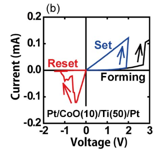
Figure 3. Set and Reset [11].
Specifically, this is a redox reaction in which the metal atoms in the active electrode are separated from the electrode by the presence of an external electric field and form ions, which then travel with the resulting channel to the inert electrode on the other side and are eventually reduced to the original metal atoms, a process which varies according to the magnitude of the electric field and is similar when the voltage is applied in reverse. This process varies according to the magnitude of the electric field and is similar when the voltage is applied in the opposite direction, thus achieving a change in the resistance of the material.
As these effects usually occur at the microscopic level. Thus, it is important to use special techniques for observation. It has been documented that teams have used scanning thermal microscopy (SThM) to directly observe the formation of filament [5], while others have used a scanning transmission electron microscope (STEM) and a transmission electron microscope (TEM) to obtain clear images of filament [14], the team also used the energy-dispersive X-ray spectroscopy (EDX) to test the formation of filaments on the material. The team also used the energy-dispersive X-ray spectroscopy (EDX) to test whether the material formed filaments.
3.2. Interface model
In the interface model, it is mainly the ionic utility that plays an important role. Firstly, the amnesia based on the interface model has a similar structure to the opportunity filament model mentioned above, in that a dielectric film is sandwiched between two electrodes. However, the difference is that in the interface model, the material of the dielectric film is often not identical throughout the structure [15]. Usually, a part of the material is hybridized during fabrication to include more ions, thus altering the new conductivity of the material, and forming an intrinsic semiconductor similar to that formed by electrons (in this case too many anions) or holes (in the case of amnesic resistors, the incorporated cations). By applying a voltage at both ends of the material, the ions are brought closer to the corresponding electrodes in the presence of an external electric field. For example, for a device with an anion (nowadays mainly oxygen ions are added as anions), the ions will gradually move to the positive end of the electrode, and if the electric field is homogeneous, the movement of the ions can be represented macroscopically as a thin film moving. This results in a change in the thickness of the part of the dielectric layer of the device that is mixed and the part that is not, with the part that is mixed with the anion generally being more conductive and the part that is not being mixed showing weak conductivity. As a result, the whole structure of the memristor changes with the electric field, resulting in a change in the resistance of the memristor. When the power supply is removed, the distribution of ions in the memristor does not change due to the withdrawal of the electric field, as the ions are additionally intercalated, unlike in p-n junctions where a stable layer is formed between the materials, thus achieving the purpose of memory.
This interface model has been described by detailed mathematical equations, as in the case of the titanium dioxide thin-film device made by HP's laboratory in 2008, which was mentioned earlier. The state variable is defined in relation to the migration rate of electrons and has the expression:
\( \frac{dw(t)}{dt}={μ_{V}}\frac{{R_{ON}}}{D}i(t) \) (11)
At the same time, they have incorporated oxygen ions in a part of the titanium dioxide film, as illustrated in Figure 4.
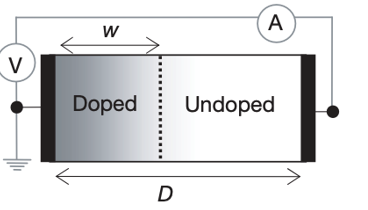
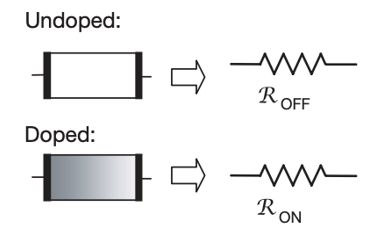
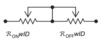
Figure 4. The memristor with interface model [7].
The resistance value of the doped part of the film is set to \( {R_{ON}} \) and that of the undoped part is set to \( {R_{OFF}} \) , which gives the expression:
\( v(t)=({R_{ON}}\frac{w(t)}{D}+{R_{OFF}}(1-\frac{w(t)}{D}))i(t) \) (12)
4. Application
As research into the biological brain progressed over the last century, the idea of artificial neurons was proposed. Subsequent developments have gradually moved away from the complete simulation of the way the biological brain works. However, with the widespread study of memristors, the properties of memristors have made it more realistic to implement neural networks through hardware. In this chapter, the authors will first briefly review models of the biological brain and current neural networks, then describe 2 ways of implementing 2 basic logic gates via RRAM, and finally summarize some of the results of recent research teams on memristor-based neural networks.
4.1. Brain and neural network
In the figure 5 below, sketch a model of a biological neuron.
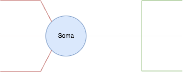
Figure 5. The model of a neuron in the brain.
The blue circles represent the soma of the neuron, which is the main part of processing information and is mainly processed in a non-linear manner. Around soma, highlighted in red, are neuronal dendrites that collect signals from other neurons, usually bioelectrical signals. After a series of operations, if the value exceeds a threshold, the neuron sends a signal through its axon (shown in green) to other neurons. This builds the neural networks in the biological brain.
Similarly, by and large, neural network models are now made up of many neurons. Similarly, to the biological brain, each artificial neuron has a non-linear activation function.
\( y=f(\sum {w_{i}}{x_{i}}) \) (13)
where y is the output value, xi is the input from the \( {i^{th}} \) element of the previous layer and \( {w_{i}} \) is the weight of \( {x_{i}} \) . f can be several different functions, and in practice, non-linear activation functions such as ReLU and Softmax, shown in Figure 6.
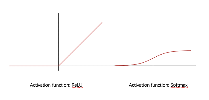
Figure 6. Graph of activation function: ReLU and Softmax.
This is similar to how neurons in the brain are treated in a non-linear way. Different algorithms, such as the widely used gradient descent algorithm, are used to change the values in the weight matrix for the purpose of training the neural network. In the training process, unlike the biological brain, artificial neural networks require many matrix multiplications and a large amount of data input, giving rise to a tricky problem called the memory wall. This has led to concepts such as in-memory computing, which are still in the exploratory stage.
4.2. Three logic gates design based on RRAM
The logic gate in Figure 7(c) is the AND gate. it uses an external voltage as an input and is calculated by means of an external circuit that detects the node voltage. Therefore, this logic gate is called a \( V-V \) logic gate [4]. For a given input voltage \( {V_{input}} \) on a single component, the current through it can be expressed as:
\( {I_{m}}=\frac{1}{{R_{m}}}{V_{m}} \) (14)
Where \( {V_{m}} \) is \( {V_{input}}-{V_{share}} \) , assuming that there is a voltage \( {V_{share}} \) at the common terminal of the different components. The expression for the individual component current can be written as:
\( {I_{m}}={G_{m}}({V_{input}}-{V_{share}}) \) (15)
Also, considering the ground of the component group, for \( {V_{share}} \) then there would be:
\( {V_{share}}-0V={R_{L}}{I_{L}} \) (16)
Where \( {I_{L}}=\sum {I_{m}} \) , bringing in the previous expressions one finds that:
\( {V_{share}}={R_{L}}\sum {G_{m}}({V_{input}}-{V_{share}}) \) (17)
Finally, combining \( {V_{share}} \) :
\( {V_{share}}=\frac{1}{{G_{L}}+\sum {G_{j}}}\sum {G_{j}}{V_{j}} \) (18)
The output voltage requires additional circuitry for processing before it can be used. The final output voltage is a function of \( {V_{share}} \) and the dashed line in Figure 7indicates the range of the final output's output voltage.
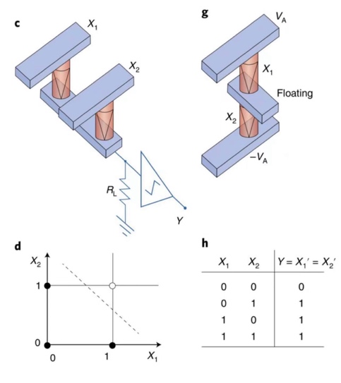
Figure 7. Logic gates based on RRAM [9].
In Figure 7 is a combination of two RRAMs, where the arrow points to a state where the resistance value of the RRAM changes to LRS when a negative voltage is applied. In this combination, the input value X is presented in the resistive state of the RRAM (HRS is 1 and LRS is 0. It can be noticed that there is and only is no voltage drop when both RRAMs connected in series are in the on state. It is only in the intermediate floating part that the threshold is not exceeded. The component is thus an OR gate implemented by RRAMs.
5. Conclusion
In this paper, the authors introduce the principles of memristor and memristive system, present two common principal models and describe the application of memristor in the field of neural networks. In summary, memristor is a new type of semiconductor material that has developed rapidly over the last 15 years, with many materials with memristor properties being discovered and many memristor-given array integrated circuits being fabricated. memristor has basically formed a chain of research and pilot production. Although there are still several process, material and cost drawbacks, the authors are optimistic that memristor will be able to be commercialized on a large scale. The authors have a positive attitude towards the large-scale commercialization of memristors. With the application of various advanced artificial intelligence technologies, the market for low and medium power platforms will grow like never before. The high concurrency and low power consumption of memristor will make its development in low and medium power platforms more promising. The author agrees that memristor will become one of the computing platforms for artificial intelligence.
References
[1]. L. Chua, “Memristor-The missing circuit element,” IEEE Transactions on Circuit Theory, vol. 18, no. 5, pp. 507–519, 1971.
[2]. B. Muthuswamy and P. Kokate, “Memristor-Based Chaotic Circuits,” IETE Technical Review, vol. 26, no. 6, p. 417, 2009.
[3]. E. Zhang, “New conduction and reversible memory phenomena in thin insulating films,” Pro-ceedings of the Royal Society of London. Series A. Mathematical and Physical Sciences, vol. 301, no. 1464, pp. 77–102, Oct. 1967.
[4]. H. Akinaga and H. Shima, “Resistive Random Access Memory (ReRAM) Based on Metal Ox-ides,” Proceedings of the IEEE, vol. 98, no. 12, pp. 2237–2251, Dec. 2010.
[5]. J. H. Park, H.-D. Kim, S. M. Hong, M. J. Yun, D. S. Jeon, and T. G. Kim, “Improved resistive switching phenomena observed in SiNx-based resistive switching memory through oxygen doping process,” physica status solidi (RRL) - Rapid Research Letters, vol. 8, no. 3, pp. 239–242, Dec. 2013.
[6]. Q. Shen et al., “Linear and nonlinear interface rheological behaviors and structural properties of pea protein (vicilin, legumin, albumin),” Food Hydrocolloids, vol. 139, p. 108500, May 2023.
[7]. Strukov, Dmitri B., et al. “The Missing Memristor Found.” Nature, vol. 453, no. 7191, May 2008, pp. 80–83.
[8]. L. O. Chua and Sung Mo Kang, “Memristive devices and systems,” Proceedings of the IEEE, vol. 64, no. 2, pp. 209–223, 1976.
[9]. J. Sun, J. Li, Y. Wang, X. Zhang, and G. Cui, “Area of Pinched Hysteresis Loops for Current-Controlled Memristor and Voltage-Controlled Memristor,” Journal of Computational and Theoretical Nanoscience, vol. 12, no. 11, pp. 4335–4339, Nov. 2015.
[10]. N. V. Morozovsky, “Voltage controlled awakening of memristor-like dynamic current–voltage loops of ferroelectric triglycine sulfate,” Applied Physics Letters, vol. 118, no. 19, p. 192902, May 2021.
[11]. F. Corinto and A. Ascoli, “Memristor based-elements for chaotic circuits,” Nonlinear Theory and Its Applications, IEICE, vol. 3, no. 3, pp. 336–356, 2012.
[12]. T. Matsumoto, L. O. Chua, and S. Tanaka, “Simplest chaotic nonautonomous circuit,” Physi-cal Review A, vol. 30, no. 2, pp. 1155–1157, Aug. 1984.
[13]. B. Karakaya, A. Gülten, and M. Frasca, “A true random bit generator based on a memristive chaotic circuit: Analysis, design and FPGA implementation,” Chaos, Solitons & Fractals, vol. 119, pp. 143–149, Feb. 2019.
[14]. H. Tian et al., “Extremely Low Operating Current Resistive Memory Based on Exfoliated 2D Perovskite Single Crystals for Neuromorphic Computing,” ACS Nano, vol. 11, no. 12, pp. 12247–12256, Dec. 2017.
[15]. I. Valov, R. Waser, J. R. Jameson, and M. N. Kozicki, “Electrochemical metallization memo-ries—fundamentals, applications, prospects,” Nanotechnology, vol. 22, no. 28, p. 289502, Jun. 2011.
Cite this article
Li,H. (2023). The memristor: Principle, mechanism, and application. Applied and Computational Engineering,28,110-118.
Data availability
The datasets used and/or analyzed during the current study will be available from the authors upon reasonable request.
Disclaimer/Publisher's Note
The statements, opinions and data contained in all publications are solely those of the individual author(s) and contributor(s) and not of EWA Publishing and/or the editor(s). EWA Publishing and/or the editor(s) disclaim responsibility for any injury to people or property resulting from any ideas, methods, instructions or products referred to in the content.
About volume
Volume title: Proceedings of the 2023 International Conference on Mechatronics and Smart Systems
© 2024 by the author(s). Licensee EWA Publishing, Oxford, UK. This article is an open access article distributed under the terms and
conditions of the Creative Commons Attribution (CC BY) license. Authors who
publish this series agree to the following terms:
1. Authors retain copyright and grant the series right of first publication with the work simultaneously licensed under a Creative Commons
Attribution License that allows others to share the work with an acknowledgment of the work's authorship and initial publication in this
series.
2. Authors are able to enter into separate, additional contractual arrangements for the non-exclusive distribution of the series's published
version of the work (e.g., post it to an institutional repository or publish it in a book), with an acknowledgment of its initial
publication in this series.
3. Authors are permitted and encouraged to post their work online (e.g., in institutional repositories or on their website) prior to and
during the submission process, as it can lead to productive exchanges, as well as earlier and greater citation of published work (See
Open access policy for details).
References
[1]. L. Chua, “Memristor-The missing circuit element,” IEEE Transactions on Circuit Theory, vol. 18, no. 5, pp. 507–519, 1971.
[2]. B. Muthuswamy and P. Kokate, “Memristor-Based Chaotic Circuits,” IETE Technical Review, vol. 26, no. 6, p. 417, 2009.
[3]. E. Zhang, “New conduction and reversible memory phenomena in thin insulating films,” Pro-ceedings of the Royal Society of London. Series A. Mathematical and Physical Sciences, vol. 301, no. 1464, pp. 77–102, Oct. 1967.
[4]. H. Akinaga and H. Shima, “Resistive Random Access Memory (ReRAM) Based on Metal Ox-ides,” Proceedings of the IEEE, vol. 98, no. 12, pp. 2237–2251, Dec. 2010.
[5]. J. H. Park, H.-D. Kim, S. M. Hong, M. J. Yun, D. S. Jeon, and T. G. Kim, “Improved resistive switching phenomena observed in SiNx-based resistive switching memory through oxygen doping process,” physica status solidi (RRL) - Rapid Research Letters, vol. 8, no. 3, pp. 239–242, Dec. 2013.
[6]. Q. Shen et al., “Linear and nonlinear interface rheological behaviors and structural properties of pea protein (vicilin, legumin, albumin),” Food Hydrocolloids, vol. 139, p. 108500, May 2023.
[7]. Strukov, Dmitri B., et al. “The Missing Memristor Found.” Nature, vol. 453, no. 7191, May 2008, pp. 80–83.
[8]. L. O. Chua and Sung Mo Kang, “Memristive devices and systems,” Proceedings of the IEEE, vol. 64, no. 2, pp. 209–223, 1976.
[9]. J. Sun, J. Li, Y. Wang, X. Zhang, and G. Cui, “Area of Pinched Hysteresis Loops for Current-Controlled Memristor and Voltage-Controlled Memristor,” Journal of Computational and Theoretical Nanoscience, vol. 12, no. 11, pp. 4335–4339, Nov. 2015.
[10]. N. V. Morozovsky, “Voltage controlled awakening of memristor-like dynamic current–voltage loops of ferroelectric triglycine sulfate,” Applied Physics Letters, vol. 118, no. 19, p. 192902, May 2021.
[11]. F. Corinto and A. Ascoli, “Memristor based-elements for chaotic circuits,” Nonlinear Theory and Its Applications, IEICE, vol. 3, no. 3, pp. 336–356, 2012.
[12]. T. Matsumoto, L. O. Chua, and S. Tanaka, “Simplest chaotic nonautonomous circuit,” Physi-cal Review A, vol. 30, no. 2, pp. 1155–1157, Aug. 1984.
[13]. B. Karakaya, A. Gülten, and M. Frasca, “A true random bit generator based on a memristive chaotic circuit: Analysis, design and FPGA implementation,” Chaos, Solitons & Fractals, vol. 119, pp. 143–149, Feb. 2019.
[14]. H. Tian et al., “Extremely Low Operating Current Resistive Memory Based on Exfoliated 2D Perovskite Single Crystals for Neuromorphic Computing,” ACS Nano, vol. 11, no. 12, pp. 12247–12256, Dec. 2017.
[15]. I. Valov, R. Waser, J. R. Jameson, and M. N. Kozicki, “Electrochemical metallization memo-ries—fundamentals, applications, prospects,” Nanotechnology, vol. 22, no. 28, p. 289502, Jun. 2011.