


1. Introduction
The development of integrated circuits (ICs) has revolutionized modern electronic technology, transforming the technology, economy, and life patterns of humans. Initially divided into analog and digital signal circuits, ICs evolved into digital-analog mixed-signal circuits to adapt to the interaction between the physical and digital worlds. The design process for mixed-signal digital-analog ICs is complex and requires combining digital and analog components for overall considerations and verification. This paper uses literature review and case study methods to explore the potential of mixed digital-analog circuits in communication systems, intelligent electronics, aerospace, and other applications. The paper aims to analyze the difficulties and breakthroughs in digital-analog mixed signal circuit design, revealing potential areas of development potential and highlighting the stagnant development of integrated circuits. The aim is to explore the potential of mixed digital-analog circuits in various fields, clarify the stagnant development of integrated circuits, provide a reference for future research, and promote the development of mixed digital-analog circuit design.
2. Overview of analog-digital mixed signal circuits
2.1. Basic concepts and characteristics
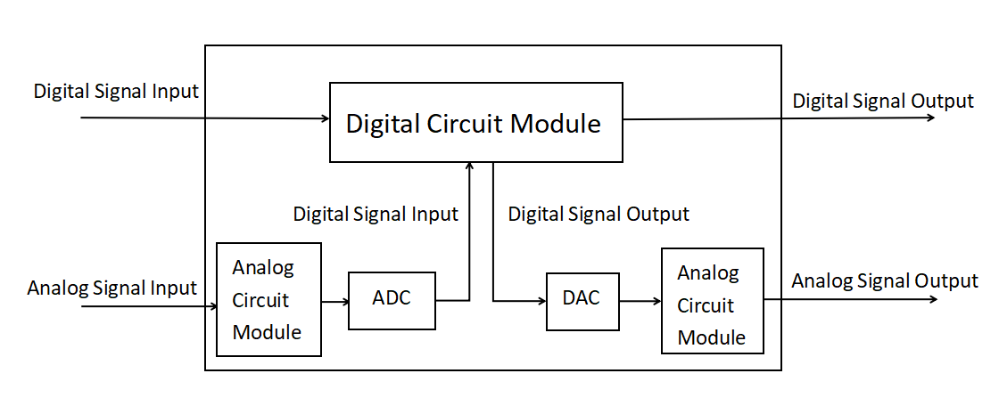
Analog signals are continuous changes in information transmitted through circuits like capacitors, resistors, and transistors. They are used for amplification, signal arithmetic, processing, and measurement. Digital signals, on the other hand, are discontinuous and represent binary numbers. Analog-digital mixed circuits combine analog and digital circuits, achieving continuous analog signals and discrete digital signals. Analog circuits offer high-precision signal recognition and wide-bandwidth processing, while digital circuits offer strong anti-jamming ability, programmability, and storage capabilities, enabling more complex functions in modern electronic systems follow figure 1.
2.2. Application areas and development trends
Based on the advantage that analog-digital mixed signal circuits can receive and process both analog and digital signals at the same time, analog-digital mixed signal circuits are more and more widely used and have achieved technological breakthroughs and project innovations in many fields.
2.2.1. Applications of analog-digital mixed signal circuits
Infrared communication technology has been widely used in a variety of short-distance communication, but most of the traditional infrared communication is in the form of digital coding, transmission of a single content, Hu Xuguang used the method of frequency division multiplexing to achieve the transmission of analog signals and digital signals in the same infrared physical channel to achieve the transmission of voice through the infrared channel in the transmission of digital at the same time [1]. Liao Chen et al. improved the reliability and stability of downhole coupling communication systems by demodulating the baseband signal through a front-end analog circuit and achieving accurate synchronization by detecting the M-sequence in the digital domain, thereby enhancing the reliability of these systems [2]. The application of analog hybrid digital circuits in communication systems makes up for the shortcomings of a single digital signal in traditional communication, enriches the types of transmitted signals, improves the stability of the communication system, and provides a feasible path for intelligent communication and voice control. Automotive electronic control systems require high reliability and high demand for chips. The TMS320C2812 core CPU is often used for automotive energy assembly control, but Burr-Brown's DAC7625 digital-to-analog converter is needed for analog outputs in hybrid cars [3]. High-power integrated circuits are widely used in automotive electronics, and rigorous compressive and automated testing is required to ensure reliability. Analog-digital mixed signal circuits, based on digital circuits, memory, analog circuits, and digital-to-analog/analog-to-digital conversion circuits, contribute to the completeness and low cost of automotive smart power integration testing [4]. Yu-Shi Chen developed an 8-bit, 500MS/s 2b/cycle analog-to-digital converter (ADC) for telemedicine communication systems. The ADC, based on successive approximation register architecture, meets conversion speed and accuracy requirements for evolving communication standards, providing reliable technical guarantee for high-speed data transmission in telemedicine services like tele-consultation and tele-surgery [5].
2.2.2. Trends in analog-digital mixed signal circuits
An analog-digital mixed signal circuit (HIC) is a circuit system where components with different functions are mounted on the same substrate. As electronic devices become more miniaturized and high-performance, there is a growing need to package functional components inside HICs. High density is a key feature of HICs, reflected in high-density circuit layout and interconnections. High-density packaging techniques like Flip-Chip or Chip Stacking increase package density but also increase heat dissipation difficulties. Designing and implementing thermal paths is critical for analog-digital mixed signal circuits with large output power. Overall, package design is moving towards high integration, high performance, and low power consumption [6].
3. Analog-digital mixed signal circuit design difficulty analysis
3.1. Noise interference from digital signal circuits to analog signal circuits
Mixed-signal integrated circuits have two main noise floors: Johnson-Nyquist noise (broadband noise) and flicker noise (low-frequency noise) [7]. Noise issues in analog sub-system design, particularly with digital-analog hybrid chips, are exacerbated by process miniaturization, feature size reduction, and low-voltage design. Digital circuits cause disturbances through charge leakage, capacitive crosstalk, and power integrity disturbances, with CMOS providing a low-resistance path for noise propagation [8].
Of these three types of disturbances, charge leakage and power disturbances propagate primarily through the substrate, while capacitive coupling is transmitted through the interconnect structure, together threatening the performance of sensitive analog circuits [9].
3.2. Effects of process deviations and device mismatches on circuit performance
IC manufacturing involves complex processes such as sub-wavelength lithography, random doping, etc. The instability of the process itself, environmental differences, and equipment errors are prone to process deviations. Such deviations exist not only between different devices within a single chip but also between different chips on the same wafer, different wafers, and different batches of products. Process deviations directly impact the electrical and physical properties of the transistors and the shape of the connecting wires, and these deviations become more noticeable as the size of the features gets smaller [10]. On-Chip Variation (OCV) is a significant factor affecting chip performance, particularly in analog signal integrated circuits. OCV is primarily manifested as device mismatches due to physical process deviations or random fluctuations in manufacturing. Factors affecting base breakdown voltage include collector doping concentration, collector thickness, device structure, size, process, and temperature. Parameter mismatches can cause signal delays or integrity problems in digital circuits, while in analog circuits, they can cause circuit failure. Examples include current-mirror circuits, differential amplifiers, and operational amplifiers [11].
3.3. Low power design challenges
Low-power design is crucial in the technology sector due to energy constraints and resource limitations. Portable devices like smartphones, smartwatches, and wireless headphones require low power consumption to extend their lifespan. The rise of IoT intelligent voice interaction technology has led to the deployment of micro-small IoT voice-aware nodes for voice recognition in homes and workplaces. These nodes, powered by smaller-capacity batteries, pose energy constraints and power consumption issues. In analog-digital mixed signal circuits, power consumption is divided into static and dynamic sources, with static power consumption due to DC power consumption of ADCs and DACs, and dynamic power consumption due to energy loss during charge charging and discharging [12].
4. Breakthrough directions in analog-digital mixed signal circuit design
4.1. Novel circuit architectures and design methodologies
4.1.1. Novel circuit architectures for analog circuits and novel storage for digital circuits
Mixed-signal integrated circuits face challenges due to analog circuit design issues, including incomplete EDA, poor automation, and manual labor. Traditional CMOS transistors struggle with leakage, power consumption, and stability. Fin FET devices offer a solution with zero-doped or low-doped channels for high integration in modern chips. Fin FET device (Fin Field-Effect Transistor, Fin Field-Effect Transistor) is a new type of 3D transistor, its channel using zero-doped or low-doped, the channel is surrounded by the gate on all three sides, this special three-dimensional three-dimensional structure, enhance the gate on the channel control, greatly inhibit the short-channel effect, and thus inhibit the leakage current of the device [13]. Fin FET-based design of analog-digital mixed signal circuits means that lower power consumption, higher speed and higher integration density can be achieved. Advanced analog device technology includes vertically stacked CFETs, symmetrical transmission, GaN-based HEMT devices, and two-dimensional FET sub-threshold swing breakthrough limit for ultra-low-power biosensing. TFET (Tunneling FET) to expand the dynamic range of low-voltage analog circuits [14]. Mixed-signal integrated circuits (ICs) are undergoing a paradigm shift in three dimensions: device structure to three-dimensional integration, design methodology to AI-assisted process evolution, and system architecture to autonomous reconfigurable multifunctional upgrades, enabling adaptive hardware in smart sensors and cognitive radio.
4.1.2. Automated circuit design based on neural networks and reinforcement learning
The continuous innovation in integrated circuit (IC) design methodologies is propelling electronic design automation (EDA) technology into an intelligent transformation phase. Confronted with design challenges posed by billion-scale transistors and multi-physical field coupling, traditional rule-based EDA tools struggle to address the exponential growth of solution-space search problems. In recent years, deep learning technology has provided a new paradigm for breaking through this dilemma, especially the integration of graph neural networks (GNN) and reinforcement learning (RL), which is reconfiguring the underlying logic of physical design [15]. The layout and wiring problem is essentially an ultra-large-scale combinatorial optimization problem, whose solution space dimension grows super-linearly with the design scale, far beyond the search capability of traditional heuristic algorithms. For instance, Junchi Yan proposes a DeepPlace layout framework based on reinforcement learning and GNN, i.e., the layout automation process of macromodules and standard cells is accomplished by the gradient optimization formed by reinforcement learning and neural networks, respectively [16]. Building on GNN, Google integrated the method into the reinforcement learning architecture to realize the encoding of different states, and successfully applied the method to the design flow of Google's self-developed Tensor Processing Unit (TPU), and obtained a degree of perfection as good as that of the circuit designed by experts [17].
4.2. Advanced process technology and packaging technology
Integrated chips using System on Chip (SOC) technology face challenges in performance improvement and multifunctionality, including reducing manufacturing costs and product yields. Companies like TSMC and Intel have proposed using different processes to manufacture different cores and integrate multiple cores in packaging. Advanced packaging technology aims at multiple chips or core particles for integration and packaging, with advanced 3D integration technology being the most advanced [18]. Silicon photonic integration technology uses semiconductor silicon and its derivatives as the optical medium substrate, combining high-density integration characteristics with high-frequency and wide-bandwidth advantages. This technology is a typical representative of digital-analog mixed-signal circuits [19]. Technological development is moving towards a breakthrough in monolithic photovoltaic integration, focusing on technical challenges such as heterogeneous material lattice matching, thermal stress regulation, and synergistic optimization of photovoltaic devices [20].
4.3. Low power design techniques
Low power consumption is crucial, and common designs include Power Gating, Dynamic Voltage Frequency Regulation (DVFS), and Clock Gating. Power gating controls power supply by switching power when idle, eliminating static consumption. It is suitable for intermittent operation, like cell phone Bluetooth. However, noise generation and wake-up delay need improvement. Dynamic Voltage and Frequency Scaling (DVFS) adjusts voltage and frequency based on circuit load, maximizing efficiency. This is ideal for dynamic workloads, like CPU and GPU workloads in computers. However, complex control circuits are needed to monitor workload and adjust voltage and frequency.
5. Conclusion
This paper discusses the application of analog-digital hybrid circuits in various fields, focusing on their advantages over single analog or digital circuits, their application in communication systems, automotive electronics, and other fields, and their development trend towards integrated, high-performance, and low-power circuit design. It also analyzes difficulties in analog-digital hybrid circuit design, such as noise interference, process deviations, device mismatches, and low-power design challenges. The paper also highlights breakthroughs in hybrid analog-digital circuits, such as the construction of a new three-dimensional FinFET circuit framework, evolving process and packaging technologies, neural network integration, digital memories, and low-power technologies. However, the review study on digital and analog hybrid circuits has shortcomings, including a lack of comparisons and introductions of innovative designs based on neural networks and circuit automation design. Future research should focus on enhancing the advantages of mixed analog-digital circuits and improving experimental data collection and organization.
References
[1]. Hu, X. G., Tao, K., & Deng, B. W. (2015). Design of analog-digital hybrid infrared channel communication device. Electronic Products World, 22(12), 27-29+36.
[2]. Liao, C. (2020). Anti-interference demodulation circuit for underground coupling communication. Electronic Production, (19), 12-17.
[3]. Tang, J. G., Wang, Y. N., Yang, H. Q., et al. (2007). Design and implementation of digital-analog conversion system for hybrid electric vehicles. Process Automation Instrumentation, (7), 17-20.
[4]. Wang, X. W. (2010). Research on low-cost testing technology for automotive intelligent power integrated circuits (Doctoral dissertation). Fudan University.
[5]. Chen, Y. S. (2022). Research on key technologies of mixed-signal integrated circuits for mobile healthcare (Doctoral dissertation). Xidian University.
[6]. Ji, M. N., Chang, M. C., Jia, Z. J., et al. (2024). Development trends and reliability evaluation methods for high-density hybrid circuit packaging technology. Integrated Circuits and Embedded Systems, 24(7), 25-29.
[7]. Lü, T., & Chen, R. (2010). Optimization analysis of crosstalk and substrate coupling noise in hybrid circuits. Electronic Process Technology, 31(3), 154-157.
[8]. Guo, R. (2015). PCB anti-interference design for digital-analog hybrid circuits. Mechanical and Electrical Information, (18), 146-147.
[9]. Zhang, Z. X. (2017). Research on methods to reduce interference in CMOS analog-digital circuits. Science and Technology Innovation Herald, 14(7), 27+29.
[10]. Yu, M. (2016). Design of bandgap reference voltage source based on process variation (Master’s thesis). Zhejiang University.
[11]. Zhang, J. H., Su, J. T., Xie, W. Y., et al. (2024). Analysis of load mismatch effects on heterojunction bipolar transistor devices based on waveform testing. High Power Laser and Particle Beams, 36(1), 34-40.
[12]. Zhang, H. (2011). Design and implementation of low-power and high-precision audio digital-to-analog converter (Master’s thesis). Zhejiang University.
[13]. Zhang, X. Q. (2017). Logic circuit design based on FinFET devices (Master’s thesis). Ningbo University, Zhejiang.
[14]. Deng, Z. H. (2024). Overview of integrated circuit technology. Integrated Circuits and Embedded Systems, 24(1), 1-12.
[15]. Tian, C. S., Chen, L., Wang, Y., et al. (2023). Research progress on electronic design automation technology based on graph neural networks. Journal of Electronics and Information Technology, 45(9), 3069-3082.
[16]. Shi, H. X., Zhu, J. C., Yan, J. C., et al. (2021). Customer repurchase prediction method based on convolutional neural network and LSTM recurrent neural network. High Technology Letters, 31(7), 713-722.
[17]. Mirhoseini, A., Goldie, A., Yazgan, M., et al. (2021). A graph placement methodology for fast chip design. Nature, 594(7862), 207-212.
[18]. Wang, G. W., Li, L., Pan, P. H., et al. (2025). Research and application status of multi-die 2.5D/3D integration technology. Journal of the University of Electronic Science and Technology of China. Advance online publication. https: //doi.org/ [insert DOI if available]
[19]. Guo, J., Feng, J. B., & Cao, G. W. (2017). Development and challenges of silicon photonics chip processes and design. ZTE Technology Journal, 23(5), 7-10.
[20]. Wu, B. B., Zhang, H. Y., Tang, X. H., et al. (2017). Research on silicon photonics technology and industry development. World Telecommunications, (2), 36-41.
Cite this article
Wan,K. (2025). Difficulties and Breakthroughs in the Design of Analog-digital Mixed Signal Circuits for Integrated Circuits. Theoretical and Natural Science,134,7-12.
Data availability
The datasets used and/or analyzed during the current study will be available from the authors upon reasonable request.
Disclaimer/Publisher's Note
The statements, opinions and data contained in all publications are solely those of the individual author(s) and contributor(s) and not of EWA Publishing and/or the editor(s). EWA Publishing and/or the editor(s) disclaim responsibility for any injury to people or property resulting from any ideas, methods, instructions or products referred to in the content.
About volume
Volume title: Proceedings of CONF-APMM 2025 Symposium: Controlling Robotic Manipulator Using PWM Signals with Microcontrollers
© 2024 by the author(s). Licensee EWA Publishing, Oxford, UK. This article is an open access article distributed under the terms and
conditions of the Creative Commons Attribution (CC BY) license. Authors who
publish this series agree to the following terms:
1. Authors retain copyright and grant the series right of first publication with the work simultaneously licensed under a Creative Commons
Attribution License that allows others to share the work with an acknowledgment of the work's authorship and initial publication in this
series.
2. Authors are able to enter into separate, additional contractual arrangements for the non-exclusive distribution of the series's published
version of the work (e.g., post it to an institutional repository or publish it in a book), with an acknowledgment of its initial
publication in this series.
3. Authors are permitted and encouraged to post their work online (e.g., in institutional repositories or on their website) prior to and
during the submission process, as it can lead to productive exchanges, as well as earlier and greater citation of published work (See
Open access policy for details).
References
[1]. Hu, X. G., Tao, K., & Deng, B. W. (2015). Design of analog-digital hybrid infrared channel communication device. Electronic Products World, 22(12), 27-29+36.
[2]. Liao, C. (2020). Anti-interference demodulation circuit for underground coupling communication. Electronic Production, (19), 12-17.
[3]. Tang, J. G., Wang, Y. N., Yang, H. Q., et al. (2007). Design and implementation of digital-analog conversion system for hybrid electric vehicles. Process Automation Instrumentation, (7), 17-20.
[4]. Wang, X. W. (2010). Research on low-cost testing technology for automotive intelligent power integrated circuits (Doctoral dissertation). Fudan University.
[5]. Chen, Y. S. (2022). Research on key technologies of mixed-signal integrated circuits for mobile healthcare (Doctoral dissertation). Xidian University.
[6]. Ji, M. N., Chang, M. C., Jia, Z. J., et al. (2024). Development trends and reliability evaluation methods for high-density hybrid circuit packaging technology. Integrated Circuits and Embedded Systems, 24(7), 25-29.
[7]. Lü, T., & Chen, R. (2010). Optimization analysis of crosstalk and substrate coupling noise in hybrid circuits. Electronic Process Technology, 31(3), 154-157.
[8]. Guo, R. (2015). PCB anti-interference design for digital-analog hybrid circuits. Mechanical and Electrical Information, (18), 146-147.
[9]. Zhang, Z. X. (2017). Research on methods to reduce interference in CMOS analog-digital circuits. Science and Technology Innovation Herald, 14(7), 27+29.
[10]. Yu, M. (2016). Design of bandgap reference voltage source based on process variation (Master’s thesis). Zhejiang University.
[11]. Zhang, J. H., Su, J. T., Xie, W. Y., et al. (2024). Analysis of load mismatch effects on heterojunction bipolar transistor devices based on waveform testing. High Power Laser and Particle Beams, 36(1), 34-40.
[12]. Zhang, H. (2011). Design and implementation of low-power and high-precision audio digital-to-analog converter (Master’s thesis). Zhejiang University.
[13]. Zhang, X. Q. (2017). Logic circuit design based on FinFET devices (Master’s thesis). Ningbo University, Zhejiang.
[14]. Deng, Z. H. (2024). Overview of integrated circuit technology. Integrated Circuits and Embedded Systems, 24(1), 1-12.
[15]. Tian, C. S., Chen, L., Wang, Y., et al. (2023). Research progress on electronic design automation technology based on graph neural networks. Journal of Electronics and Information Technology, 45(9), 3069-3082.
[16]. Shi, H. X., Zhu, J. C., Yan, J. C., et al. (2021). Customer repurchase prediction method based on convolutional neural network and LSTM recurrent neural network. High Technology Letters, 31(7), 713-722.
[17]. Mirhoseini, A., Goldie, A., Yazgan, M., et al. (2021). A graph placement methodology for fast chip design. Nature, 594(7862), 207-212.
[18]. Wang, G. W., Li, L., Pan, P. H., et al. (2025). Research and application status of multi-die 2.5D/3D integration technology. Journal of the University of Electronic Science and Technology of China. Advance online publication. https: //doi.org/ [insert DOI if available]
[19]. Guo, J., Feng, J. B., & Cao, G. W. (2017). Development and challenges of silicon photonics chip processes and design. ZTE Technology Journal, 23(5), 7-10.
[20]. Wu, B. B., Zhang, H. Y., Tang, X. H., et al. (2017). Research on silicon photonics technology and industry development. World Telecommunications, (2), 36-41.