


1. Introduction
The trend of daily electronic equipment puts forward important requirements for the development of original miniaturization. Low-dimensional nanomaterials have great potential in this application, which is expected to replace copper and metal as another option of integrated circuit interconnection materials. Since graphene can be prepared, it has attracted many scholars to conduct research on two-dimensional materials, and then the research of phosphorene has pushed the research and application of two-dimensional materials to an exciting height. And the quasi-one-dimensional nanoribbons materials then came into people’s vision. Quasi-one-dimensional nanoribbon structures caused by the edge configuration have unique electrical and magnetic properties different from two-dimensional materials. Among them, the study of graphene nanoribbons and phosphorene nanoribbons are two very important topics in the study of quasi-one-dimensional nanoribbon materials.
The properties of graphene are exceptional. The mobility and even ballistic transport of it at room temperature have been demonstrated, and it is patentable and scalable. Due to its lack of gaps, graphene cannot be utilised as such in digital electronics, which require high current on/off ratios [1]. And the graphene nanoribbons can effectively solve the related problems. Graphene nanoribbons are graphene bands with nanoscale width, which can be classified as zigzag graphene nanoribbons and armchair graphene nanoribbons based on their various edge configurations. The quantum domain limit effect caused by the nanoscale and the edge effect caused by the edge configuration can regulate the electronic properties of graphene nanoribbons and open the band gap of graphene. The opening in the nanoribbon can improve the current on/off ratios [1].
The puckered honeycomb layers of phosphorus atoms form the black phosphorus, which are bound together by van der Waals interactions and has similar structural characteristics to graphene. It is the most stable form of this element at room temperature. In contrast to graphene, phosphorene shows certain advantages in terms of fabricate edge-defect-free nanoribbons with controlled chirality. As a new type of low-dimensional material, black phosphorene nanoribbons have some strange physical properties, such as excellent electrical, optical and mechanical properties. It can adjust the electronic and transport properties of the nanoribbon structure by means of doping, applied stress or edge passivation.
Black phosphorene nanoribbons have some good advantages over graphene nanoribbons, for example, black phosphorene nanoribbons make up for the zero-band gap of graphene nanoribbons. However, with the in-depth study of two quasi-one-dimensional materials in recent years, graphene nanoribbon has no phosphorus loss strength in terms of electronic properties and transport properties. This research aims to review and summarize the latest research achievements of graphene nanoribbons and phosphorene nanoribbons in the electronic properties and transport properties. Compare the current performance advantages and possible applications of graphene nanoribbons with phosphorene nanoribbons.
2. Principle and influencing factors of graphene nanoribbon energy gap
Graphene is a carbon nanomaterial that shows two-dimensional honeycomb lattice structure [2]. If the size of graphene is limited in a certain direction, a ribbon structure is formed, called graphene nanoribbons, which is another one-dimensional nano-carbon structure besides carbon nanotube and carbon chain. The width of graphene nanoribbons is minimum to below 1nm; when the width is less than 10nm, it has unique properties. As shown in the Figure 1, According to the different edge arrangement mode and considering the high symmetry, graphene nanoribbons can be mainly divided into armchair type graphene nanoribbons and zigzag type graphene nanoribbons. Graphene itself has high mobility and high-current-carrying capabilities. Therefore, for the application of graphene nanoribbons in the field of electronic components, the most important thing is the preparation and improvement of the band gap.
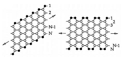
Figure 1. Representation of a zigzag (left) and armchair nanoribbon (right). The arrows indicate the long direction of the ribbons [1].
However, the band gap of armchair graphene and the band gap of zigzag graphene have completely different origin principles. Quantum confinement create a band gap in GNRs with armchair shaped edges, in which edge effects play an important role. For GNRs, when spin ordered states exist at the borders of GNRs, the band gaps result from a staggered sublattice potential [3].
Armchair graphene nanoribbons (AGNRs) have considerable band gaps up to 2.3 eV and are inversely proportional in size and width. The band gaps of GNRs with armchair-shaped edges are a result of quantum confinement [3]. The band gap of Na-AGNRs is closely related to its width (Na is the number of double bonds in the width direction of AGNRs, as a positive integer). As shown in the Figure 2a, according to the number of dimer lines (Na) on the band width, the armchair graphene nanoribbons can be divided into three categories: Na=3p, 3p+1, and 3p+2, where the p is a positive integer. According to the TB calculation, at Na=3p + 2, AGNR is metal type and the other two are semiconductor type. The band gap size is sorted as Na=3p>Na=3p+1>Na=3p+2. According to the calculation of first principles, the three types of AGNRs are semiconductor type, the order of the three band gap masters is unchanged, the difference is that Na=3p+2 band gap size is no longer zero. In two different calculation methods, the band gap of three classes of AGNRs decreases with increasing width.
For serrated graphene nanoribbons (ZGNRs), the band gap is also correlated with the width. The band gap size is zero when the width is less than the critical width, and a hundred meV when the width is greater than the critical width, and the critical width is generally a few nanometers [3]. ZGNRs generate the band gap of electrons on the hexagonal lattice because of the energy gap created by the staggered sublattice potential. It can also classify the zigzag graphene nanoribbons, ribbons with zigzag shaped edges on both sides are classified by the number of the zigzag chains (Nz) across the ribbon width, as shown in Figure 2b. The electron spins at the left and right edges of the ZGNRs are in opposite directions and its electron spin polarization leads to the appearance of ferromagnetic coupling and antiferromagnetic coupling. The overall energy difference between the couplings between ferromagnetic and antiferromagnetic edges reduces as Nz rises. Additionally, if the width is much greater than the spin-polarized edge states’ decay length, it eventually becomes insignificant [3].
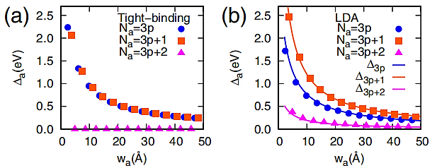
Figure 2. The variation of band gaps of Na-AGNRs as a function of width ( \( {w_{a}} \) ) obtained (a) from TB calculations with t=2.70(eV) and (b) from first-principles calculations (symbols) [3].
3. Factors influencing the energy gap in the black phosphorene nanoribbon
Black phosphorus is a direct bandgap semiconductor with a layered structure, which is combined by van der Waals forces. A less layer of black phosphorus is called phosphorene. Because of the interlayer weak van der Waals force interaction, phosphorene is easily obtained by mechanical stripping mass method. In the structure of a monolayer of phosphorene, each phosphorus atom is connected to the surrounding three phosphorous atoms by covalent bonds, forming a wrinkled honeycomb-like structure. Black phosphorene nanoribbons have some good advantages over graphene nanoribbons, because graphene has no intrinsic band gap, and even methods such as chemical modification of graphene often can only open a small band gap, and it is easy to reduce its carrier mobility. Phosphorene belongs to a semiconductor with intrinsic direct band gap. Its energy gap is about 1 eV, and the theoretical carrier mobility of phosphorene is as high as, which is currently the second only two-dimensional material to graphene. For this reason, a lot of research work on black phosphorene nanoribbons is focused.
Similar to graphene nanoribbons, phosphorene nanoribbons (PNR) can also be divided into zigzag phosphoene nanoribbons and armchair phosphoene nanoribbons. According to the common symbol labeling method, the width of the nanoribbons can be determined by the number of nanoriblayers Na. Studies have shown that the conductive properties of PNR depend on its edge properties. For phosphorene nanoribbons with no saturation at the edge, due to the hanging bond, the edge of the phosphorus atoms is reconstructed, the structure of Zig zag-type black phosphorus nanoribbons (ZPNR) shows metal characteristics, while Armchair-type black phosphorus nanoribbon (APNR) has a narrow indirect band gap (about 0.45 eV). On the contrary, for the nanoribbon saturated with hydrogen at the edge, the structure of the nanoribbon does not change significantly due to the passivation of the hanging bond. Hydrogendized ZPNR has an indirect band gap of 1.37 eV (ZPNR-H), while hydrogenated APNR (APNR-H) changes into a direct band gap, and the bandwidth is increased to 0.89 eV [4]. For the nanobbons saturated with a series of halogen atoms, APNR-F has a direct bandgap semiconductor of 1.00 eV; ZPNR-F is close to the direct bandgap semiconductor. Fluorination and hydrogenation have similar effects on regulating the electronic structure properties of PNR, especially in the improvement of band structure morphology and band gap.
Black phosphorene nanoribbons should explore the relationship between band gap and band width N. The band gap of both APNRs and ZPNRs in two graphene nanoribbons that are hydrogen-saturated decreases monotonically with increasing band width, eventually converges to the band gap of 2D phosphos. It is noteworthy that the band gap of APNR is approaching the 2D limit at a faster pace. As shown in Figure 3, this is because charges in APNS are more localized in the central part of the nanoribbon, and is therefore less affected by the edges compared to ZPNRs.
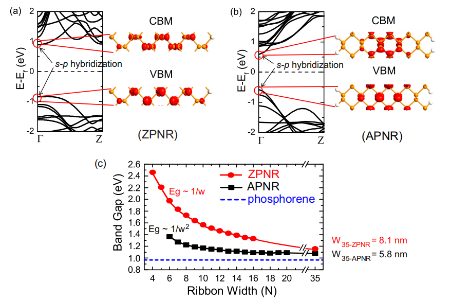
Figure 3. Band structures and partial charge densities of the CBM and VBM of the (a) 8-ZPNR and (b) 10-APNR. The distribution of charge densities shows both electrons and holes are distributed in the center of ribbons. (c) Variation of band gaps of APNRs (up to 5.8 nm) and ZPNRs (up to 8.1 nm) as a function of ribbon width N [5].
The band gap of phospholene is layer number dependent, which can change from 0.3 eV of the block to 1.5 eV in a single layer. This energy gap is distributed in the visible light range, which has good external field regulation performance, so that phospholene is not subject to a single band gap in practical application and has a better application prospect. Zhang et al. Try to graphene nanobape in different directions of the electric field, found that the perpendicular to the surface of the electric field does not affect the properties of electronic structure of black phosphorus nanobape, and join the transverse electric field can effectively adjust the nanoband gap, and with an increase in electric field, can realize the passivation of black phosphorus nanobape semiconductor characteristics to metal characteristics.
4. Comparison of graphene nanoribons with phosphorene nanoribbons in practical applications
High carrier mobility and good ON/OFF ratio is the key to measure the electrical performance of the material, and it is also an important index to judge whether the material can be applied in the field of tiny electronic components. Combined with the first two sections, phosphorene nanoribbons seem to be better than graphene nanoribbons in terms of the intrinsic band gap. However, phosphorene nanoribbons have high chemical reactivity and are easy to be oxidized for aging phenomenon. Considering the actual preparation and application, the effects of different preparation methods on the performance of nanoribbons are also different. In this section compares the performance of two different preparation methods and their products (mainly field effect transistors).
On the premise of considering opening the band gap, many preparation methods of graphene nanoribons have been produced. There are two mainstream methods: top-down and bottom-up. The former is not enough accuracy but the preparation is wide, while the latter is vice versa. The top-down method includes two-dimensional sheet etching, and open carbon nanotube; the bottom-up method includes organic synthesis, chemical vapor deposition, etc. In the study of top-down method, Hwang et al. used the CVD method to grow graphene on copper foil, and prepared graphene nanoribbons with a width of about 12 nm using HSQ as a mask, which opened the graphene band gap of about 0.1 eV [6]. At high source leakage bias field, current density exceeds 1000, room temperature current ION/IOFF≈10 and 4 K temperature ON/IOFF≈1×106. Sun et al. prepared graphene about 5 nm wide in oxygen plasma, increasing the ON/OFF ratio at room temperature to ION/IOFF≈47 [7]. Using nanowires as masks to obtain 8 nm width graphene nanobape field effect transistor [8], and the ION/IOFF≈160 at room temperature. In the study of bottom-up method, Bokor et al. obtained graphene nanoribbon with armchair-type boundary of N=9 and armchair-type boundary of N=13, and obtained the device with ION/IOFF≈105 at room temperature [9]. All in all, graphene nanoribbon field effect tubes with a width above 10 nm can achieve a better turn-off at low temperature. At room temperature, the switch ratio decreases significantly, ranging from about 10 to 160; some width below 10 nm can achieve very good off at room temperature, but it still needs improvement.
With the research in recent years, there have been many methods to prepare more suitable phosphorene nanoribbons. It can be roughly divided into phosphorene etching method and solution method, Feng et al. uses electron beam lithography method to prepare armchair and serrated phosphorene nanoribbons, width as low as 60 nm [10], Matt et al. through low temperature amino method of lithium ion embedded in black phosphorus crystal, the compound is dispersed in inert solution through mechanical stirring, to produce a single layer of phosphorene nanoribbons with a width of 4~50nm, an average length of about 690nm. Liu et al. disperse red phosphorus crystal powder in anhydrous ethanol, which can prepare oligolayer red phosphorus nanoribbons on a large scale, with a thickness of less than 20 nm, a width of about 120nm and a length up to several micron. However, the high chemical reactivity of phosphorene nanoribbons is still a problem. Wood et al. proposed the use of encapsulation technology to protect the active phosphorous layer, which is effective [11].
In general, both graphene nanoribbons and black phosphoene nanoribbons still have many problems to be solved from theory to practice. The earlier start of graphene nanoribbons provides a variety of solutions for the defects of graphene nanoribbons that need to open the band gap, While the study of black phosphorene nanoribbons is still being advanced, graphene nanoribbons are now more likely to be used in practice.
5. Conclusion
Through comparison, this study finds that the gap between the electrical performance of graphene and phosphorene nanoribbons is not large, but they have unique problems. The problem of opening the band gap of graphene nanoribbons has been solved well with the in-depth research in recent years. The on/off ratio in low temperature environment has been considerable, but how to maintain a high level of switching ratio at room temperature is still a problem. Phosphorene nanoribbons has natural advantages, providing a guarantee for their high level of electrical performance, but also troubled by active chemical properties, and the precision and large-scale popularization of its production process is also a problem to be solved. Both graphene nanoribbons and phosphorene nanoribbons have good application prospects and have high possibilities to replace traditional electronic components such as copper. However, given the current development speed of both, it will still take some time before the practical application.
References
[1]. Celis A, Nair M N, Taleb-Ibrahimi A, et al. 2016 Journal of Physics D: Applied Physics 49(14) 143001
[2]. Novoselov K S, Geim A K, Morozov S V, et al. 2004 Science 306(5696) 666-669
[3]. Son Y W, Cohen M L, Louie S G. 2006 Physical review letters 97(21) 216803
[4]. Peng X, Copple A, Wei Q. 2014 Journal of Applied Physics 116(14) 144301
[5]. Wu Q, Shen L, Yang M, et al. 2015 Physical Review B 92(3) 035436
[6]. Hwang W S, Tahy K, Li X, et al. 2012 Applied physics letters 100(20) 203107
[7]. Sun J, Iwasaki T, Muruganathan M, et al. 2015 Applied Physics Letters 106(3) 033509
[8]. Bai J, Duan X, Huang Y. 2009 Nano letters 9(5) 2083-2087
[9]. Llinas J P, Fairbrother A, Borin Barin G, et al. 2017 Nature communications 8(1) 633
[10]. Feng X, Huang X, Chen L, et al. 2018 Advanced Functional Materials 28(28) 1801524
[11]. Wood J D, Wells S A, Jariwala D, et al. 2014 Nano letters 14(12) 6964-6970
Cite this article
Chen,Z. (2024). Comparison of graphene nanoribbons and phosphorene nanoribbons in electrical performance applications. Applied and Computational Engineering,60,93-98.
Data availability
The datasets used and/or analyzed during the current study will be available from the authors upon reasonable request.
Disclaimer/Publisher's Note
The statements, opinions and data contained in all publications are solely those of the individual author(s) and contributor(s) and not of EWA Publishing and/or the editor(s). EWA Publishing and/or the editor(s) disclaim responsibility for any injury to people or property resulting from any ideas, methods, instructions or products referred to in the content.
About volume
Volume title: Proceedings of the 4th International Conference on Materials Chemistry and Environmental Engineering
© 2024 by the author(s). Licensee EWA Publishing, Oxford, UK. This article is an open access article distributed under the terms and
conditions of the Creative Commons Attribution (CC BY) license. Authors who
publish this series agree to the following terms:
1. Authors retain copyright and grant the series right of first publication with the work simultaneously licensed under a Creative Commons
Attribution License that allows others to share the work with an acknowledgment of the work's authorship and initial publication in this
series.
2. Authors are able to enter into separate, additional contractual arrangements for the non-exclusive distribution of the series's published
version of the work (e.g., post it to an institutional repository or publish it in a book), with an acknowledgment of its initial
publication in this series.
3. Authors are permitted and encouraged to post their work online (e.g., in institutional repositories or on their website) prior to and
during the submission process, as it can lead to productive exchanges, as well as earlier and greater citation of published work (See
Open access policy for details).
References
[1]. Celis A, Nair M N, Taleb-Ibrahimi A, et al. 2016 Journal of Physics D: Applied Physics 49(14) 143001
[2]. Novoselov K S, Geim A K, Morozov S V, et al. 2004 Science 306(5696) 666-669
[3]. Son Y W, Cohen M L, Louie S G. 2006 Physical review letters 97(21) 216803
[4]. Peng X, Copple A, Wei Q. 2014 Journal of Applied Physics 116(14) 144301
[5]. Wu Q, Shen L, Yang M, et al. 2015 Physical Review B 92(3) 035436
[6]. Hwang W S, Tahy K, Li X, et al. 2012 Applied physics letters 100(20) 203107
[7]. Sun J, Iwasaki T, Muruganathan M, et al. 2015 Applied Physics Letters 106(3) 033509
[8]. Bai J, Duan X, Huang Y. 2009 Nano letters 9(5) 2083-2087
[9]. Llinas J P, Fairbrother A, Borin Barin G, et al. 2017 Nature communications 8(1) 633
[10]. Feng X, Huang X, Chen L, et al. 2018 Advanced Functional Materials 28(28) 1801524
[11]. Wood J D, Wells S A, Jariwala D, et al. 2014 Nano letters 14(12) 6964-6970