


1. Introduction
In recent years, Ga2O3 semiconductor materials with excellent performance have entered the public field of vision, with high dielectric constant, breakdown voltage, and Baliga’s Figure of Merit [1-4], which is more advantageous than Si, SiC, GaN materials. In addition, single crystals can be grown using low-cost and low-loss technology [5-8], thus reducing production costs for mass production, which has strong practical application value.
Because the current research on Ga2O3 MOSFETs is relatively few and the preparation technology is immature, many studies use simulation software to simulate the performance of the components. By calculating the simulation process steps and simulating the electrical characteristics of the power device, Silvaco TCAD can roughly predict the experimental results and provide guidance for the actual experiments. This makes the experiment cost greatly reduced, and can speed up the experiment process, aslo avoiding the occurrence of large errors. At present, many scholars have used simulation methods to conduct a large number of studies on the electrical characteristics and reliability of Ga2O3 MOSFET. Man Hoi Wong et al. used Silvaco Atlas to simulate the electrical characteristics of Ga2O3 MOSFET at different temperatures to explore the influence of its self-heating effect on thermal resistance [9]. Inhwan Lee et al. proposed non-field plate (NFP) devices and field plate (FP) Ga2O3 MOSFET devices, obtained the static characteristics of the devices in Silvaco TCAD software, and conducted their switching performance in Silvaco mixed-mode with inductive load test circuits [10]. Junsung Park et al. used TCAD simulation to study the electrical performance of multi-gate vertical β-Ga2O3 MOSFETs and proposed a simulation setting based on β-Ga2O3 devices, and found that the ID- VGS simulation curve fitted well with the practice [11]. These studies have proved the accuracy and reliability of Silvaco TCAD.
This paper is divided into five parts: In the second part, it will explain how to use Silvaco TCAD to simulate according to the simulation idea, the simulation model and the simulation process sequence. In the third part, Ga2O3 MOSFET will be simulated to explore the effect of its structure on the electrical characteristics. In the fourth part, the research on the reliability of Ga2O3 MOSFET in recent years will be described. In the fifth part, the full text is summarized.
2. Simulation method
Before using Silvaco TCAD for simulation, it is necessary to obtain the specific structure of the simulation device and related data. Next, a variety of parameters are set, including material parameters such as electron affinity, band gap width, state density, saturation speed, etc. Model parameters, such as mobility, impact ionization parameters, etc. Numerical calculation methods, such as newton iteration method, gummel iteration method and block iteration method. After setting, print and tonyplot functions can be used to display the electrical characteristics of the device, as well as internal carrier concentration distribution and electric field distribution [13].
We chose the device model that used Silvaco Atlas to simulate wide-band gap Ga2O3 MOSFET for the first time in 2013 [12].
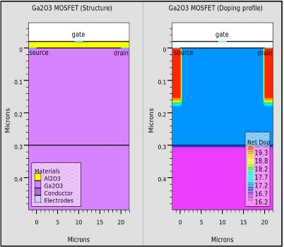
Figure 1. Device structure and doping [12]
The substrate is a semi-insulating single-crystal β-Ga2O3, above which there is a 300nm thickness N-type Ga2O3 channel layer with a dopant concentration of 7×1017 cm-3, about half of which can be considered activated. The source and drain contact regions were formed by multiple silicon implants with a deep box profile of 150 nm and a concentration of 5×1019 cm-3, of which 3×1019 cm-3 is activated. The distance between the source and drain box regions is 20 um, while forming a 20 nm thick Al2O3 gate dielectric film with a 2 um long Ti/Pt/Au metal gate at the top. According to the analysis, the effective mass of electrons is 0.28m0, the local conduction band density is NC=3.72×1018 cm-3, the electron affinity of β-Ga2O3 is 4.0 eV, and the work function of the gate is 5.23 eV [12].
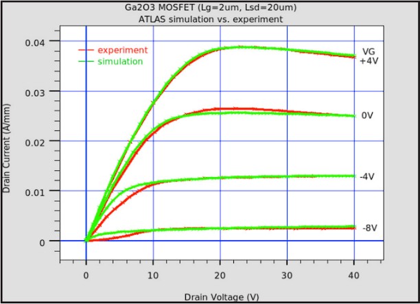
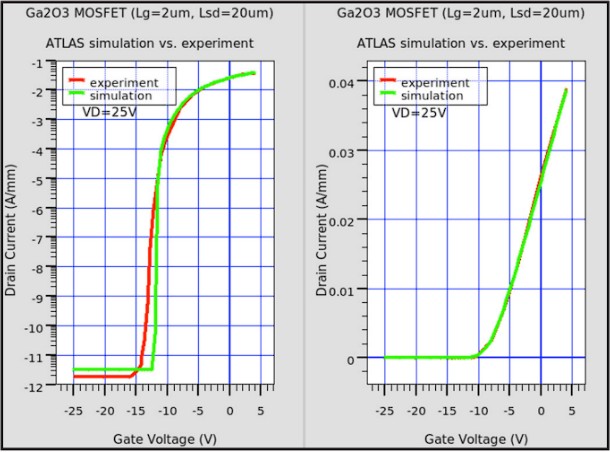
The simulated ID-VD curve and ID-VG curve are shown in Figure 2 and Figure 3. Figure 2 shows the relationship between ID and VD under different VGS, while Figure 3 shows the relationship between ID and VG. It can be seen that the simulation curve fits well with the experimental curve, which proves that the simulation calculation of Silvaco Atlas has high accuracy.
|
| |
Figure 2. Relationship between ID and VD. [12] | Figure 3. Relationship between ID and VG. [12] |
3. Simulation and analysis of electrical characteristics of Ga2O3 MOSFET
The electrical characteristics of Ga2O3 MOSFET can be affected by a variety of factors, such as the field plate, the environment, doping, fin shape, etc. This section will introduce the characteristics of its breakdown voltage and on-resistance.
Zeng Ke et al. proposed a new field plate design using composite dielectric, and used ALD deposited film in the high field region, which greatly improved the breakdown voltage of MOSFET power devices [14].
| Figure 4. Cross section of the improved Ga2O3 MOSFET structure [14]. |
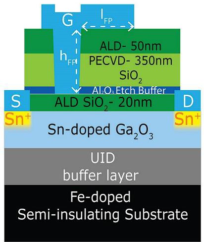
As shown in Figure 4, in order to avoid the breakdown outside the channel, a composite field plate is added on the top of the device, the upper part of which is composed of a higher density 50nm ALD SiO2 layer, the lower part is composed of 350nm PECVD SiO2 layer [14], and the lFP in the figure is optimized. In addition, a dielectric liquid Fluorinert (FC-770) is used instead of air, which has a dielectric constant 4 times that of air and can effectively prevent air breakdown.
|
| |
Figure 5. Breakdown voltage in different media. [14]. | Figure 6. Electric field simulation of Silvaco Atlas [14]. |
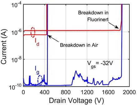
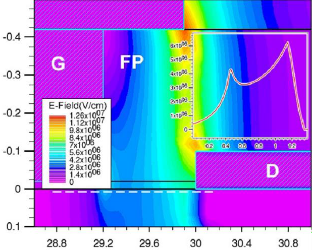
The actual breakdown voltage of the device was measured using a specific device. As shown in Figure 5, When dielectric liquid Fluorinert is used, the breakdown voltage is greatly increased relative to air, reaching an extremely high 1850V. In addition, the dielectric constant also correlates with the electric field strength in the device. Measurements on a device Lgd=0.8μm showed a breakdown voltage of 324V at a -32V gate bias under a fluorine noble gas, resulting in an average calculated electric field strength of 4.4±0.2MV/cm, higher than the 3.8MV/cm record reported in reference [15]. Meanwhile, in the electric field simulation of Silvaco Atlas (FIG. 6), the peak electric field intensity near the drain edge of the device is 6.1 MV/cm, which is higher than the actual value of 4.4 MV/cm. Although there is a certain error, the successful prediction of the rising trend of the electric field strength is of guiding significance to the experiment.
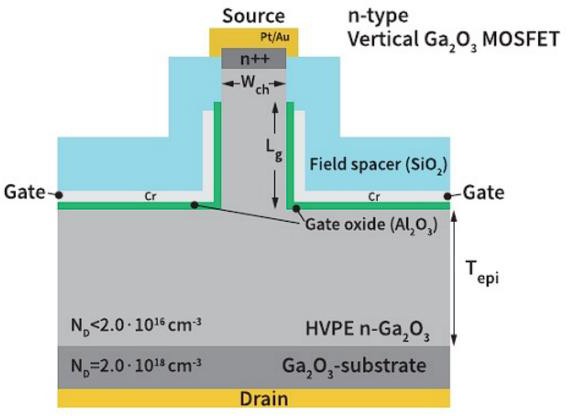
Junsung Park et al. found that the fin shape of a β-Ga2O3 vertical MOSFET has an effect on the on-resistance of the device, and used Silvaco TCAD to simulate the electrical performance. The structure of the proposed β-Ga2O3 vertical MOSFET is shown in Figure 7.
|
Figure 7. Structure of β-Ga2O3 vertical MOSFET [11]. |
The experiment made changes to the channel width (Wch) and fin height (Lg) of the fin structure, and measured the on-resistance of the device at different Wch and Lg, as shown in Figure 8(a). Considering the DIBL characteristics of the device, when Lg= 1.0 μm, Wch= 0.3μm, the overall performance of the device reaches the optimal value, and can achieve a very low DIBL (< 5 mV/V) while maintaining a low Ron per unit area.
|
| ||
| Figure 8. (a) Change of on-resistance under different Lg and different Wch. (b) Channel current simulation. (c) Drain current simulation [11]. | ||
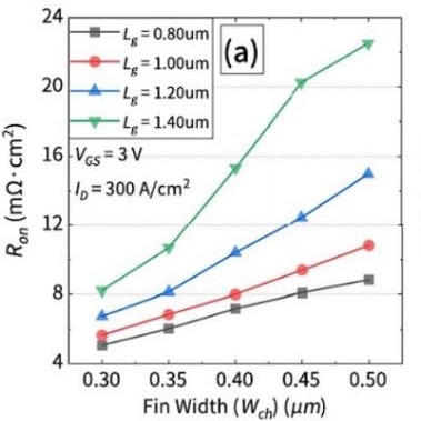

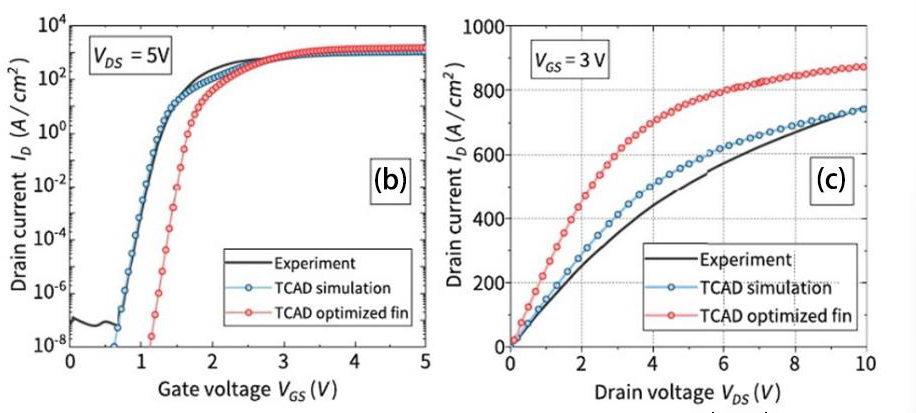
At the same time, TCAD simulation was carried out on the changes of channel current and drain current of the device. FIG. 8(b) shows that the TCAD simulation curve fits well with the experimental results, and the predicted threshold voltage (Vth) of the improved fin increases from 0.92V to 1.44V, indicating that its conductive ability has been improved. FIG. 8(c) simulates the ID-VDS curve, and finds that the maximum drain current is also increased, and the on-resistance at VDS=0V is reduced from 6.55 mΩ·cm2 to 4.78 mΩ·cm2. Silvaco TCAD accurately predicted the change in the on-resistance of the device.
4. Simulation and analysis of reliability of Ga2O3 MOSFET
Ga2O3 MOSFET also has some reliability problems, such as performance reduction caused by self-heating effect, switching loss caused by device switching process, etc. This chapter will show the application of Silvaco TCAD in reliability research.
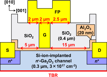
Due to the highly localized power dissipation and heat generation of MOSFET in the submicron region of the gate drain edge channel, as well as the self-heating effect caused by the low thermal conductivity of Ga2O3, Ga2O3 MOSFET power devices will degrade performance at high temperatures. Reference [9] shows a method of using TCAD to study the self-heating effect of MOSFET devices. The MOSFET device structure used in the study is shown in Figure 9.
|
Figure 9. Ga2O3 MOSFET device structure [9] |
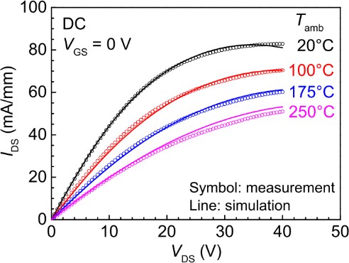
After parameter setting, the device was actually measured and Silvaco TCAD simulated. FIG. 10(a) shows the IDS-VDS curve at different temperatures with DC voltage. It can be found that the simulation curve fits well with the experimental results, which proves the reliability of TCAD.
|
| |
Figure 10. (a) IDS-VDS curve under DC [9] | (b) IDS-VDS curve under 5-μs pulse current [9] |
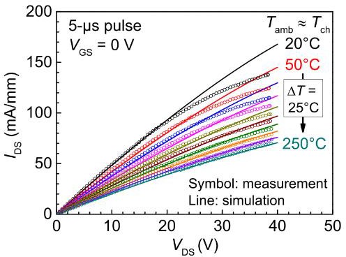
Next, the device is subjected to a 5-μs pulsed drain current and the IDS-VDS curve is measured and simulated (Figure 10b). At this time, it can be found that the experimental results fit well with the simulation results at low voltage, but the IDS of the experimental results is lower when the VDS simulation results is high, indicating that when VDS increases, the self-heating effect in the Ga2O3 channel becomes non-negligible and the thermal resistance of the device increases. This has also been verified in literature [16], where the saturation current of VLD transistors using SH (self-heating effect) model is significantly lower than that without SH model, indicating that the low thermal conductivity of Ga2O3 has a greater impact on device performance. These studies prove that the direct influence of the self-heating effect on the electrical characteristics of Ga2O3 MOSFET devices can be obtained through TCAD simulation.
Switching loss refers to the energy loss of a MOSFET during switching, which can affect its efficiency, temperature and reliability. Literature [10] found that the switching loss of the device can be reduced through field plate and width optimization.
Table 1. Switching loss of NFP and switching loss of FP under different TFPOX [10]
Drain current(Id) | 10A | 20A | 30A |
Eon-NFP (mJ) | 0.782 | 1.579 | 2.368 |
Eoff-NFP (mJ) | 0.963 | 1.886 | 2.795 |
Eon-FP (TFPOX = 0.5 μm) (mJ) | 0.324 | 0.587 | 0.892 |
Eoff-FP (TFPOX = 0.5 μm) (mJ) | 1.486 | 2.498 | 3.358 |
Eon-FP (TFPOX = 1.0 μm) (mJ) | 0.286 | 0.5215 | 0.802 |
Eoff-FP (TFPOX = 1.0 μm) (mJ) | 0.687 | 1.571 | 2.202 |
|
|
Figure 11. NFP and FP device structure [10] | |

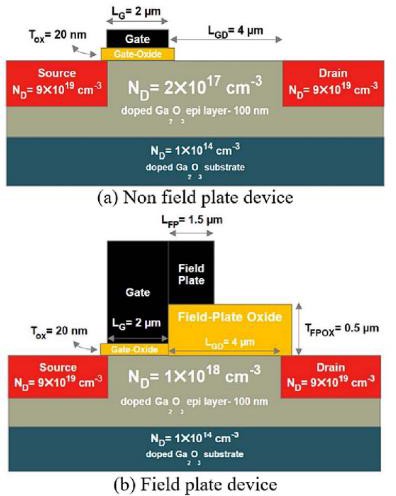
The device structure of NFP and FP is shown in FIG. 11. Band Gap energy is set at 4.8eV, Effective density of states in the condition band at 300k is at 4.45e-18 cm-3. Electron Affinity is set to 4.0eV and Electron Mobility is set to 118 cm2/V*s [10]. FP devices with TFPOX=1 μm can be found to have the lowest switching loss. However, compared with commercial SiC MOSFETs, although Ga2O3 devices have lower conduction loss, the switching loss is still high, so it is necessary to optimize the width of the devices. Silvaco TCAD is used to simulate the switching loss curve of the device width from 1.05e6μm to 2.0e6μm under different nominal power, as shown in FIG. 12.
|
|
| Figure 12. Power loss at different device widths [10] |
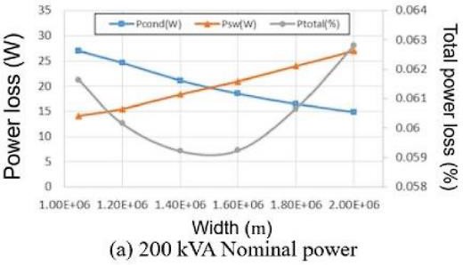
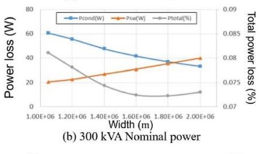
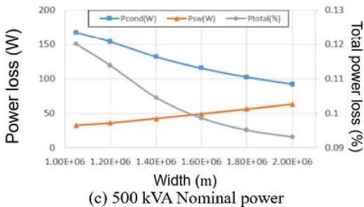
It can be concluded that the optimal device widths at 200, 300 and 500kVA are 1.4e6, 1.8e6 and 2.0e6 μm, respectively, which have the smallest power loss at these device widths.
5. Conclusion
In summary, under the background that Ga2O3 MOSFETs are difficult to prepare and few studies have been conducted, Silvaco TCAD simulation software can be used to explore the characteristics of power devices with low cost and high efficiency. In this paper, the simulation method of Silvaco TCAD is introduced, and it is applied to the study of the electrical characteristics and reliability of Ga2O3 MOSFET. It is found that the electric field strength of the power device designed by the new field board can predict the change of its breakdown voltage, and the simulation software successfully predicts the rising trend of the electric field strength. In addition, the channel width and fin height of the β-Ga2O3 vertical MOSFETs can be optimized by simulation to reduce the on-resistance of the devices. At the same time, it can also be applied to explore the reliability of self-heating effect and switching loss of the device. These studies help to improve the performance and durability of MOSFETs, such as reducing power consumption and heating. But in addition to these studies, the material parameters of Ga2O3, device model setting, process simulation research and other aspects of the exploration is still less. It is expected that the parameters and models used by Silvaco TCAD could be more abundant and accurate in the future, so as to simulate Ga2O3 MOSFETs more accurately, and be applied in more studies.
References
[1]. Von Wenckstern H. Group‐III sesquioxides: growth, physical properties and devices. Advanced Electronic Materials. 2017 Sep;3(9):1600350.
[2]. Orita M, Ohta H, Hirano M, Hosono H. Deep-ultraviolet transparent conductive β-Ga 2 O 3 thin films. Applied Physics Letters. 2000 Dec 18;77(25):4166-8.
[3]. Onuma T, Saito S, Sasaki K, Masui T, Yamaguchi T, Honda T, Higashiwaki M. Valence band ordering in β-Ga2O3 studied by polarized transmittance and reflectance spectroscopy. Japanese Journal of Applied Physics. 2015 Oct 14;54(11):112601.
[4]. Hudgins JL, Simin GS, Santi E, Khan MA. An assessment of wide bandgap semiconductors for power devices. IEEE Transactions on power electronics. 2003 May 13;18(3):907-14.
[5]. Víllora EG, Shimamura K, Yoshikawa Y, Aoki K, Ichinose N. Large-size β-Ga2O3 single crystals and wafers. Journal of Crystal Growth. 2004 Oct 1;270(3-4):420-6.
[6]. Ohira S, Yoshioka M, Sugawara T, Nakajima K, Shishido T. Fabrication of hexagonal GaN on the surface of β-Ga2O3 single crystal by nitridation with NH3. Thin Solid Films. 2006 Feb 1;496(1):53-7.
[7]. Kuramata A, Koshi K, Watanabe S, Yamaoka Y, Masui T, Yamakoshi S. High-quality β-Ga2O3 single crystals grown by edge-defined film-fed growth. Japanese Journal of Applied Physics. 2016 Nov 15;55(12):1202A2.
[8]. Tomm Y, Reiche P, Klimm D, Fukuda T. Czochralski grown Ga2O3 crystals. Journal of crystal growth. 2000 Dec 1;220(4):510-4.
[9]. Wong MH, Morikawa Y, Sasaki K, Kuramata A, Yamakoshi S, Higashiwaki M. Characterization of channel temperature in Ga2O3 metal-oxide-semiconductor field-effect transistors by electrical measurements and thermal modeling. Applied Physics Letters. 2016 Nov 7;109(19).
[10]. Lee I, Kumar A, Zeng K, Singisetti U, Yao X. Mixed-mode circuit simulation to characterize Ga 2O3 MOSFETs in different device structures. In2017 IEEE 5th Workshop on Wide Bandgap Power Devices and Applications (WiPDA) 2017 Oct 30 (pp. 185-189). IEEE.
[11]. Park J, Hong SM. Simulation study of enhancement mode multi-gate vertical gallium oxide MOSFETs. ECS Journal of Solid State Science and Technology. 2019 Mar 8;8(7):Q3116.
[12]. Silvaco A. Atlas simulation of a wide bandgap Ga 2 O 3 MOSFET. The Simulation Standard. 2013 Oct;23(4):7-9.
[13]. He M, Zeng F, Cheng WC, Wang Q, Yu H, Ang KW. Beta-Ga 2 O 3 MOSFET Device Optimization via TCAD. In2020 4th IEEE Electron Devices Technology & Manufacturing Conference (EDTM) 2020 Apr 6 (pp. 1-4). IEEE.
[14]. Zeng K, Vaidya A, Singisetti U. 1.85 kV breakdown voltage in lateral field-plated Ga2O3 MOSFETs. IEEE Electron Device Letters. 2018 Jul 23;39(9):1385-8.
[15]. Green AJ, Chabak KD, Heller ER, Fitch RC, Baldini M, Fiedler A, Irmscher K, Wagner G, Galazka Z, Tetlak SE, Crespo A. 3.8-MV/cm Breakdown Strength of MOVPE-Grown Sn-Doped β-Ga2O3 MOSFETs. IEEE Electron Device Letters. 2016 May 17;37(7):902-5.
[16]. Zhou X, Liu Q, Xu G, Zhou K, Xiang X, He Q, Hao W, Jian G, Zhao X, Long S. Realizing high-performance β-Ga₂O₃ MOSFET by using variation of lateral doping: a TCAD study. IEEE Transactions on Electron Devices. 2021 Feb 12;68(4):1501-6.
Cite this article
Rui,B. (2024). Electrical characteristics and reliability of gallium oxide devices study via TCAD simulation. Applied and Computational Engineering,65,138-146.
Data availability
The datasets used and/or analyzed during the current study will be available from the authors upon reasonable request.
Disclaimer/Publisher's Note
The statements, opinions and data contained in all publications are solely those of the individual author(s) and contributor(s) and not of EWA Publishing and/or the editor(s). EWA Publishing and/or the editor(s) disclaim responsibility for any injury to people or property resulting from any ideas, methods, instructions or products referred to in the content.
About volume
Volume title: Proceedings of Urban Intelligence: Machine Learning in Smart City Solutions - CONFSEML 2024
© 2024 by the author(s). Licensee EWA Publishing, Oxford, UK. This article is an open access article distributed under the terms and
conditions of the Creative Commons Attribution (CC BY) license. Authors who
publish this series agree to the following terms:
1. Authors retain copyright and grant the series right of first publication with the work simultaneously licensed under a Creative Commons
Attribution License that allows others to share the work with an acknowledgment of the work's authorship and initial publication in this
series.
2. Authors are able to enter into separate, additional contractual arrangements for the non-exclusive distribution of the series's published
version of the work (e.g., post it to an institutional repository or publish it in a book), with an acknowledgment of its initial
publication in this series.
3. Authors are permitted and encouraged to post their work online (e.g., in institutional repositories or on their website) prior to and
during the submission process, as it can lead to productive exchanges, as well as earlier and greater citation of published work (See
Open access policy for details).
References
[1]. Von Wenckstern H. Group‐III sesquioxides: growth, physical properties and devices. Advanced Electronic Materials. 2017 Sep;3(9):1600350.
[2]. Orita M, Ohta H, Hirano M, Hosono H. Deep-ultraviolet transparent conductive β-Ga 2 O 3 thin films. Applied Physics Letters. 2000 Dec 18;77(25):4166-8.
[3]. Onuma T, Saito S, Sasaki K, Masui T, Yamaguchi T, Honda T, Higashiwaki M. Valence band ordering in β-Ga2O3 studied by polarized transmittance and reflectance spectroscopy. Japanese Journal of Applied Physics. 2015 Oct 14;54(11):112601.
[4]. Hudgins JL, Simin GS, Santi E, Khan MA. An assessment of wide bandgap semiconductors for power devices. IEEE Transactions on power electronics. 2003 May 13;18(3):907-14.
[5]. Víllora EG, Shimamura K, Yoshikawa Y, Aoki K, Ichinose N. Large-size β-Ga2O3 single crystals and wafers. Journal of Crystal Growth. 2004 Oct 1;270(3-4):420-6.
[6]. Ohira S, Yoshioka M, Sugawara T, Nakajima K, Shishido T. Fabrication of hexagonal GaN on the surface of β-Ga2O3 single crystal by nitridation with NH3. Thin Solid Films. 2006 Feb 1;496(1):53-7.
[7]. Kuramata A, Koshi K, Watanabe S, Yamaoka Y, Masui T, Yamakoshi S. High-quality β-Ga2O3 single crystals grown by edge-defined film-fed growth. Japanese Journal of Applied Physics. 2016 Nov 15;55(12):1202A2.
[8]. Tomm Y, Reiche P, Klimm D, Fukuda T. Czochralski grown Ga2O3 crystals. Journal of crystal growth. 2000 Dec 1;220(4):510-4.
[9]. Wong MH, Morikawa Y, Sasaki K, Kuramata A, Yamakoshi S, Higashiwaki M. Characterization of channel temperature in Ga2O3 metal-oxide-semiconductor field-effect transistors by electrical measurements and thermal modeling. Applied Physics Letters. 2016 Nov 7;109(19).
[10]. Lee I, Kumar A, Zeng K, Singisetti U, Yao X. Mixed-mode circuit simulation to characterize Ga 2O3 MOSFETs in different device structures. In2017 IEEE 5th Workshop on Wide Bandgap Power Devices and Applications (WiPDA) 2017 Oct 30 (pp. 185-189). IEEE.
[11]. Park J, Hong SM. Simulation study of enhancement mode multi-gate vertical gallium oxide MOSFETs. ECS Journal of Solid State Science and Technology. 2019 Mar 8;8(7):Q3116.
[12]. Silvaco A. Atlas simulation of a wide bandgap Ga 2 O 3 MOSFET. The Simulation Standard. 2013 Oct;23(4):7-9.
[13]. He M, Zeng F, Cheng WC, Wang Q, Yu H, Ang KW. Beta-Ga 2 O 3 MOSFET Device Optimization via TCAD. In2020 4th IEEE Electron Devices Technology & Manufacturing Conference (EDTM) 2020 Apr 6 (pp. 1-4). IEEE.
[14]. Zeng K, Vaidya A, Singisetti U. 1.85 kV breakdown voltage in lateral field-plated Ga2O3 MOSFETs. IEEE Electron Device Letters. 2018 Jul 23;39(9):1385-8.
[15]. Green AJ, Chabak KD, Heller ER, Fitch RC, Baldini M, Fiedler A, Irmscher K, Wagner G, Galazka Z, Tetlak SE, Crespo A. 3.8-MV/cm Breakdown Strength of MOVPE-Grown Sn-Doped β-Ga2O3 MOSFETs. IEEE Electron Device Letters. 2016 May 17;37(7):902-5.
[16]. Zhou X, Liu Q, Xu G, Zhou K, Xiang X, He Q, Hao W, Jian G, Zhao X, Long S. Realizing high-performance β-Ga₂O₃ MOSFET by using variation of lateral doping: a TCAD study. IEEE Transactions on Electron Devices. 2021 Feb 12;68(4):1501-6.